
Space engineering
Photovoltaic assemblies and components
Foreword
This Standard is one of the series of ECSS Standards intended to be applied together for the management, engineering and product assurance in space projects and applications. ECSS is a cooperative effort of the European Space Agency, national space agencies and European industry associations for the purpose of developing and maintaining common standards. Requirements in this Standard are defined in terms of what shall be accomplished, rather than in terms of how to organize and perform the necessary work. This allows existing organizational structures and methods to be applied where they are effective, and for the structures and methods to evolve as necessary without rewriting the standards.
This Standard has been prepared by the ECSS-E-ST-20-08C Rev.1 Working Group, reviewed by the ECSS Executive Secretariat and approved by the ECSS Technical Authority.
Disclaimer
ECSS does not provide any warranty whatsoever, whether expressed, implied, or statutory, including, but not limited to, any warranty of merchantability or fitness for a particular purpose or any warranty that the contents of the item are error-free. In no respect shall ECSS incur any liability for any damages, including, but not limited to, direct, indirect, special, or consequential damages arising out of, resulting from, or in any way connected to the use of this Standard, whether or not based upon warranty, business agreement, tort, or otherwise; whether or not injury was sustained by persons or property or otherwise; and whether or not loss was sustained from, or arose out of, the results of, the item, or any services that may be provided by ECSS.
Published by: ESA Requirements and Standards Division
ESTEC, ,
2200 AG Noordwijk
The
Copyright: 2012 © by the European Space Agency for the members of ECSS
Change log
|
ECSS-E-20-08A
|
First issue
|
|
ECSS-E-20-08B
|
Never issued
|
|
ECSS-E-ST-20-08C
|
Second issue
|
|
ECSS-E-ST-20-08C Rev.1
|
Second issue Revision 1
|
Introduction
The qualification, procurement, storage and delivery of space solar arrays are defined in the dedicated solar array specification, where requirements for the solar array electrical layout, structure and mechanism are specified.
This Standard outlines the requirements for the qualification, procurement, storage and delivery of the main assemblies and components of the space solar array electrical layout: photovoltaic assemblies, solar cell assemblies, bare solar cells, coverglass and protection diodes. This Standard does not outline the requirements for the qualification, procurement, storage and delivery of the solar array subsystem, comprising the solar panels, structural parts and mechanisms.
The general requirements are covered in the main part of this Standard (clauses 5 to 11). Annex A to Annex E specify the contents of the source control drawing of photovoltaic and solar cell assemblies, bare solar cells coverglasses and protection diodes and include the inspection data, physical and electrical characteristics, other ratings and acceptance and qualification specific requirements, which can be different for each space project.
This Standard is divided into five specific subjects, each one corresponding to each assembly or component:
Clause 5 defines requirements for photovoltaic assemblies,
Clause 6for solar cell assemblies,
Clause 7 for bare solar cells,
Clause 8for coverglasses,
Clause 9 for protection diodes.
Two additional clauses are dedicated to Sun simulators and calibration procedures (clause 10 and capacitance measurement methods (clause 11).
Scope
This Standard specifies the general requirements for the qualification, procurement, storage and delivery of photovoltaic assemblies, solar cell assemblies, bare solar cells, coverglasses and protection diodes suitable for space applications.
This standard does not cover the particular qualification requirements for a specific mission.
This Standard primarily applies to qualification approval for photovoltaic assemblies, solar cell assemblies, bare solar cells, coverglasses and protection diodes, and to the procurement of these items.
This standard is limited to crystaline Silicon and single and multi-junction GaAs solar cells with a thickness of more than 50 m and does not include thin film solar cell technologies and poly-crystaline solar cells.
This Standard does not cover the concentration technology, and especially the requirements related to the optical components of a concentrator (e.g. reflector and lens) and their verification (e.g. collimated light source).
This Standard does not apply to qualification of the solar array subsystem, solar panels, structure and solar array mechanisms.
This standard may be tailored for the specific characteristic and constrains of a space project in conformance with ECSS-S-ST-00.
Normative references
The following normative documents contain provisions which, through reference in this text, constitute provisions of this ECSS Standard. For dated references, subsequent amendments to, or revision of any of these publications do not apply, However, parties to agreements based on this ECSS Standard are encouraged to investigate the possibility of applying the more recent editions of the normative documents indicated below. For undated references, the latest edition of the publication referred to applies.
|
ECSS-S-ST-00-01
|
ECSS system – Glossary of terms
|
|
ECSS-Q-ST-60
|
Space product assurance — Electrical, electronic and electromechanical (EEE) components
|
|
ECSS-Q-ST-70-06
|
Space product assurance – Particle and UV radiation testing for space materials
|
|
ECSS-Q-ST-70-09
|
Space product assurance – Measurements of thermo-optical properties of thermal control materials
|
|
ISO 15387:2005
|
Space Systems – Single junction space solar cells – Measurement and calibration procedures
|
|
ISO 14644-1:1999
|
Cleanrooms and associated controlled environments – Part 1: Classification of air cleanliness
|
|
MIL-E-12397B
|
Eraser, rubber pumice for testing coated optical elements
|
|
IEC 60749-26:2006
|
Semiconductor devices – Mechanical and climatic test methods - Part 26: Electrostatic discharge (ESD) sensitivity testing – Human body model (HBM)
|
|
ASTM D1193-99
|
Standard specification for reagent water
|
|
ESCC 23800 Issue 1
|
Electrostatic Discharge Sensitivity Test Method
|
|
ESCC 24900 Issue 2
|
Minimum Requirements for Controlling Environmental Contamination of Components
|
|
DIN 53289
|
Testing of adhesives for metals; floating roller peel test
|
Terms, definitions and abbreviated terms
Terms from other standards
For the purpose of this Standard, the terms and definitions from ECSSSST0001 apply, in particular for the following terms:
qualification
verification
Terms specific to the present standard
General
blistering
forming of multiple small air bubbles inside the perimeter of a finish layer
bubbles
gaseous inclusion in the cell, coverglass or coverglass adhesive
chip
local absence of material along the edges and corners of a complete component and which extend through the thickness of the component
crack
fissure in the component with no separated portion from the remainder
Cracks can propagate from the edge of the material (edge cracks) or terminate at both ends within the material (surface cracks).
delamination
physical separation between two material layers, which are joined in design
discolouration
local variation of solar cell anti–reflection coating colour due to the influence of the structure orientation of the cell layer immediately below or the variation of the anti–reflection coating layer thickness
dig
cavities in the surface of a component caused by impact with a pointed object or by crushing a material into the surface
inclusion
volume contained within the component that is devoid of the substrate material
in–process testing
tests performed during the manufacturing of a component or assembly in order to identify, in advance, defects or low performances
nick
local absence of material on the surface of a complete component which does not extend through the thickness of the component
peeling
forming of a delamination of a finish layer at the edge of the finished area. A blister at the edge of the surface
procurement lot
set of shipment lots of solar cells assemblies, bare solar cells and coverglasses, manufactured with the same processes and materials, with identical manufacturing lines, that fill the same purchase order
scratch
linear marking of the component that represents a volume devoid of the substrate material emanating from a single face of the component and not penetrating through the whole thickness of the substrate at any point
shipment lot
solar cell assemblies, bare solar cells and coverglasses manufactured with the same processes and materials with identical manufacturing lines delivered to the customer as a part of a purchase order
spatter
small bits of solid coating material imbedded on or in the coating or substrate
voids
absence of deposited materials
Examples are absence of cell contact material or anti–reflection coating.
Photovoltaic assemblies
photovoltaic assembly
power generating network comprising the interconnected solar cell assemblies (strings and sections), the shunt and blocking diodes, the busbars and wiring collection panels, the string, section and panel wiring, the wing transfer harness, connectors, bleed resistors and thermistors
qualification coupon
non–flight representative test sample of flight panels, built with flight processes and containing representative materials and components to be used in the manufacture of flight panels, formerly also called DVT coupon
slicing
procedure to evenly distribute the total number of thermal cycles over temperature domains which are compatible with the temperature excursion on an orbit level rather than on the overall mission temperature envelope
Normally used for LEO missions.
Solar cell assemblies
cladding
application of a thin layer of material fully covering the surface, For instance silver cladding of an interconnector
deformed interconnector
interconnector whose initial conformed shape is modified
interconnected cell
solar cell with interconnector without coverglass
solar cell assembly
solar cell together with interconnector, coverglass and, if used, by–pass diode
tearing interconnector
interconnector physically separated from the cell due to a failure of the welding or soldering joint
Bare solar cells
bare solar cell
photovoltaic component capable to delivering electrical power when illuminated with light
component bare solar cell
specially manufactured solar cell, with only one active junction and the same spectral response as one sub cell of a multi–junction solar cell
contact vacuum evaporation batch
bare solar cells manufactured in the same contact vacuum evaporation run
drops
excess of metallization material on the solar cell contacts
remaining Factor
ratio of an electrical performance parameter at EOL to its value at BOL
E.g. maximum power of a solar cell.
solar cell anti–reflection coating
single or multi–layer coating which reduces the reflection coefficient of the incident solar radiation
uncoated area
area of the solar cell where the bare solar cell is exposed and is devoid of coatings
worm shaped bulge
protuberance of contact material shaped in linear irregular paths or single dots where the contact material is locally delaminated from the immediate lower layer
Coverglasses
coating
dielectric or conductive material applied to the glass substrate by vacuum deposition
Coatings applied to the external face of the coverglass is termed the “front surface coating”. Coatings applied to the internal face of the glass substrate to be bonded to the solar cell is termed the “rear surface coating”. Commonly used coatings include:
- single–layer anti–reflection coating,
- multi–layer anti–reflection coating,
- ultraviolet reflector,
- infrared reflector, and
- conductive coating.
conductive coating
transparent coating used to prevent the exposed surface from charging and consequently protecting the solar cell from the effect of electrostatic discharge
The coverglass usually comprises a suitable glass substrate and one or more of a combination of the coatings given in the note in clause 3.2.5.1.
coverglass
glass substrate and coatings applied to its surfaces
coverglass coating lot
collection of glass substrates subjected to the same coating run or runs (for coverglasses which have more than one coating)
infrared reflector
multi–layer dielectric coating which has a high reflectance coefficient in the infrared portion of the solar spectrum
The infrared reflector is used to reflect light that is not usefully converted to electrical energy by the solar cell thus reducing the operating temperature and increasing the conversion efficiency of the SCA.
mark
See stain
multi–layer anti–reflection coating
multiple layer coating which has the effect of increasing the transmission coefficient of the coverglass
single layer anti–reflection coating
simplest form of coating comprising a single layer of low index dielectric material which minimizes the reflection coefficient of the incident solar radiation thus increasing the transmission coefficient of the coverglass
The single layer of low index dielectrical material is usually done of MgF2.
stain
area which under inspection conditions can clearly be defined as not being optically homogeneous with the bulk material, and that cannot be categorized as an inclusion, scratch, crack, chip, dig, void or coating delamination
The term “mark” can be used as a synonymous.
ultraviolet reflector
multi–layer dielectric coating which has a high reflectance coefficient in the UV portion of the solar spectrum
The ultraviolet reflector is used to protect the underlying adhesive and to reflect light that is not usefully converted to electrical energy by the solar cell thus reducing the operating temperature of the solar cell and increasing the conversion efficiency of the SCA.
uncoated area
area of the coverglass where the bare coverglass substrate is exposed and is devoid of coatings
Verification processes
accelerated testing
test in which the life time requirement is verified in an accelerated way by intensifying one parameter of the environment or load.
The following are examples of accelerated tests:
- UV test done with increased sun intensity in the UV part of the spectrum,
- Electron and proton radiation tests with life time fluences in a limited period of time,
- humidity tests done at higher temperature and humidity,
- bake-out done at higher temperature,
- performance parameter degradation at higher temperature,
- thermal cycling with higher/lower cool-down and heat-up rates and without nominal operating dwell time in between.
acceptance test
test to determine that a system, subsystem, component or functional part is capable of meeting performance requirements prescribed in purchase specifications or other documents specifying what constitutes the adequate performance capability for the item and to demonstrate the item is free from manufacturing defects
In this document acceptance is associated with specified requirements which have a defined acceptance safety factor with respect to requirements corresponding with the actual loads and environments
delta qualification
qualification performed on an equipment which has undergone minor design modifications or has been qualified to operate in environments less severe than those specified
proto flight test
test requirements which have a defined qualification safety factor with respect to requirements corresponding with the actual loads and environments, but with limited test durations
qualification by similarity
process to demonstrate the ability to fulfil specified requirements by comparing a new design specification with a similar proven design specification
Abbreviated terms
For the purpose of this standard, the abbreviated terms of ECSS-S-ST-00-01 and the following apply:
|
Abbreviation
|
Meaning
|
|
ADP
|
acceptance data package
|
|
AOCS
|
attitude and orbit control system
|
|
AM0
|
air mass 0 (zero)
|
|
APTC
|
ambient pressure thermal cycling
|
|
AR
|
anti-reflection
|
|
ARC
|
anti-reflection coating
|
|
ATOX
|
atomic oxygen
|
|
BOL
|
beginning-of-life
|
|
BSC
|
bare solar cell
|
|
BSR
|
back surface reflector
|
|
CIC
|
connector integrated cell
|
|
CIDL
|
configuration item data list
|
|
CVCM
|
collected volatile condensable material
|
|
CVG
|
coverglass
|
|
DCR
|
documentation change request
|
|
DJF
|
design justification file
|
|
DRD
|
document requirements definition
|
|
DRB
|
delivery review board
|
|
DVG
|
direct voltage gradient
|
|
DVT
|
design verification test
|
|
EMC
|
electromagnetic compatibility
|
|
EOL
|
end-of-life
|
|
ESD
|
electrostatic discharge
|
|
FIT
|
failure in time
|
|
FMECA
|
failure modes, effects and criticality analysis
|
|
GaAs
|
gallium arsenide
|
|
GEO
|
geostationary orbit
|
|
IC
|
interconnected cell
|
|
Imp
|
maximum power current
|
|
Iop
|
current at operational voltage
|
|
IRR
|
infrared reflector
|
|
Isc
|
short-circuit current
|
|
IVG
|
inverted voltage gradient
|
|
LEO
|
low Earth orbit
|
|
LVDT
|
linear voltage displacement transducer
|
|
MLAR
|
multi-layer anti-reflection coating
|
|
NCR
|
nonconformance report
|
|
NRB
|
nonconformance review board
|
|
OSTC
|
on station thermal cycling
|
|
PAD
|
part approval document
|
|
PCDU
|
power control and distribution unit
|
|
PID
|
process identification document
|
|
Pmax
|
maximum power
|
|
PMCF
|
product manufacturing and control file
|
|
PMP
|
parts, materials and processes
|
|
PTH
|
power transfer harness
|
|
PVA
|
photovoltaic assemblies
|
|
r.m.s.
|
root mean square
|
|
RAMS
|
reliability, availability, maintainability and safety
|
|
RDC
|
relative damage coefficients
|
|
RML
|
recovered mass loss
|
|
S.C.
|
solar constant
|
|
S.C. (AM0)
|
solar constant at air mass 0
|
|
SCA
|
solar cell assembly
|
|
SCD
|
source control drawing
|
|
SLAR
|
single layer anti-reflection coating
|
|
SWS
|
secondary working standard
|
|
TAT
|
type approval test
|
|
D
|
to be defined
|
|
S
|
to be specified
|
|
TML
|
total mass loss
|
|
UVR
|
ultraviolet reflector
|
|
Vmp
|
maximum power voltage
|
|
Voc
|
open-circuit voltage
|
|
Vop
|
operational voltage
|
|
Vtest
|
test voltage
|
|
WRC
|
World Radiation Centre in Davos
|
General
Overview
Objective and organization
The objectives of this Standard are:
To define the rules for the flow of technical requirements from a project solar array specification down to component level in order to guarantee that lower level components and sub-assemblies are qualified according to specifications.
To define the set of requirements from component level up to photovoltaic assemblies (PVA) to enable a generic qualification for each level of assembly for about 90 % of the solar array applications within a certain range; for example, deployable solar arrays for GEO or LEO.
This clause describes the organization of the requirements and how they are applied.
The philosophy behind this Standard is two fold in that respect that:
Qualification of a specific level of assembly is based on the use of qualified components and sub-assemblies at lower levels. The specification hierarchy that photovoltaic assemblies and their components form part of is illustrated in Figure 41.
OR
Qualification of components for a specific application can be achieved at a sub-assembly level at which the qualification is unequivocally demonstrated. This means that certain types of qualification tests do not need to be duplicated at different level of assembly in case of a unique application of a dedicated design
This Standard defines the requirements for qualification at each level from components up to and including PVA on coupons. Coupons are built according to PVA design requirements with the objective of demonstrating that the design and manufacturing processes are ready for use on solar panels of a flight application.
For many parameters in this standard the value to be specified as requirement is dependent on the mission concerning duration and environmental conditions or the implemented solar array design. These parameter values are derived from the higher level subsystem specification and reflected in a dedicated document. In this standard the source control drawing has been selected generically on every level of assembly as an example of a document to reflect the specific requirements. So the source control drawing or equivalent set of documentation is the reference list for physical characteristics, performance requirements and environmental conditions.
Full qualification for an application is not only achieved after successful qualification of the PVA and its components on coupon level. Robustness against some environments can only be demonstrated in the final solar array configuration, that may comprise amongst others full size panel on-station thermal cycling and sine vibration, acoustic noise, and wing deployment testing at subsystem or spacecraft level.
 Figure 41: Specification hierarchy
Interfaces with other areas
In the specification hierarchy (Figure 41) only the components and assembly levels that are usually dedicated to solar arrays are shown. At every integration step, additional materials and components, not mentioned in the specification hierarchy, are used such as:
adhesives,
solder,
interconnectors and busbars,
diodes,
resistors,
thermistors,
connectors, and
wires.
Requirements for these materials and components can be found in their procurement specifications, and in EEE component specifications, which are reviewed as part of the qualification process. For EEE component specifications, see the ECSS-Q-ST-60 series of standards. For Materials Parts and processes specifications, see the ECSS-Q-ST-70.
The qualification of the use of these items is a pre-requisite for the qualification of the assembly they are part of (for example, coverglass adhesive at the SCA level and busbars at the qualification coupon level).
Non-PVA related solar array design, power subsystem interface and mission specific related topics such as grounding, electromagnetic compatibility, magnetic moment, spacecraft related geometrical loss factors and end-of-life performance prediction related topics, including loss factors, are not addressed in this Standard.
Specific design measures to support the solar array in order to satisfy the requirements of this Standard, such as grounding spots and blocking diodes, are however, taken into account.
Specific environmental conditions which can be a limitation in the qualification for general use, are not addressed in this Standard as these aspects are usually the subject of a project dedicated qualification (for example, the chemical contents in local ambient air).
Physical properties
The following physical properties of the components and materials shall be measured:
- coefficient of thermal expansion
- heat conductivity
- specific heat
- Young’s modulus and Poisson’s ratio
- Flex strength
The objective is to establish the boundaries for the qualification test program over the full range of application by means of analysis.
The data specified in requirement 4.2a shall be determined during the development phase of a new component and need not be repeated during the qualification program.
Test and storage
Test environment
The atmospheric conditions during all inspection, test operations and storage shall be as follows:
- Pressure: (1 013,25 33) hPa.
- Temperature: (23 5) C.
- Average relative humidity: 40 % - 60 %.
A pressure of (1 013,25 33) hPa is equivalent to (760 25) mmHg.
The room cleanliness level should be airborne particle count: Class 8 ISO 14644-1.
Every deviation from requirements 4.3.1a and 4.3.1b during tests shall be recorded in the data documentation package (DDP).
- 1 For DDP complete contents, refer to Annex G.
- 2 Semiconductor devices (i.e. planar diodes) can short-circuit if no special precautions are taken during long storage periods under certain atmospheric conditions. This is because chlorine content, in combination with illumination, can produce metal contact migrations on these semiconductor devices.
Test tolerances and accuracies
The accuracy of the instruments and test equipment used to control or measure test parameters shall be one order of magnitude higher than the tolerance on the variable to be measured.
Examples of where this cannot be achieved include measurements of electrical performance and temperatures.
All instrumentation used for qualification and acceptance tests shall:
- be calibrated, and
- be within the specified calibration period at the time of test.
Instrumentation whose calibration period runs out during the planned test time shall not be used.
The maximum test temperature tolerances for thermal testing shall be as given in Table 41.
The accuracy of mass measurements shall be better than 1 % or 0,01 g, whichever is higher.
The test condition tolerances shall be applied to the nominal test values specified.
The accuracy of the electrical performance test on PVA level shall be better than or equal to the calibration loss factor used in the power analysis.
TableTable 41: Test tolerances on temperature
|
Temperature range (C)
|
tolerance (C)
|
|
around - 175
|
-10 / +0
|
|
around - 100
|
-10 / +0
|
|
around + 90
|
-0 / +10
|
|
Around +130
|
-0 / +10
|
Margins
The margins to be applied to qualification test conditions shall be as defined in the solar array specification.
Critical materials
The critical interface information shall be part of the PMP list.
For PMP, see ECSS-Q-ST-70 Annex B.
Silver cladding shall be annealed and contain a minimum of 99,9 % pure silver.
Pure tin, cadmium and zinc shall not be present in finished space-qualified solar panels.
Pure tin refers to a tin alloy with less than three atomic percent of an alloying metal, e.g., lead. Pure cadmium and zinc is defined as these metals used or applied in a non-mixed metal or unalloyed state.
Solar panels containing Beryllium Oxide shall be clearly identified with the designation BeO.
Photovoltaic assemblies
Overview
Description
The photovoltaic assembly (PVA) comprises the electrical parts to satisfy the requirements of the solar array specification.
This Clause applies to solar arrays using a planar design without concentration and based on crystalline solar cells.
In case of concentration, this Clause applies to the PVA without the optics, provided that the electrical performance tests are adapted to the light incidence and intensity imposed by the optics.
Usually, a PVA consists of parallel connected strings. A string is the smallest operational component at the PVA level. A string consists of a series interconnected solar cells connected to the spacecraft bus. These strings are supported by a solar array panel substrate or frame.
The parts comprising a PVA usually include:
interconnected SCAs,
bleed resistors,
wiring,
panel connectors,
diodes (blocking and shunt),
thermal sensors,
telemetry indicator wiring, and
grounding.
Purpose and objective
In this Clause the design limits, including margins, and the responsibilities for PVA manufacturing are defined and include the:
design requirements (refer to clause 5.3);
mechanical and electrical interface;
manufacturing requirements for PVA (refer to clause 5.4);
qualification requirements for PVA (refer to clause 5.5.1);
acceptance requirements for PVA (refer to clause 5.5.2).
The values specified for the SCA level are provided by the solar cell assembly supplier and confirmed during the SCA qualification tests (refer to clause 6.4).
In order to design and verify a solar array, data for the following parameters and characteristics at the SCA level or lower are used:
characteristics of the SCA (Voc, Isc, Vmp and Imp);
spectral response;
reference calibration standard;
relative damage coefficient and electron-proton equivalence;
temperature coefficients as a function of radiation fluences;
reverse characteristics versus temperature;
UV and Sun spectrum characteristics (reflectivity);
capacitance versus temperature;
optical properties (hemispherical emissivity, and solar absorptance, and cover gain or loss);
behaviour with regard to specific mission environments:
ATOX sensitivity,
thruster erosion sensitivity,
micro-meteoroids and debris sensitivity;
loss factors for interconnecting the cells into a string.
Conditions and method of test
The conditions and methods of testing shall conform to the photovoltaic assembly source control drawing (SCD-PVA).
The PVA specification consists of two parts, the generic specification (this Standard) and the SCD. For the preparation of the SCD-PVA, refer to Annex A.
The SCD-PVA shall be prepared by the supplier, in conformance with Annex A, and provided to the customer for reviewing and agreement.
Any deviation from in-process, acceptance and qualification test shall be justified.
Deviations from this Standard applicable to the SCD-PVA shall:
- be agreed between the customer and the supplier;
- include alternative requirements equivalent to those of this Standard;
- not affect the reliability and performances of the photovoltaic assemblies;
- be only those specified in requirement 5.2c.
Photovoltaic assembly design
Overview
The objective of this standard at the PVA level is to specify the requirements for the detail design, performance, qualification, manufacture and acceptance testing of coupons equipped with the PVA. The inputs to these requirements are the solar array specification, which is prepared following the requirements of the mission specification, the ground test programme and the spacecraft design. In this clause the steps which influence specific design characteristics of the PVA have been listed. Requirements which merely determine the sizes of the PVA have not been taken into account, like intensity related loss factors and reliability requirements.
Parameters related to parts, materials and processes (PMP)
Outgassing
Flight hardware shall be constructed from space qualified materials having the following properties:
- A recovered mass loss (RML) of 1 % or less.
See ECSS-Q-ST-70-02.
- A collected volatile condensable material (CVCM) of 0,1 % or less when heated in a vacuum to 125 C and collected at 25 C. The PMP list shall include the RML and CVCM values for all materials used.
The mission specification can specify an absolute limit to the total mass loss and volatile condensable material of the solar array sub-system. The fulfilment of this system requirement can be verified either by analysis using the total amount of the applied materials, the individual material RML and CVCM data, outgassing field of view and temperature distribution, or by test of the representative subsystem and measurement of the outgassing product.
Toxicity
Any material used in the construction of the PVA that is dangerous to the health of the personnel shall be identified.
Preventive handling measures shall be taken in conformance with a standard approved by the customer.
Flammability
Any flammable materials used in the construction of the PVA shall be identified.
Corrosion
The supplier and customer shall agree on the measures to be taken to prevent corrosion during storage or in normal operational service.
Standard atmospheric conditions may be assumed for general applications in the spacecraft, over a period of time that is agreed between the supplier and customer.
To avoid electrolytic corrosion, a process, approved by the customer, shall be used.
Magnetism
Permanent magnetic materials shall be avoided when specified by the mission.
Non-magnetic materials should be used.
Erosion
PVA materials shall be capable of tolerating a defined erosion level resulting from spacecraft operation without degradation in the nominal performance of the PVA, in conformance with the PVA specification.
Example: thruster plumes.
Atomic oxygen (ATOX)
PVA materials shall be capable of tolerating a defined level of degradation resulting from an ATOX environment, without degradation in the nominal performance of the PVA, in conformance with the solar array specification.
The ATOX resistivity shall be determined by the individual resistivities of the used materials and components in their configuration.
Parameters related to design
Cell integration
The solar cells shall be structured such that the PVA is capable of withstanding all phases of ground handling, transportation, qualification testing and acceptance testing, launch and orbit operations as to conform to the mission requirements.
The capability for replacement of cracked, broken or damaged SCAs shall be included in the design.
Repair method shall be feasible in horizontal and vertical panel positions.
Stringing
If blocking diodes are applied in the design at the panel level, the positive end of the strings shall be connected to the panel connector by a blocking diode.
To enable performance measurement at the lowest level of assembly at the coupon level, strings shall be measured individually.
Potential parallel connections shall not prevent performance measurement specified in requirement 5.3.3.2b.
If the dimensions of the coupon enables the accommodation, the full flight string length shall be represented on the qualification coupon.
Coupon layout shall be as defined in a overall assembly drawing as part of the SCD-PVA.
Cell interspacing
The cell interspacing shall be compatible, as a minimum, with the following mission requirements:
- thermal expansion and contraction within the mission temperature extremes specified in the solar array specification;
- panel geometry;
- ESD requirements.
Sectioning
Sections shall not be included at the coupon level.
To test the technique of interconnecting strings, the negative ends of individual strings may be connected in a way that is representative for flight panels.
Reverse bias protection
The solar cells that are potentially subject to reverse bias shall be protected by shunt diodes unless the solar cells are insensitive to the effects of reverse bias.
Types of reverse bias include:
- AOCS failure shadowing,
- self shadowing, and
- power management (including maximum power point tracker when direct energy transfer function is acting at BOL).
Insulation
The following items shall be electrically insulated from each other:
- Any solar cell circuits to substrate (the grounding reference of the coupon).
- Solar cell circuits to solar cell circuits (if not connected at the negative ends).
- Thermal sensor to the solar cell circuits and to the substrate (the grounding reference of the coupon).
- Conductive coverglass grounding network, if used, to solar cell circuits.
Derating
For the derating requirements of components, see ECSS-Q-ST-30-11.
Redundancy
For redundancy requirements, see ECSS-Q-ST-30.
For failure modes requirements, see ECSS-Q-ST-30-02.
Fault tolerance
A FMECA shall be performed for the design of the solar array.
The design consequences shall be implemented on the qualification coupon, including:
- the photovoltaic assembly from solar cell strings to the connector, and
- redundant bleed resistors and, if any, redundant PVA assemblies or components.
- 1 Examples: Solar cell strings, blocking diodes, temperature sensors.
- 2 For FMECA, see ECSS-Q-ST-30-02.
No single fault shall result in the following: - The loss of integrity of the redundant parts indicated in requirement 5.3.3.9b.2.
- The propagation of the fault causing permanent damage or loss of use of the units connected to the PVA.
Examples: solar array regulator unit, solar array drive mechanism.
No failure shall be propagated from one solar array wiring group to another.
Fatigue resistance
The effects of fatigue shall be verified by analysis or test.
The design of the PVA shall include the result of the verification specified in requirement 5.3.3.10a.
Adherence to substrate
Measurement
The adherence of SCAs to the substrate shall be measured using representative process samples.
Property
The SCAs shall stay attached to the panel and conform to all requirements during the test campaign and all the phases of the mission.
The adherence shall be such that the SCAs integrated on the substrate can be repaired, removed and replaced.
Adhesive uniformity
The thickness boundaries, including manufacturing and repair tolerances, shall be defined by means of analysis or test.
The boundary requirements on minimum and maximum thickness, in conformance with requirement 5.3.3.12a, shall be guaranteed by a controlled application process demonstrated on separate samples.
The thermal conductance towards the panel substrate shall be such that the specified solar cell and protection diode temperature can be maintained.
Electrostatic discharge (ESD)
The solar array design shall be such that it can survive the charging environment and operating conditions defined by the mission.
Requirement 5.3.3.13a shall be either demonstrated by analysis or by testing.
During and after launch, the spacecraft is surrounded by a low density plasma of high energy electrons and protons. On insulated surfaces of the spacecraft, the electrons build up a charge which discharges when breakdown of the insulating materials is reached.
Electromagnetic compatibility (EMC)
The PVA shall be designed to meet the specific EMC requirements stated in the SCD-PVA.
Repairability
The capability of repairing, removing and replacing items down to component level shall be provided.
For example, for single SCAs, diodes, thermal sensors, wires and connectors.
PVA manufacturing
Process validation
The manufacturing and integration processes shall be validated for all the project specific design configurations and to meet the engineering design requirements.
Defect acceptability
The acceptability of defects at the PVA level shall be:
- agreed with the customer;
- defined in a production control document;
- validated by qualification testing.
In-process testing
Overview
The in-process tests are performed during the manufacturing of the PVA to detect deviations and defects as early as possible. This clause 5.4.3 lists the test to be performed during the manufacturing of the PVA.
Mass measurement
To determine the add-on mass of the SCA laydown process, the mass of the substrate shall be measured before and after the substrate is equipped with the SCA’s and be in conformance with SCD-PVA.
Wet insulation test
A wet insulation test shall be performed by the supplier to prove the integrity of the bare coupon insulation layer, as follows:
- Verify continuity between the conductive layer under the insulation to the test connection point.
- For the wet insulation test, use ethyl, isopropyl alcohol, or otherwise an equivalent fluid agreed with the customer, as contact fluid during the measurements.
- Apply a voltage which corresponds to the breakthrough value for short term exposure of the applied insulation material (Espec V/m) times the minimum guaranteed thickness.
For example, for Espec= 20 V/m and a (50 10) m insulation layer, a test voltage of 800 V applies.
The acceptance criteria shall be an insulation larger than 100 M.
In case of a failure, the coupon insulator layer shall be repaired.
Adherence to substrate
The adherence of the SCAs to the substrate, shall be performed in parallel to panel laydown.
The adherence to substrate shall be verified by means of one of the following two methods:
- Method 1
- Bond 3 SCAs following identical process to a representative PVA substrate of the following dimensions: 200 x 130 mm.
- After 1 week at room temperature, perform a pull test, with a pull force equal or larger than 1 N/cm2.
- Method 2
- In case no solar cell assemblies and substrate are available, bond together 2 Kapton foils of the same material as used in representative PVA and with dimensions of 250 mm x 150 mm.
- After 1 week at room temperature, perform a peel test of the foil according to DIN 53289.
- Use a peel force equal or larger than 1,8 N/cm.
- Ensure that the separation takes place within the adhesive for an area larger than 50 %.
Visual inspection
A visual inspection shall be made after stringing.
This is to determine, as early as possible, defects in the rear sides of solar cells and, when feasible, the front sides.
The visual inspection procedure and criteria shall be agreed with the customer and be described in the SCD-PVA.
Continuity check
The continuity of all strings shall be checked after stringing, in order to detect defects not detected during the visual inspection.
Continuity of harness, wires and diodes shall be checked, and measured after final assembly.
The maximum values of resistance shall be given in the SCD-PVA.
Identification and traceability
Components other than SCAs, bare cells and coverglasses shall be identified in conformance with the traceability requirements of Class 1 components, and PAD DRD of ECSS-Q-ST-60.
For requirements on the identification and traceability of parts and materials, see clauses 6.1.4, 7.1.3 and 8.3.3 for SCAs, bare cells and coverglass, respectively.
Recording
Before start manufacturing, all processes and process variables related to PVA manufacturing that have impact on the performance of the process, shall be identified by the supplier.
The processes variables specified in requirement 5.4.5a shall be recorded during manufacturing.
PVA tests
Qualification tests
Purpose
Qualification tests are performed to check and qualify the design requirements.
Process
Qualification tests shall be preceded by the acceptance tests as listed in clause 5.5.2, in order to be representative of the life of flight hardware.
All results of the qualification test shall be reported in a qualification test report.
Qualification margins shall not exceed component and material specifications unless agreed between supplier and customer.
The following environmental test shall be performed for qualification of PVAs as applied on solar panels:
- Fatigue thermal cycling test on the qualification coupon.
- Humidity test performed on dedicated test sample if not tested on SCA level.
- ESD test on a dedicated ESD coupon, if specified by the solar array requirement specification.
- Erosion of materials, due to thruster plume if specified by the solar array requirement specification.
The tests to be performed for each qualification are listed in Table 51 and described in clauses 5.5.2 and 5.5.3.
In cases where the same coupon is used for the fatigue thermal cycling test and the humidity test, in conformance with requirement 5.5.1.2d the humidity test sequence shall precede the fatigue thermal cycling test sequence.
Except in conformance with requirement 5.5.1.2e, each type of test shall be performed on a dedicated qualification coupon built specifically for the test.
The qualification coupon need not be the same size as the flight panels, but shall contain a representative number of components to enable reliable verification of flight panel processes and materials.
The processes used to build the qualification coupon shall be documented in a parts, materials and process (PMP) list to ensure that the flight panels are built with identical processes, materials and configurations.
Each qualification coupon shall be flight representative as far as allowed by the dimensions of the qualification coupon
Facilities shall be available to safely store the qualification hardware (included failed samples) for a minimum of 6 years (equivalent to five years in storage and one year in orbit).
TableTable 51: Qualification test plan for PVA
|
Check
|
Fatigue thermal cycling
|
Humidity test
|
ESD test
|
|
Full visual inspection (5.5.3.2)
|
1, 6, 9, 14
|
1, 5
|
1, 4
|
|
Electrical health check and performance (5.5.3.3 and 5.5.3.4)
|
2, 7, 10, 15
|
2, 6
|
2, 5
|
|
Capacitance (5.5.3.5)
|
3, (11), 16
|
|
|
|
X-ray photo (5.5.3.9)
|
4, (12), 17
|
|
|
|
Reflectance (5.5.3.8)
|
|
3, 7
|
|
|
Vacuum thermal cycling (5.5.3.11)
|
5, 13
|
|
|
|
Substrate integrity (5.5.3.10)
|
18
|
|
|
|
Fatigue thermal cycling (5.5.1.3)
|
8
|
|
|
|
Humidity (5.5.1.4)
|
|
4
|
|
|
ESD test (5.5.1.5)
|
|
|
3
|
|
NOTE: The numbers in each column indicate the sequence in which the checks are performed for each test.
| |||
Fatigue thermal cycling test
Purpose
The purpose of the thermal cycling test is to demonstrate the life fatigue compatibility of all components and processes in an assembly.
General
The PVA manufacturer shall demonstrate that lack of continuity is avoided at any time during cycles defined in requirement 5.5.1.3.4g, both on the solar cell and on the protection shunt diode circuits.
The test conditions, specifically the thermal gradients through the test sample thickness, shall be representative of the distribution predicted in space so that the components are not over-stressed or under-stressed beyond specified limits.
The temperature extremes of the thermal cycling shall be extended or a dedicated structural test shall be performed in cases where analysis demonstrates that the structural loading results in a greater stress than the thermal cycling.
For example, acoustic and noise can produce greater stress than thermal cycling in certain missions.
Qualification coupon
The qualification coupon shall be defined by means of a representative drawing, document or matrix in the SCD-PVA.
The representation of the critical areas of the solar array on the qualification coupon shall be agreed with the customer.
For example, the substrate represents a worst-case stress part of the flight panels.
The qualification coupon shall be manufactured using the same qualified materials and processes as the flight panel, and any deviation shall be identified by the PVA supplier.
The qualification coupon shall contain only one PVA technology.
The number of (non-cell) components shall correspond to the number in a flight configuration of the unit they belong to, but with a minimum of two.
For example, it can be one blocking diode per string, one shunt diodes per shunt interval, and two bleed resistors per panel, but in accordance with this requirement, in all these cases the minimum number is two.
If space is available, additional components may be included to be tested as separate items.
For every type of solar cell configuration (N-end tab, P-end tab or middle cell) one piece shall be repaired on the coupon after the acceptance test (only visual inspection and electrical health check), unless configurations are identical, in which case at least two cells shall be repaired.
The production of the qualification coupons shall be representative of the full processing of the flight hardware.
At least 3 thermocouples on the front side and 3 on the rearside of each qualification coupon shall be placed for temperature monitoring.
The qualification coupon subjected to the fatigue thermal cycling test need not follow the acceptance test sequence.
Dedicated electrical test points shall be included in the electrical design of the qualification coupon such that the capacitance of single strings can be measured.
Test
The number of cycles and temperature deltas may be determined using one of the following criteria:
- The number of cycles is four times the number of cycles that occur during the mission with 0 C temperature delta (at both upper and lower design temperature limit).
- The number of cycles is equal to 1,5 times the number of cycles occurring during the mission with a temperature delta of 10 C at extremes (both upper and lower qualification temperature limit).
If qualification margin temperature exceeds the brittle point of main elements of the PVA, the option to be used in conformance with requirement 5.5.1.3.4a shall be agreed with the customer.
For a GEO mission, the following cycling profiles shall be used: - Define GEO transfer orbit cycles in conformance with the mission profile.
- all on station representing fatigue cycles are identical”. For a LEO mission, the following cycling profiles shall be used:
- A temperature profile which envelopes the variation of temperature extremes during the mission.
- The total profile, divided into a number of equally shaped sub-profiles, where the number of sub-profiles are:
- equal to the number of years of the mission, and
- with extreme cycle temperatures derived from the slicing of the temperature profile of the whole mission.
The number of cycles and temperature limits of requirements 5.5.1.3.4a and 5.5.1.3.4b shall be stated in the SCD-PVA.
Monitoring of the insulation between the solar cell circuit and the substrate shall:
- be performed in conformance with clause 5.5.3.3.3, and
- take place during the cycles with the maximum temperature limits and for a minimum of two cycles at each test interval. Monitoring of the continuity of the solar cell circuits shall:
- be performed in conformance with clause 5.5.3.3.2,
- take place during cycles for the complete activity,
- be performed on a regular, at least daily basis for a number of cycles, such that:
- during 10 % of these cycles of the cell circuit, and
- during 90 % of these cycles on the protection diode network shall be monitored.
- be performed by measuring both cell circuit continuity, at the beginning and at the end of the cycles in conformance to the relevant percentage specified in requirement 5.5.1.3.4g.3. Insulation and continuity shall not be measured simultaneously.
Pass-fail criteria
On completion the test, the following conditions shall be met:
- there is electrical continuity (no open circuit), and
- the power output of the test coupon and the insulation is within the limits stated in the SCD-PVA.
Humidity
Purpose
The purpose of the humidity test is to demonstrate the endurance of assembled PVA components in a real-life environment against standard environmental conditions using accelerated tests.
General
If there are requirements on specific environmental conditions, they shall be stated in the SCD-PVA.
For example, chemical vapour requirements.
Test Sample
The test sample shall be manufactured using the same qualified materials and processes as the flight panels.
The production of the test sample shall be representative of the full processing of the flight hardware.
Test
The test sample shall be placed in a chamber at ambient pressure.
The chamber temperature shall then be increased to 60 C minimum.
Relative humidity shall be higher than 90 %.
The duration of the test shall be 30 days.
In the case of solar cells with aluminium content window layers, the HT test shall be extended to simulate on-ground expected duration and humidity and temperature conditions.
High-purity water in conformance with ASTM D1193-99, Type I, shall be used.
Water condensation on the surface of the test sample shall be prevented.
If there are requirements on specific environmental conditions, they shall be stated in the SCD-SCA.
For example, requirements on chemical vapour conditions.
Pass-fail criteria
On completion the test, the following conditions shall be met:
- there is electrical continuity (no open circuit), and
- the power output of the test coupon and the insulation is within the limits stated in the SCD-PVA for the specified temperatures.
Electrostatic discharge (ESD) test
Purpose
The purpose of the ESD test is to demonstrate that the use of adequate design rules reduces the risk of ESD. This is done by demonstrating that ESD primary discharge does not lead to a self-sustained secondary arc, which can lead to loss of permanent power or insulation in the solar array.
The tests are performed on solar array coupons using instrumentation specially designed for that purpose.
Typical rules and a test procedure are described in ECSS-E-ST-20-06.
Pass-fail criteria
No sustained arc shall occur.
Testing shall demonstrate that the observed primary arcs do not produce any type of damage to the solar array or to the cells.
Erosion of materials
The test sequence, test definitions and requirements for the tests for erosion of material shall be agreed between the supplier and the customer and stated in the SCD-PVA.
EMC
The test sequence, test definitions and requirements related to the EMC of the PVA shall be agreed between the supplier and the customer and given in the SCD-PVA.
Acceptance tests for qualification coupons
Purpose
The acceptance tests are performed to check the workmanship of the supplier.
Applicability
Acceptance test are applicable to completed and qualified hardware, except if the acceptance tests are part of the qualification process.
Deliverables
The deliverable documentation shall be agreed with the customer.
The acceptance is dependent on this test and the documentation delivered.
Process
All acceptance tests shall be in conformance with clause 5.2.
All results of the acceptance test shall be reported in the data documentation package (DDP).
For the DDP, see clause 5.7 and Annex G.
The standard sequence of acceptance tests for PVA shall be as presented in Table 52.
The bake-out test shall be performed as part of the coupon acceptance test sequence only in the cases where the bake-out is included in the manufacturing process or in the acceptance test of the flight panels.
TableTable 52: Acceptance test plan
|
Sequence number
|
Test
|
|
Add-on mass (5.5.3.1)
|
0
|
|
Full visual inspection (5.5.3.2)
|
1, 6, 10
|
|
Electrical health check (5.5.3.3)
|
2, 7, 11
|
|
Capacitance (5.5.3.5)
|
3, 13
|
|
Electrical performance (5.5.3.4)
|
4, 8,12
|
|
Bake-out (5.5.3.6)
|
5
|
|
Thermal cycling (5.5.3.7)
|
9
|
|
NOTE: See 5.5.2.4d
| |
Definition of tests and checks
Add-on mass measurement
The mass of the panel shall be measured after the coupon is equipped with the PVA parts and the harness, and the add-on mass deduced.
The add-on mass of both the PVA and the harness shall be in conformance with the value given the SCD-PVA.
Full visual inspection
Purpose
The full VI is performed to detect imperfections in the complete hardware.
Process
A full visual inspection shall be performed against the inspection requirements stated in clauses 5.5.3.2.4 to 5.5.3.2.21, as follows:
- Visually examine each component for workmanship, identification and finish.
- Examine the deliverable items for conformance to general assembly drawings, with respect to critical dimensional parameters.
The inspection methods to be used include:
- electroluminescence
- infrared inspection;
- inspection with the naked eye;
- inspection using microscopes;
- any equivalent methods.
Training records of the personnel performing the visual inspection shall be made available to the customer under request.
General criteria
The PVA supplier shall define the inspection criteria for the PVA components, to be agreed by the customer, and included in the SCD-PVA.
Visual inspection of dimensions, stay-out zones, and stand-offs
The dimensions shall conform to the qualification coupon assembly drawing.
Cells and components shall not enter the stay-out zones indicated on the qualification coupon assembly drawing.
The stand-off distance of cells and components shall conform to the qualification coupon assembly drawing.
Visual inspection of the substrate
Substrates shall be inspected for any damage due to coupon assembly, handling and testing.
The insulator material shall show no evidence of delamination.
The insulator material is usually kapton.
The integrity of the substrate shall not deviate from the coupon assembly drawing.
Visual inspection of the coverglass
All the coverglass shall be inspected for defects in conformance with requirements 5.5.3.2.6b to 5.5.3.2.6e.
No more than 5 % of the total number of coverglasses shall exhibit any of the following defects on the coupon, due to assembly, handling and acceptance:
- For 100 % covered cells, or cells where the unprotected solar cell surface is covered with the coverglass adhesive up to a maximum of 5 % of the cell area, chips and nicks in the coverglass with the characteristics specified in clause 6.4.3.1.4.
- Cracks on the coverglass, except if they meet the following conditions:
- no visible separation (in conformance with clause 6.4.3.1.4);
- no more than three per cover;
- meeting cracks if they are separated by more than 2 mm at the non-meeting end.
Any defect in conformance with requirement 5.5.3.2.6b, raised after acceptance shall be reported and traced throughout the qualification sequence.
Covers with dirty and contaminated surfaces shall be cleaned.
Coverglasses with any of the following defects shall be rejected at the end of acceptance:
- Coverglasses installed upside down as indicated by improper location of the coating orientation mark in conformance with clause 8.3.3.
- Coverglass which is not flush with or overhanging all four cell edges.
- Coverglasses with dirty and contaminated surface if they cannot be cleaned.
- Loose coverglasses.
- Corner chip exceeding the limits specified in requirement 5.5.3.2.6b.1.
- Edge chips exceeding the limits specified in clause 6.4.3.1.4.
- Coverglasses with intersecting cracks exceeding the limits specified clause 6.4.3.1.4.
Visual inspection of the coverglass adhesive
After coverglass or solar cell repair, there shall be no delamination or discoloration in the adhesive, except in the area opposite rear welds, where discoloration may be present.
After coverglass or solar cell repair, adhesive voids along the cover edge shall not exceed 0,6 mm in depth.
After coverglass or solar cell repair,, the maximum total projected area of additional bubbles shall not exceed 0,2 % of cell area, discounting:
- bubbles less than 0,02 mm2 in the projected area, and
- bubbles, discolorations and voids located at less than 2 mm from the interconnector edges.
Visual inspection of the solar cells
No more than 2 % of the total quantity of solar cells or one cell, whichever is larger, per coupon shall exhibit any of the following defects:
- More than the number of cracks per cell specified in the SCD-PVA.
- Cracks crossing more than the number of different gridlines specified in the SCD-PVA.
- Corner chips and edge chips greater than those specified in clause 6.4.3.1.4.
Any imperfections listed in requirements 5.5.3.2.8a.1 to 5.5.3.2.8a.3, raised after acceptance shall be reported and traced throughout the qualification sequence.
Solar cells with any of the following defects shall be rejected at the end of acceptance: - Cracks crossing more gridlines than defined in requirement 5.5.3.2.8a.2.
Multiple crossing of the same gridline can be present.
- More cracks than defined in requirement 5.5.3.2.8a.1 on a single cell.
- Cracks between the cell edges parallel to the gridlines and the outermost edges of the interconnectors.
- Corner chip exceeding the limits specified in clause 6.4.3.1.4.
- Edge chips exceeding the limits specified in clause 6.4.3.1.4.
Visual inspection of the solar cell bypass diodes
Cracks in the body of the diode, causing separation of the material, shall not be present.
Tarnishing of the diode body or attachment serpentines may be present.
Visual inspection of the interconnectors
No more than 2 % of the total number of interconnectors and no more than one interconnector per cell shall exhibit any of the following defects at the end of acceptance testing:
- Deformation.
- Solder or adhesive blocking, bridging, plugging or otherwise impeding the flexure of the stress relief loop.
- Foreign matter or contamination on the interconnector or within the interconnector weld or solder joint or within the stress relief loop.
Any imperfections listed in requirements 5.5.3.2.10a.1 to 5.5.3.2.10a.3, raised after acceptance shall be reported and traced throughout the qualification sequence.
None of the interconnectors shall exhibit lifting tears, breaks or cracks.
Interconnectors may be tarnished.
Visual inspection of the bus bars
None of the bus bars shall exhibit any of the following defects at the end of acceptance testing:
- Solder or adhesive blocking, bridging, plugging or otherwise impede the flexure of stress relief loops between solar cell strings.
- Foreign matter, or contamination on the interconnector, within the interconnector weld or solder joint, or within the stress relief loop.
- Tears, breaks or cracks.
Any defect listed in requirements 5.5.3.2.11a.1 to 5.5.3.2.11a.3, raised after acceptance shall be reported and traced throughout the qualification sequence.
Tarnishing may be present on the end terminations.
Visual inspection of the wiring
None of the wiring shall exhibit any of the following defects at the end of acceptance testing:
- Sharp bends, sharp twists, sharp buckles or creases in the wire.
- Delamination or looseness of the wire attachment.
- Chafing or abrasion of the wire insulation.
- Cracks, breaks or nicks in the wire insulation or conductor.
- Exposed shields on shielded wires. Any defects listed in requirements 5.5.3.2.12a.1 to 5.5.3.2.12a.5, raised after acceptance shall be reported and traced throughout the qualification sequence.
Visual inspection of the soldering
Soldering of wires at string terminations and terminals shall be in conformance with a standard agreed with the customer
For soldering, see for instance ECSS-Q-ST-70-08.
Visual inspection of the welding
Welding of wires at string terminations and terminals shall be in conformance with the SCD-PVA.
Visual inspection of the crimping
Crimping of wires shall be in conformance with a standard agreed with the customer.
For crimping, see for instance ECSS-Q-ST-70-26.
Visual inspection of the attachment materials
Attachments based on bonding techniques shall be fully cured and not exhibit any tackiness.
Visual inspection of the feed-throughs
Feed-throughs shall be firmly bonded.
Feed-throughs shall conform to the locations specified on the top assembly drawing.
Visual inspection of the marking
All identification markings specified by the customer shall be firmly adhered to the locations identified on the assembly drawing.
Identification markings shall be clearly legible.
Visual inspection of the hardware
Terminal board locations shall conform to the qualification coupon assembly drawing.
Stand-off of all components shall conform to the qualification coupon assembly drawing.
For mounted components (temperature sensor, resistors and diodes), the following shall be performed:
- Verify the status of the following items:
- fixation on the substrate;
- body aspect and absence of cracks;
- connections;
- shrinkage tube.
- Ensure that conformal coating of the components,:
- consist of a uniform layer of the specified adhesive, and
- encapsulate the components.
For the connectors, the status of the following items shall be verified:
- fixing on the substrate;
- absence of cracks;
- connections;
- shrinkage tube.
Visual inspection of the bonding integrity
100 % of the solar cells shall be inspected for bond integrity.
Any loose cells shall not be used unless an engineering disposition, specifying that it can be used, is issued.
Visual inspection of the cleanliness
When visually examined with the unaided eye, the coupon shall appear clean.
There shall be no loose material on the coupon.
Electrical health check
Purpose
All tests specified in this clause are part of the electrical health check. The purpose of the electrical health check together with the electrical performance measurement is to detect faults in the electrical functions of the electrically active parts of the PVA.
Electrical continuity check
All electrical circuits of the PVA shall be checked to ensure electrical continuity, and the test conditions shall be stated in the SCD-PVA.
Insulation resistance
An insulation test shall be performed at the voltage stated in the SCD-PVA to measure the insulation between the following:
- the structure ground or substrate (+) and the solar cell circuits (-) including soldering and wiring;
- adjacent solar cell strings if not parallel connected;
- the thermal sensor (+) and the substrate (-);
- the thermal sensor (+) and cell strings (-);
- the cover glass network (-) to cell strings (+) if the coverglass network is grounded;
- the cover glass network (+) to cell strings (-) if the coverglass network is grounded. The insulation shall be in conformance with that stated in the SCD-PVA.
Grounding resistance test
All resistance at grounding spots shall be measured.
The grounding resistance shall be the value stated in the SCD-PVA.
Bleed resistor test
The resistance of the bleed resistor shall be measured.
The resistance shall be the value stated in the SCD-PVA.
Blocking diode test
The reverse current of the blocking diode shall be measured of at a voltage equal to the predicted maximum Voc during the mission.
The reverse current measured shall be negligible with respect to the string current (usually less than 5 mA).
The forward voltage drop of the blocking diode shall be measured with the string at maximum Isc current.
Test conditions and requirements shall be stated in the SCD-PVA.
Shunt diode test
When all the cells are protected by shunt diodes, the forward voltage of shunt diodes shall be measured by reverse mode measurement of the interconnected string at the maximum operating current and the measured voltage shall be equal 1 % to the sum of the individual diode forward voltages at the maximum current.
When all the cells are protected by shunt diodes, the supplier shall provide the test method and precautions to be taken.
When all the cells are protected by shunt diodes, during the test, the temperature increase of the shunt diode shall be uniform and shall not exceed the value stated in the SCD-PVA.
If the measured voltage is outside the sum of the individual diode forward voltages at the maximum current 1 %, techniques such as thermographic photo recordings may be used to locate the failed shunt diodes.
Thermal sensor test
The thermal sensor resistance shall be measured at room temperature.
The thermal sensor resistance shall be the value stated in the SCD PVA.
Resistance measurement
The resistance of the harness shall be measured at the interface connector by measuring the redundant coupon wiring in series (i.e. positive end to positive end and negative end to negative end).
Test conditions and requirements shall be described in the SCD-PVA.
Electrical performance measurement
Purpose
The power output is measured in order to be able to detect any degradation before and after testing.
Process
The electrical power performance at the string level shall be measured at a reference temperature of 25 C at the interface connector.
The performance measurement shall be made under 1 S.C. (AM0).
The characteristics of the Sun simulator are given in clause 10.
The results shall be in conformance with those stated in the SCD-PVA.
The inaccuracies in current, voltage and power shall be specified in the SCD-PVA and include:
- spectral mismatch;
- uniformity of the test area;
- dynamic electrical effects of the test item
Example: capacitance.
- inaccuracies of the temperature sensors.
Calibration shall be done with an agreed primary standard reference and secondary working standard (SWS) in conformance with clause 10.
Pre-test and post-test measurements shall be made with the same test setup.
Capacitance test
Purpose
The purpose of the test is to measure the capacitance of the PVA by measuring the string capacitance in order to characterise the electrical dynamical behaviour of the PVA in interaction with the power regulator. Different types of power regulator require different measurement techniques. The methods described in clause 5.5.3.5.2 are applicable only to PVA interacting with a sequential switching shunt regulator.
Process
One of the following methods shall be followed for capacitance measurement:
- frequency domain single junction solar cell capacitance measurement as described in clause 11.1,
No method available for multi-junction measurement at the time being.
- Time domain capacitance measurement as described in clause 11.2.
The method for measuring the capacitance shall be stated in the SCDPVA.
The capacitance shall be measured at room temperature and averaged operational temperature.
The measurement at averaged operational temperature can be replaced by measurement of the SCA capacitance at operational temperature.
Bake-out
Measures to prevent outgassing, to be taken before exposure to vacuum conditions, shall be agreed with the customer.
If a vacuum bake-out at the panel level is specified in the solar array specification, a vacuum bake-out shall be performed on the PVA before thermal cycling at coupon level.
Temperature and test conditions shall be defined in SCD-PVA.
Thermal cycling acceptance test
Purpose
The thermal cycle acceptance tests assess the reliability of the PVA under stress and verify the workmanship of the supplier. In this way infant mortality stresses are identified and these parts can be replaced.
General
Thermal vacuum cycling should be used.
If gaseous cycling tests are used, the supplier shall demonstrate the equivalence of the test method.
The temperature extremes of the thermal cycling shall be extended or a dedicated structural test shall be performed in cases where analysis demonstrates that the structural loading results in a greater stress than the thermal cycling.
Process
The panels shall be exposed to the number of thermal cycles for acceptance as stated in the SCD-PVA.
The number of cycles specified in requirement 5.5.3.7.3a shall be between 4 and 10.
The temperature profile shall be the worst-case nominal temperature profile with a 5 C margin.
During thermal cycling, the electrical insulation shall be measured.
During thermal cycling, the continuity shall be measured at least during the last cycle.
Continuity and insulation shall not be measured simultaneously.
Acceptance criteria shall be:
- A maximum increment of IOP, and a minimum isolation, as stated in the SCD-PVA.
- The existence of electrical continuity (no open circuit).
- At the end of the test, less than a 2 % increase in cracked cells or one cracked cell, whichever is higher, not cumulative with the results of the bake-out test and which can have an impact on the electrical performance of the string.
Reflectance
The reflectance of the solar cell surface shall be measured before and after the humidity test to determine the possible degradation of the coverglass coatings.
The reflectance shall be measured over a range from 280 nm to 2 500 nm.
The reflectance shall not change during testing more than as stated in the SCD-PVA.
X-Ray
X-ray photographs shall be taken of all busbars, wire collection strips and diode boards on the qualification coupons.
The acceptance criteria shall be stated in the SCD-PVA.
Defects that cannot be detected by means of visual inspections (e.g. internal structural deformations or alterations in busbars and wire connections) can be traced by X-ray photographs.
Substrate integrity
Process
The structural integrity of the substrate shall be inspected after thermal cycling.
A non-destructive test method should be used for the inspection specified in requirement 5.5.3.10.1a.
If requirement 5.5.3.10.1b cannot be satisfied, a destructive test shall be applied.
The test method shall be described in the SCD-PVA.
Pass-fail criteria
The pass-fail criteria shall be those stated in the SCD-PVA.
Vacuum thermal cycling
Purpose
Vacuum thermal cycling is performed in order to verify the integrity of components, assemblies and interfaces in a vacuum environment.
Process
The components to be checked for electrical continuity shall be identified in the SCD-PVA.
The qualification coupon shall be exposed to vacuum thermal cycling.
The qualification coupon shall be exposed to 10 vacuum thermal cycles
The pressure shall be lower than 2 × 10⁻³ Pa.
The temperature profile shall be the worst-case nominal temperature profile with a 10 C margin.
During vacuum thermal cycling the electrical continuity of the components identified in requirement 5.5.3.11.2a, including if present (at least) strings, diodes, thermal sensors and resistors, shall be recorded.
The insulation resistance of the strings against the substrate shall be recorded for a minimum of 2 cycles, without performing electrical continuity.
Pass-fail criteria
The qualification coupon electrical performance and insulation resistance shall not degrade more than as stated in the SCD-PVA.
No open circuit conditions shall be recorded during continuity testing.
There shall be less than a 2 % increase in cracked cells or one cracked cell, whichever is higher, not cumulative with the results of the fatigue thermal cycling test, and which can have an impact on the electrical performance of the string.
Failure definition
Failure criteria
The following shall constitute PVA failures:
- Coupons that fail during subgroup tests for which the pass-fail criteria are inherent in the test method.
- Coupons failing to conform to the requirements of the visual inspection as listed in the SCD-PVA.
- Coupons that fail to conform to stress requirements as listed in the SCD-PVA.
- Coupons that, when subjected to electrical performance measurements after qualification tests in conformance with the SCD-PVA, fail one or more of the stated limits, measurement accuracy included.
Failed qualification coupons
A coupon shall be considered as failed if it exhibits one or more of the failure modes detailed in requirement 5.6.1a.
Failure analysis of these coupons shall be performed by the supplier and the results provided to the customer, as part of an NRB documentation.
For NRB, see ECSS-Q-ST-10-09.
Data documentation
The supplier shall provide a data documentation package (DDP) in conformance with Annex G for the qualification approval records for each coupon.
Delivery
All deliverable hardware specified in the order shall be delivered together with documentation in conformance with clause 5.7.
One set of documents shall be sent to the customer.
Packaging, packing, handling and storage
For packaging, dispatching, handling and storage of components see ESAPSS01202.
Solar cell assemblies
General
Testing
Qualification testing of solar cell assemblies (SCAs) shall comprises acceptance and qualification tests.
Testing of previously qualified SCAs shall comprises acceptance tests and delta qualification tests in conformance with requirement 6.4.1f.4.
Conditions and methods of test
The conditions and methods of testing shall conform to the SCA source control drawing (SCD-SCA).
The SCA specification consists of two parts, the generic specification (this Standard) and the SCD-SCA. For the preparation of the SCD-SCA, refer to Annex B.
The SCD-SCA shall be prepared by the supplier in conformance with Annex B, and provided to the customer for reviewing and agreement.
Any deviation from the required in-process, acceptance and qualification test shall be justified in the documentation package.
Deviations from this Standard applicable to the SCD-SCA shall:
- be agreed between the customer and the supplier;
- not affect the reliability and performances of the SCAs;
- only be those specified in requirement 6.1.2c.
Deliverable components
Delivered solar cell assemblies shall be produced and inspected in conformance with the requirements of the process identification document (PID) defined in clause 6.2, and
Delivered solar cell assemblies shall have completed all tests and inspections included in the SCD-SCA.
Identification and traceability
All delivered solar cell assemblies shall be permanently marked with a code to enable traceability of the cells at the level stated in the PID.
For the PID, see clause 6.2.
Production control (process identification document)
A process identification document (PID) for the SCA to be qualified shall be prepared by the supplier in conformance with Annex F.
The supplier shall do the following:
- maintain configuration control of all documents;
- keep the issues of the documents effective at the date of acceptance by the customer;
- provide the PID to the customer for review;
- submit to the customer for review and approval any modifications or changes to documents in the PID with any quality and reliability implications.
Acceptance tests
General
Acceptance tests shall be performed on the following:
- components for delivery;
- components used for qualification. Acceptance tests shall consist of the following:
- visual inspection (100 % of the SCAs), in conformance with clause 6.4.3.1.
- dimension and weight inspection (1 % of the SCAs), in conformance with clause 6.4.3.2.
- electrical performance measurement (100 % of the SCAs), in conformance with clause 6.3.3.
- diode characterization (100 % of the SCAs), in conformance with clause 9.4.5.2. The data documentation corresponding to the tests referred to in requirement 6.3.1b shall be delivered together with the delivered SCAs and the qualification test lot as part of the DDP.
For the DDP, see clause 6.6.
Test methods and conditions
The test methods and conditions specified in clause 6.4.3 shall be applied.
Electrical performance acceptance test (EPA)
Purpose
The purpose of the EPA test is to measure the electrical performance of the SCA for current class grading.
Process
The electrical current of SCA under 1 S.C. (AM0) shall be measured at operational voltage (Iop) at a solar cell temperature of 25 C or operating temperature.
The predicted operational voltage (Vop) shall be defined in the SCDSCA.
The accuracy of Iop and Vop shall be provided to the customer.
During measurement, the SCAs shall be kept at a constant temperature.
Continuous or pulsed light source calibrated in conformance with clause 10 shall be used to verify the requirements given in clause 6.3.3.3 for electrical characterization.
Pass-fail criteria
The pass fail criteria shall be indicated in the SCD-SCA.
Qualification tests
General
All SCA procurement lots shall be qualified.
Qualification shall be granted by the customer.
The qualification plan shall consist of the tests specified in Table 61.
The following requirements shall apply to the qualification plan:
- Ensure that welding parameters, the material and dimensions of the interconnectors, cementing conditions, adhesive and coverglass for the following activities in Table 61, are in conformance with the production process for solar panels that applies to the supplier of the SCA:
- Front interconnect welding
- Coverglass bonding
- Rear interconnect welding
- Perform UV test (step 16 in Table 61) in subgroup B on a minimum of 6 SCAs. TableTable 61: Qualification test plan for SCA
|
Test
|
Symbol
|
Method
|
Bare cells (40 samples)
|
Solar cell assemblies (30 , 40 or 50 samples)
| ||||
|
A (20)
|
E (20)
|
B (20)
|
C (10) / (20)
|
D (10)
|
F(20)
| |||
|
Front Interconnect Welding
|
FIW
|
|
4
|
4
|
|
|
|
|
|
Coverglass Bonding
|
CB
|
|
|
5
|
|
|
|
|
|
Rear Interconnect Welding
|
RIW
|
|
|
6
|
|
|
|
|
|
Visual inspection
|
VI
|
6.4.3.1
|
1,5,9,13
|
1,7,1115
|
1,17,20
|
1,10 / 1,10,16
|
1,6,8,12
|
1,5
|
|
Dimension and weight
|
DW
|
6.4.3.2
|
|
|
2
|
2 / 2
|
2
|
2
|
|
Electrical performance
|
EP
|
6.4.3.3
|
2,6,10
|
2,8,12
|
4,7,10,14,18
|
3,6,11,15 / 3,6,11,17,21
|
3,9,13
|
3,6
|
|
Temperature coefficients & Diode Temperature Behaviour
|
TC
|
6.4.3.4
|
|
|
12
|
13 / 13,19
|
|
|
|
Spectral response
|
SR
|
6.4.3.5
|
|
|
|
7,16 / 7,21
|
|
|
|
Thermo-optical data
|
TO
|
6.4.3.6
|
|
|
15,19
|
17 / 22
|
|
|
|
Thermal cycling
|
CY
|
6.4.3.7
|
8
|
10
|
|
|
|
|
|
Humidity and temperature
|
HT
|
6.4.3.8
|
|
|
|
|
5
|
|
|
Coating adherence
|
CA
|
6.4.3.9
|
|
|
|
|
7
|
|
|
Interconnector adherence
|
IA
|
6.4.3.10
|
12
|
14
|
|
|
|
|
|
Electron irradiation
|
EI
|
6.4.3.11
|
|
|
|
8 / 8,14
|
11
|
|
|
Photon irradiation and temperature annealing
|
PH
|
6.4.3.12
|
|
|
9
|
9 / 9,15
|
|
|
|
Surface conductivity
|
SC
|
6.4.3.13
|
|
|
|
|
4,10,14
|
|
|
Diode characterization
|
DC
|
9.6.15
|
3,7,11
|
3,9,13
|
5,8,11,21
|
4,12/4,12,18
|
|
|
|
Cell reverse bias test
|
RB
|
6.4.3.14
|
|
|
13
|
5,14 / 5,20
|
|
|
|
Ultraviolet exposure
|
UV
|
6.4.3.15
|
|
|
16
|
|
|
|
|
Capacitance
|
CT
|
6.4.3.16
|
|
|
6
|
|
|
|
|
Flatness
|
FT
|
6.4.3.17
|
|
|
3
|
|
|
|
|
Life Test
|
LT
|
6.4.3.18
|
|
|
|
|
|
4
|
|
NOTE 1 The numbers in the subgroup columns indicate the sequence in which the tests are performed; e.g. for subgroup A, the 1st test is VI, the 2nd test EP, the 3rd is DC, and so on.
| ||||||||
The supplier shall provide details of the outcome of the qualification programme to the customer.
For a procurement lot of a previously qualified SCA, the qualification tests need not be repeated if the following conditions are satisfied:
- No changes are made to the design, function or electrical or mechanical parameters of the solar cell assembly.
- The same source control drawing is applicable.
- No changes are made to the PID.
- Delta qualification tests are performed to cover the requirements imposed by the new application. For 6.4.1f.4, the new requirements shall be included in a new version of the SCD-SCA.
Qualification
Production and test schedule
Before starting production of the qualification lot, the manufacturer shall compile a production test schedule, showing by date and duration, production and test activities, including all major processing operations and key stages in the production and testing.
A production flow chart, process schedules and inspection procedures shall be provided.
Qualification test samples
The solar cell assemblies for qualification testing shall conform to the PID.
The supplier shall provide access to the customer to monitor the manufacture of the test samples in conformance with a procedure agreed with the customer.
The test samples shall be chosen statistically and at random from the first manufacturing lots of the procurement lot.
For sampling, see ISO 2859.
Facilities shall be available to safely store the qualification lot (included failed samples) for a minimum of 6 years (equivalent to five years in storage and one year in orbit).
Qualification testing
Qualification testing shall proceed as given in Table 61.
The total quantity of test samples shall be a minimum of 80 or 90 SCAs depending on previous testing, in conformance with requirement 6.4.3.11.2e.
The qualification tests shall be divided into subgroups of tests, and the samples assigned to a subgroup shall be subjected to the tests in that subgroup in the sequence specified.
A failure in any subgroup shall constitute a failure in the qualification.
For a definition of failure see clause 6.5.
Test methods, conditions and measurements
Visual inspection (VI)
Applicability
The requirements on visually observable defects defined in this clause apply to granting qualification approval to high quality solar cell assemblies.
Test process
The SCAs shall be inspected with an equipment with a resolution which is 5 times higher than the minimum allowed defect size to verify requirements on the following:
- defects on cell;
- coverglass;
- adhesive;
- contacts;
- interconnector.
Deviations
Any deviation from the visual inspection requirements on defects shall:
- not affect performance or reliability,
- be agreed with the customer, and
- be justified.
Solar cell defects
The location and maximum dimensions of edge chips, corner chips and surface nicks shall be in conformance with Figure 61 and Table 62.
The cumulative area of all defects of the types specified in requirement 6.4.3.1.4a shall not exceed 5 % of the total solar cell area.
Defects of the types specified in requirement 6.4.3.1.4a occurring in the contact weld area shall be prevented.
Cracks or fingerprints shall not be present on solar cells.
The total area of anti-reflection coating voids shall not exceed 3 % of the total active area of the cell.
Coverglass defects
The coverglasses shall be inspected to ensure 100 % coverage of the bare surface of the cells.
Chips and nicks may be present on coverglasses if the bare surface of the solar cell is 100 % covered.
Covers with dirty and contaminated surfaces shall be rejected.
The total area of ARC and conductive coating voids, including evaporation jig marks, shall not exceed 3 % of the area of the coverglass.
The coverglass shall not contain bubbles having a projected area larger than 0,02 mm2.
Coverglasses shall be rejected if they contain cracks with any one of the following characteristics:
- there is a visible separation between cracks;
- there are more than three per cover;
- meeting cracks are separated by more than 2 mm at the non-meeting end.
 Figure 61: Definition of cell defects
TableTable 62: Maximum dimensions of corner chips, edge chips and surface nicks
|
Cell area (cm2)
|
Dimensions of defects (mm)
| ||
|
a
|
b
|
c
| |
|
4
|
4
|
0,7
|
1,5
|
|
8
|
6
|
0,8
|
2
|
|
12
|
8
|
0,9
|
2,5
|
|
25
|
10
|
1
|
4
|
|
32
|
12
|
1,1
|
5
|
Coverglass adhesive defects
There shall be no delamination or discolouration in the adhesive, except in the area opposite rear welds, where discolouration may be present.
Adhesive voids along the cover edge shall not exceed 0,6 mm in depth.
The maximum total projected area of additional bubbles shall not exceed 0,2 % of the cell area, discounting the following:
- bubbles less than 0,02 mm2 in the projected area, and
- bubbles, discolourations and voids located less than 2 mm from the interconnector edges.
Front contact defects
Interruptions and delaminations in the front contact shall be prevented.
Over-coating (coating exceeding the area of the contact) along one side of each welding pad shall not exceed 0,1 mm.
The maximum total length of missing grids, short grids or non-continuous grids shall not exceed the total length of 3 grids.
Rear contact defects
For the rear side contact, outside the welding area, the following conditions shall be met:
- Drops and spatter do not exceed 0,1 mm in diameter and 0,05 mm in height.
- The maximum deep of edge delaminations do not exceed 0,75 mm.
- Other defects do not exceed a total of 2 % of the cell contact area.
- The area of worm shaped bulges is 3 % of the total cell contact area, or less.
- The maximum length of the hypotenuse of the triangular area of visible semiconductor at the corners of the solar cell (c) is in conformance with Table 62. In the interconnector weld area, clause 7.5.1.5.2 shall apply.
Interconnector defects
Breaking, tearing or deformation of the interconnector shall be prevented.
Dimensions and weight (DW)
The overall lateral dimensions of the SCA and the interconnector position shall be inspected for compliance with the dimensions and tolerances stated in the SCD-SCA.
The lateral dimensions of the coverglasses shall be such as to ensure 100 % coverage of the bare surface of the cells.
The weight of the SCA shall be verified by determining the average weight per qualification lot to ensure that this conforms to the value stated in the SCD-SCA.
Electrical performance (EP)
Purpose
The purpose of the EP test is to assess the corresponding electrical parameters of the SCA and to provide data for the design of the solar generator.
Process
The electrical current of SCA under 1 S.C. (AM0) shall be measured and recorded digitally at least at 50 points, at a solar cell temperature of 25 C +/- 0,5 C or operating temperature.
The electrical parameters measured or processed from requirement 6.4.3.3.2a and identified in Figure 62 shall be
- derived from the full curve, and
- delivered to the customer together with:
- their average and standard deviation, and
- digital data of the full curve.
 NOTE: Iop and Vop are equal to the Itest and Vtest of the SCD SCA
Figure 62: Test points for electrical performance measurement
The accuracy of the SCA measured parameters (Isc, Itest, Vtest Voc and Pmax) shall be provided to the customer.
During measurement, the SCAs shall be kept at a constant temperature +/- 0,5 C.
A continuous or pulsed light source calibrated in conformance with clause 10 shall be used to verify the requirements given in 6.4.3.3.2c for electrical characterization during both qualification and acceptance testing.
Pass-fail criteria
The minimum current requirement for solar cell assemblies before and after electron radiation testing shall be stated in the SCD-SCA.
The maximum deviation in current measured at Vtest before and after CY for subgroups A and E (in conformance with Table 61) shall be 2 % for each individual cell.
After qualification tests, the maximum degradation of electrical performance shall be in conformance with requirements 6.4.3.3.3a and 6.4.3.3.3b.
Temperature coefficients (TC)
Temperature coefficient measurement at SCA level need not be performed if already performed during qualification at bare cell level.
Temperature coefficients of all samples in subgroup B and half of the samples of subgroup C shall be measured.
The test described in clause 6.4.3.3 shall be repeated at six equidistant solar cell temperatures between two temperature extremes t1 and t2, calculated as follows, and stated in the SCD-SCA:
t 1 = highest operating temperature (without margins) predicted for the mission + 25 C.
t 2 = lowest operating temperature (without margins) predicted for the mission (including eclipse exit) 25 C.
Data for all electrical performance parameters at the different solar cell temperatures shall be provided.
The temperature coefficients of short-circuit current, open circuit voltage, voltage at maximum power and current at maximum power shall be derived by least-square curve fitting.
The coefficient of determination for the indicated electrical parameters obtained from the curve fit shall be included.
Spectral response (SR)
Purpose
Spectral response data is used for the verification of the Sun simulator (see clauses 10.1.1 and 10.1.2) for performance measurement error calculation, and for the characterization of the spectral response spread of production SCAs.
Process
Spectral response shall be measured in subgroup C on half of the samples before irradiation, by comparing the short-circuit current of the test SCAs against the output of a spectral standard of known relative spectral response under monochromatic irradiation.
Subgroup C samples where spectral response has been measured shall be later irradiated to the highest dose and subsequently submitted to spectral response test
The monochromatic irradiation shall be generated by one of the following methods:
- With the aid of narrow-band interference filters, having the following characteristics:
- for silicon solar cells, at least, at 14 discrete wavelength intervals between 0,3 m and 1,1 m;
- for single-junction GaAs solar cells at least, at 14 discrete wavelength intervals between 0,3 m and 1,1 m and at least 3 narrow band interference filters in the range 0,75 m to 1,1 m.
- for multi-junction GaAs solar cells, the number of narrow band interference filters and their wavelength are stated in the SCD-SCA.
- By means of a high-intensity monochromator for continuous recording between 0,3 m and at least 1,8 m.
The irradiation intensity at all wavelengths shall be such as to ensure that the measurement is made in the region where the cell response short-circuit current versus irradiance is linear.
For multi-junction solar cells, it shall be ensured that the measurements are performed on the current limiting subcell, and that it is working close to short-circuit conditions.
Thermo-optical data (TO)
Overview
Thermo-optical data is used for computation of the solar panel operational temperature.
Process
For Subgroup B step 15 (in conformance with Table 61), the solar absorptance and the hemispherical emittance shall be measured according to ECSS-Q-ST-70-09 on at least two samples.
For subgroup B step 18 and for subgroup C, the solar absorptance and the hemispherical emittance should be measured according to ECSSQST7009.
For subgroup B step 18 and for subgroup C, the portable absorptance and the normal emittance should be measured according to ECSS-Q-ST-70-09, provided that the same measurements have been performed in all samples of subgroup B step 15.
Pass-fail criteria
Pass-fail criteria for the SCAs thermo-optical properties shall be as stated in the SCD-SCA.
Thermal cycling (CY)
Purpose
The purpose of this test is to assess the reliability of test samples under a thermal stress equivalent to the number of eclipses that occur during one year in orbit for LEO missions, and 1 000 thermal cycles for GEO missions or the complete lifetime cycling for interplanetary or other mission types.
Process
The number of cycles and the extreme temperatures shall be as stated in the SCD-SCA.
Humidity and temperature (HT)
Purpose
This test is an accelerated shelf-life test to monitor the coverglass conductive coating in a humid atmosphere.
Process
All SCAs in subgroup D shall be placed in a chamber at ambient pressure.
The chamber temperature shall then be increased to 60 C minimum.
Relative humidity shall be higher than 90 %.
The duration of the test shall be 30 days.
In the case of solar cells with aluminium content window layers, the HT test shall be extended to simulate on-ground expected duration and humidity and temperature conditions.
High-purity water in conformance with ASTM D1193-99, Type I, shall be used.
Water condensation on the surface of the SCAs shall be prevented.
If there are requirements on specific environmental conditions (such as chemical vapours), they shall be stated in the SCD-SCA.
Coating adherence (CA)
Purpose
This test is performed to verify the durability of the coverglass conductive coating.
Process
All SCAs of subgroup D shall be subjected to a coating adherence test on the coverglass SCA face.
Test conditions shall be established according to a standard which is mutually agreed with the customer.
Example of standards that can be used for the test conditions of the coating adherence test are ISO 9211-4 and ECSS-Q-ST-70-13.
The adhesive tape used for this test shall be clear in colour with an adhesive strength on steel of at least 0,28 N/mm width.
Example of standard that can be used to measure to the adhesive strength is EN 1939.
Any visible delamination of parts of the coverglass coating shall not exceed the limits specified in requirement 6.4.3.1.4e.
Interconnector adherence (IA)
Purpose
The purpose of this test is to monitor the bond strength of interconnectors under mechanical and thermal stress and to verify the electrical stability after interconnector welding.
Process
A gradually increasing pull force shall be applied to the interconnector tabs at a pull speed stated in the SCD-SCA.
The ultimate pull strength of each tab shall be as stated in the SCD-SCA.
The pull direction shall:
- be either 0, 45 or 90;
- be as stated in the SCD-SCA.
Electron irradiation (EI)
Purpose
EI test is an accelerated life test to check the solar cell performance degradation under electron particle irradiation.
Process
The SCAs shall be subjected to 1 MeV electron irradiation.
ISO 23038 outlines a methodology to perform this test.
The flux density and energy shall be uniform over the cell area to within 10 %.
During irradiation, the cells shall be protected from oxidation using either a vacuum (below 10-3 Pa) or a dry atmosphere of nitrogen or argon at a temperature of (20 10) C.
The nominal rate shall be lower than or equal to 5 × 10¹¹ e- cm-2 s-1.
The irradiation shall be performed as follows:
- State the expected dose for the envisaged application, p, the SCD-SCA.
- If the BSC was qualified according to the same specific mission requirements of the SCA (Subgroup C2 of the BSC qualification programme, in conformance with Table 72):
- the minimum dose is p;
- perform tests on Subgroup C (in conformance with Table 61) on 10 mid-grade cells only.
- If qualified BSC was submitted for general characterization (Subgroup C1 of the BSC qualification programme, in conformance with Table 72):
- Perform subgroup C (in conformance with Table 61) on 20 cells, divided in two batches of 10 samples constituted as follows: 2 high-grade, 6 mid-grade and 2 low-grade SCAs;;
- Irradiate one batch of 10 samples 2 times at p/2, as a minimum;
- Irradiate the second batch times at p, as a minimum.
This results in data for 10 samples at p/2, at p x 2, and data for 20 samples at p.
The sequence of tests in Table 61 shall be arranged so SCAs of subgroup D are irradiated at p.
After combined electron and photon irradiation, the SCAs shall conform to the requirements stated in the SCD-SCA.
Electron irradiation at a dose corresponding to the dose at transfer orbit shall be added when specified by the mission requirements; this dose shall be included in the SCD-SCA.
Photon irradiation and temperature annealing (PH)
Purpose
This test is to verify the stability of SCA performance under the equivalent light and temperature of 1 S.C. (AM0).
Process
During the test, SCAs in subgroups B and C shall be subjected to the following:
- irradiated with 1 S.C. (AM0) for 48 h;
- be kept at (25 5) C;
- arranged in an open circuit condition.
Multi-junction solar cells shall be subsequently temperature annealed for 24 h at 60 C.
After the tests the SCAs shall be kept at temperatures below 50 C until they are electrically measured.
Surface conductivity (SC)
Purpose
This test is to verify the average conductivity of conductive coverglasses across the total surface.
Process
The surface conductivity of coverglasses for SCAs of subgroup D shall be measured.
The measurement specified in requirement 6.4.3.13.2a shall be performed between the cover contact dots or by the method described in the SCD-SCA.
Pass-fail criteria
The average conductivity across the total surface shall conform to the requirements stated in the SCD-SCA.
Solar Cell Reverse Bias Test (RB)
Purpose
The purpose of solar cell reverse bias test is to check for performance degradation of the SCA due to reverse bias.
Process
For SCAs without a protection diode or with a protection diode electrically isolated from the cell, the reverse I/V characteristics of the SCA under illumination of 1 S.C. (AM0) with a limiting power supply (to avoid destructive breakdown) shall be measured.
For SCAs with a protection diode electrically connected to the cell, solar cell reverse bias test shall not be performed.
Pass-fail criteria
The parameters of reverse I/V characteristics measurement shall be as stated in the SCD-SCA concerning temperature, hold time, current limitation, maximum reverse bias (voltage).
Ultraviolet exposure test (UV)
Purpose
This test is an accelerated life test with the purpose of checking the stability of the solar cells assembly under ultraviolet light exposure.
Process
The integrated intensity of the photons shall be measured with a Sun-blind photo-diode.
For photons with a wavelength between 200 nm to 400 nm, the integrated intensity at the end of test shall be as follows:
- equal to (1000 - 1500) Sun-hours or 1 % of the mission life, whichever is the longer period;
- have a UV irradiation acceleration factor of less than 10 Suns.
Spectral Irradiance for UV light sources shall be performed in conformance with ECSS-Q-ST-70-06.
The test shall be performed in a vacuum (i.e. pressure less than 10-3 Pa).
The temperature of the SCAs shall be the nominal operational temperature 10 C (in conformance with SCD-SCA).
The short circuit current resulting from the applied UV light source of at least one of the SCA’s shall be continuously monitored and recorded.
Measure the current output of the solar cells at identical bias conditions, using a stable light source, not necessarily AMO representative, during the execution of the UV exposure at regular intervals (at least 3 - including the begin and the end of the UV exposure).
Control samples shall be included in the UV chamber in order to identify potential contaminations occurring during the test.
Pass Fail Criteria
The electrical performance of the SCAs shall not degrade more than 70 % of the UV loss factor used for the EOL power analysis.
The UV loss factor shall be specified in the SCD-SCA.
The current output measured at the intervals specified in requirement 6.4.3.15.2g shall demonstrate an exponential decay.
Capacitance test (CT)
Purpose
The purpose of this test is to gather data for the panel level by extrapolating the data obtained on the capacitance of the SCA.
Process
One of the following methods shall be followed for capacitance measurement:
- Frequency domain single junction solar cell capacitance measurement as described in clause 11.1.
No method available for multi-junction measurement at the time being.
- Time domain capacitance measurement as described in clause 11.2.
The method for measuring the capacitance shall be stated in the SCDSCA.
The capacitance shall be measured at SCA level in conformance with the method referred in requirement 6.4.3.16.2b at the temperature range stated in the SCD-SCA.
Flatness test (FT)
Purpose
The purpose of this test is to determine the flatness of the SCA.
Process
The flatness shall be determined by measuring the maximum deflection of the SCA measured on an optically flat surface.
Pass/fail criteria
The deflection of the SCA shall be lower than the deflection value, d in Figure 86, stated on the SCD-SCA.
Life test (LT)
Purpose
The purpose of this test is to determine the stability of the solar cell assembly under worst case operation conditions for long duration.
Process
One of the following two methods shall be proposed and described by the supplier as life test:
- Determine the activation energy by measuring the time to failure at several temperatures.
- Demonstrate by assuming an activation energy of 0,7 eV that the stability is not affected within the duration of the mission. The test environment shall at least comprise vacuum conditions,, illumination and cell operation at a working point.
Failure definition
Failure criteria
The following shall constitute SCA failures:
- SCAs which fail during subgroup tests for which the pass-fail criteria are inherent in the test method.
- SCAs failing to conform to the requirements of the visual inspection specified in clause 6.4.3.1.
- Components whose marking fails to conform to the requirements of clause 6.1.4.
- SCAs that, when subjected to electrical performance measurements after qualification tests in conformance with the SCD-SCA, fail one or more of the specified limits, measurement accuracy included.
Failed SCAs
An SCA shall be considered as failed if it exhibits one or more of the failure modes detailed in clause 6.5.1.
Failed SCAs shall be identified as such and be included in the delivery.
Failure analysis of these SCAs shall be performed by the supplier and the results provided to the customer, as part of an NRB documentation.
For NRB, see ECSS-Q-ST-10-09.
Data documentation
The supplier shall provide a data documentation package in conformance with Annex G for the qualification approval records and for each SCA delivery lot.
Delivery
All deliverable hardware specified in the order shall be delivered together with documentation in conformance with the requirements specified in clause 6.6.
One set of documents shall be sent to the customer.
Packing, dispatching, handling and storage
Overview
For packaging, dispatching, handling and storage of components see ESAPSS01202.
ESD Sensitivity
If a SCA is sensitive to ESD according to clause 5.2 of ESCC 23800 Issue 1 then it shall be handled and stored according to ESCC 24900 Issue 2 clause 10.
Bare solar cells
Testing, deliverable components and marking
Testing
Tests for qualification and procurement
Testing for the qualification of bare solar cells (BSCs) shall comprise acceptance and qualification testing.
Testing for the procurement of qualified solar cells shall comprise acceptance tests and delta qualification tests in conformance with clause 7.4.1e.4.
Conditions and methods of tests
The conditions and methods of testing shall conform to the bare solar cell source control drawing (SCD-BSC).
The bare solar cell specification consists of two parts, the generic specification (this Standard) and the SCD-BSC. The SCD-BSC contains the technical specification for a cell type relevant to acceptance testing, as well as for the qualification testing. For the preparation of the SCD-BSC for bare solar cells, refer to Annex C.
The SCD-BSC shall be prepared by the supplier in conformance with Annex C and provided to the customer for reviewing and agreement.
Any deviation from in-process, acceptance and qualification test procedures shall be justified in the SCD-BSC.
Deviations from this Standard applicable to the SCD-BSC shall:
- be agreed between the customer and the supplier;
- include alternative requirements equivalent to those of this Standard;
- not affect the reliability and performances of the BSCs;
- only be those specified in requirement 7.1.1.2c.
Responsibility of supplier for the performance of tests and inspections
The supplier shall ensure that the tests and inspections are performed.
The tests and inspections specified in requirement 7.1.1.3a shall be performed at the manufacturer’s plant or at a facility approved by the customer.
For test house requirements, see ECSS-Q-ST-20-07.
Preliminary characterization
Before starting a qualification, the manufacturer shall verify the BOL and EOL solar cell characteristics on a representative production lot.
The approach followed for the RDC determination shall be defined and the availability of a consistent data set demonstrated.
The manufacturer shall propose a sampling method and procedure for customer approval.
No pass fails are foreseen during the execution of the sampling
Deliverable components
Delivered solar cells shall be processed and inspected in conformance with the requirements of the process identification document (PID) defined in requirement 7.2:
Delivered solar cells shall have completed all tests and inspections specified herein in conformance with the SCD-BSC.
Marking
All delivered solar cells shall be permanently marked with a code to enable traceability of the cells at the level specified in the PID
Production control (process identification document)
The process identification document (PID) for the bare solar cell (BSC) to be qualified shall be prepared by the supplier in conformance with Annex F.
The supplier shall do the following:
- maintain configuration control of all documents;
- keep the issues of the documents effective at the date of acceptance by the customer;
- provide the PID to the customer for review;
- submit to the customer for review and approval any modifications or changes to documents in the PID with any quality and reliability implications.
Acceptance tests
General
Acceptance tests shall be performed on the following:
- components for delivery;
- components used for qualification.
Acceptance tests shall consist on the tests specified in Table 71.
The generic specification to be used for each of the tests specified in Table 71 shall be agreed with the customer.
The sample size shall be in conformance with Table 71, but it may be modified depending on the specific project requirements as stated in SCD-BSC.
The data documentation corresponding to the tests referred to in requirement 7.3.1b shall be delivered together with the delivered cells and the qualification test lot.
For cells with integral diode the acceptance tests described in Table 91 shall be performed.
TableTable 71: Acceptance test matrix
|
Test
|
Symbol
|
Verification method
|
Sample Size
|
|
Visual inspection
|
VI
|
7.5.1
|
100 %
|
|
Dimension and weight
|
DW
|
7.5.2
|
1 %
|
|
Flatness
|
FT
|
7.5.19
|
2 cells
|
|
Surface Finish
|
SF
|
7.5.11
|
2 cells
|
|
Contact thickness
|
CT
|
7.5.10
|
1 %
|
|
Solar Cell Reverse Bias test
|
RB
|
7.5.16
|
100 %
|
|
Electrical performance
|
EPA
|
7.3.2.2
|
100 %
|
|
Hemispherical reflectance (a)
|
HR
|
7.5.6.2
|
1 %
|
|
Humidity and temperature
|
HT
|
7.5.7.2
|
1 %
|
|
Coating adherence
|
CA
|
7.5.8
|
1 %
|
|
Humidity and temperature, and pull
|
HT/PT
|
7.5.7.2 and 7.5.12
|
1 %
|
|
Coverglass gain - loss
|
|
7.5.6.3
|
1 %
|
|
(a) only for BSR solar cells.
| |||
Test methods and conditions
Test other than electrical performance
Except for electrical performance, the test methods and conditions for acceptance shall conform to clause 7.5.
Electrical performance
Purpose
The purpose of the EPA test is to measure the electrical parameters of the BSC.
Process
The electrical current of BSC under 1 S.C. (AM0) shall be measured at short circuit (Isc) and at specified test voltage, (Itest) at a solar cell temperature of 25 C +/- 0,5 C or operating temperature.
The specified test voltage (Vtest) shall be defined in the SCD-BSC.
The open circuit voltage of the BSC under 1 S.C. shall be measured at a solar cell temperature of 25 C +/- 0,5 C or operating temperature.
The accuracy of the BSC measured parameters (Isc, Voc, Itest and Vtest) shall be provided to the customer.
During measurement, the BSCs shall be kept at a constant temperature +/- 0,5 C.
Continuous or pulsed light source calibrated in conformance with clause 10 shall be used to verify the requirements given in 7.3.2.2.3 for electrical characterization.
Pass-Fail Criteria
The pass fail criteria shall be indicated in the SCD-BSC.
Electrical grading in acceptance tests
The BSCs tested in conformance with clause 7.3.2.2.2 and accepted shall be graded for Itest. performance
The grading intervals (in mA) shall be stated in the SCD-BSC.
Documentation
Documentation on acceptance tests shall conform to clause 7.7.
Qualification tests
General
Qualification shall be granted by the customer.
The qualification plan shall consist of the tests specified in Table 72.
During the qualification, all cells in subgroup A shall be equipped with front and rear interconnectors (in conformance with clause 7.5.10.2) after step 6 (in conformance with Table 72).
The supplier shall provide details of the outcome of the qualification programme to the customer.
TableTable 72: Qualification test plan for bare solar cells
|
Test
|
Symbol
|
Method
|
Bare cells (108)
| |||||
|
A (20)
|
B (20)
|
C1 (24)
|
C2 (24)
|
O (20)
|
P (24)
| |||
|
Interconnect Welding
|
IW
|
|
7
|
|
|
|
|
|
|
Visual inspection
|
VI
|
7.5.1
|
1,8,10
|
1,14
|
1,7,15
|
1,7,13,21
|
1,6,10,14
|
1,7,13
|
|
Dimensions and weight
|
DW
|
7.5.2
|
2
|
2
|
2
|
2
|
2
|
2
|
|
Electrical performance
|
EP
|
7.5.3
|
3
|
5,8,13
|
3,9,13
|
3,9,15,19
|
3,7,11
|
3,9
|
|
Temperature coefficients
|
TC
|
7.5.4
|
|
10
|
11
|
11,17
|
|
11
|
|
Spectral response
|
SR
|
7.5.5
|
|
|
5,14
|
5,20
|
|
5,12
|
|
Optical properties
|
OP
|
7.5.6
|
|
11
|
|
|
|
|
|
Humidity and temperature 1
|
HT1
|
7.5.7.1
|
|
|
|
|
5
|
|
|
Humidity and temperature 2
|
HT2
|
7.5.7.2
|
9
|
|
|
|
|
|
|
Coating adherence
|
CA
|
7.5.8
|
|
|
|
|
13
|
|
|
Contact uniformity
|
CU
|
7.5.9
|
5
|
|
|
|
|
|
|
Surface Finish
|
SF
|
7.5.11
|
6
|
|
|
|
|
|
|
Pull
|
PT
|
7.5.12
|
11
|
|
|
|
|
|
|
Electron Irradiation
|
EI
|
7.5.13
|
|
|
6
|
6,12
|
|
|
|
Proton irradiation
|
PI
|
7.5.14
|
|
|
|
|
|
6
|
|
Photon irradiation
|
PH
|
7.5.15
|
|
7
|
8
|
8,14
|
|
8
|
|
Diode characterisation
|
DC
|
9.6.15
|
4
|
6,9
|
4,10
|
4,10,16
|
4,8,12
|
4,10
|
|
Solar Cell reverse bias test
|
RB
|
7.5.16
|
|
12
|
12
|
18
|
|
|
|
Thermal cycling
|
CY
|
7.5.17
|
|
|
|
|
9
|
|
|
Active-passive interface
|
IF
|
7.5.18
|
|
3
|
|
|
|
|
|
Flatness
|
FT
|
7.5.19
|
|
4
|
|
|
|
|
|
NOTE 1 The numbers in the subgroup columns indicate the sequence in which the tests are performed; e.g. for subgroup O, the 1st test is VI, the 2nd test DW, the 3rd is EP, the 4th is DC and so on.
| ||||||||
For a procurement lot of previously qualified solar cells, the qualification tests need not to be repeated if the following conditions are satisfied:
- No changes are made to the design, function or electrical or mechanical parameters of the bare solar cell.
- The same source control drawing is applicable.
- No changes are made to the PID.
- Delta qualification tests are performed to cover the requirements imposed by the new application. The new requirements referred to in 7.4.1e.4 shall be included in a new version of the SCD-BSC.
Qualification
Production and test schedule
Before starting production of the qualification lot, the manufacturer shall compile a production test schedule showing by date and duration of the production and test activities, including all major processing operations and key stages in the production and testing.
A production flow chart, process schedules and inspection procedures shall be provided.
Qualification test samples
The solar cells for qualification testing shall conform to the PID.
The test samples shall be chosen statistically and at random from the qualification lot
For sampling see ISO 2859.
The qualification lot shall be a production lot of at least 400 cells or the number of cells to be integrated on the solar array, whichever is lower.
The total number of samples shall be divided into three equal groups, referred to as high-grade, mid-grade and low-grade according to their current at operating voltage.
Facilities shall be available to safely store the qualification lot including failed samples for a minimum of 6 years (equivalent to five years in storage and one year in orbit).
Qualification testing
Qualification testing shall proceed as given in Table 72.
The total quantity of test samples shall be a minimum of 108 (either subgroup C1 or C2) bare solar cells.
The qualification tests shall be divided into subgroups of tests, and the samples assigned to a subgroup subjected to the tests in that subgroup in the sequence specified.
More than one failure in any subgroup, or more than two failures in total, shall constitute a failure in the qualification.
For a definition of failure see clause 7.6.
Test methods, conditions and measurements
Visual inspection (VI)
Applicability
The requirements on visually observable defects defined in this clause apply to granting qualification approval to a high quality bare solar cell.
Test process
Solar cells shall be inspected with an equipment with a resolution which is 5 times higher than the minimum allowed defect size to verify the requirements for defects on solar cell and contacts.
Deviations
Any deviation from the visual inspection requirements on defects specified in clauses 7.5.1.4 and 7.5.1.5 shall:
- not affect performance or reliability,
- be agreed with the customer, and
- be justified.
Solar cell defects
Edge chips, corner chips and surface nicks
The location and maximum dimensions for allowable defects related to edge chips, corner chips and surface nicks shall be in conformance with Figure 71 and Table 73.
The cumulative area of all edge chips, corner chips and surface nicks shall not exceed 5 % of the total cell area.
Edge chips, corner chips and surface nicks shall not be present in the contact weld area.
 Figure 71: Definition of bare solar cell defects
TableTable 73: Maximum dimensions of corner chips, edge chips and surface nicks
|
Cell area (cm2)
|
Dimensions of defects (mm)
| ||
|
a
|
b
|
c
| |
|
4
|
4
|
0,7
|
1,5
|
|
8
|
6
|
0,8
|
2
|
|
12
|
8
|
0,9
|
2,5
|
|
25
|
10
|
1
|
4
|
|
32
|
12
|
1,1
|
5
|
AR coating
For acceptance and qualification, the maximum value of the total uncoated area, and the value of spatter and voids shall be 3 %.
The AR coating may contain discolourations.
Cracks and fingerprints
Cracks and fingerprints shall not be present.
Solar cell contact area defects
General
The solar cell contact area shall be free of digs, scratches, and probe prints, unless metallization is still present.
Peeling, blistering and delamination of contacts shall not be present.
Front and rear side contact welding area
The maximum dimension of voids or bubbles shall be 0,25 mm in diameter.
The maximum dimension of drops and spatter shall be 0,1 mm in diameter and 0,03 mm in height.
Over-coating (coating exceeding the area of the contact on the frontside only) along one side of each pad shall not exceed 0,1 mm.
Digs or depressions deeper than 0,025 mm shall not be present.
The cumulative area of voids, bubbles, drops and spatter shall not exceed 2 % of the total welding area.
Front bus bar and grids
There shall be no interruptions in the front bus bar.
The maximum total length of missing grids, short grids or non-continuous grids shall not exceed a total length of 3 grids.
Rear side contact outside the welding area
Drops and spatter shall not exceed 0,1 mm in diameter and 0,05 mm in height.
The cumulative area of voids, bubbles and drops shall not exceed 2 % of the total area.
Edge delaminations shall not be deeper than 0,75 mm.
The maximum area of worm shaped bulges shall be 3 % of total cell contact area.
The maximum length of the hypotenuse of the triangular area of visible semiconductor at the corners, shall be included in the SCD-BSC.
Dimensions and weight (DW)
The overall lateral dimensions of the cell (including thickness), contact dimensions and interconnector position shall conform to the requirements stated in the SCD-BSC.
The weight of the solar cell shall be verified by determination of the average weight per qualification lot or weight per contacts vacuum evaporation batch (sample base).
Electrical performance (EP)
Purpose
The purpose of the EP test is to assess the corresponding electrical parameters of the solar cells and to provide data for the design of the solar generator.
Process
The electrical current of solar cells under 1 S.C. (AM0) shall be measured and recorded digitally, at least at 50 points, at a solar cell temperature of 25 C or operating temperature.
The electrical parameters measured or processed from requirement 7.5.3.2a and identified in Figure 62 shall
- be derived from the full curve, and
- delivered to the customer together with:
- their average and standard deviation values, and
- digital data of the full curves.
The accuracy of the bare solar cell measured parameters (Isc, Voc and Pmax) shall be provided to the customer.
During measurement, the cells shall be kept at a constant temperature (+/- 0,5 C).
A continuous or pulsed light source calibrated in conformance with clause 10 shall be used to verify the requirements given in the SCD-BSC for electrical characterization.
There shall be a maximum of 3 % deviation in the current at the test voltage Vt, from the measurements before test, after the humidity and thermal cycling test in subgroup O.
Temperature coefficients (TC)
Temperature coefficients of all samples in subgroup B and on a minimum of 12 samples from each of subgroups C1, C2 and P shall be measured.
The electrical performance test described in clause 7.5.3 shall be repeated, as a minimum, as follows:
- In the temperature range between 25 C and 80 C with intermediate temperatures at 40 C and 60 C, (subgroups B, C1 and P).
- For mission specific qualification (subgroup B, C2 and P) at six equidistant solar cell temperatures between two temperature extremes t1 and t2 calculated as follows: t1 = highest operating temperature (without margins) predicted for the mission + 25 C
t2 = lowest operating temperature (without margins) predicted for the mission - 25 C
Data for all electrical performance parameters at the different solar cell temperatures shall be provided.
The temperature coefficients of short-circuit current, open circuit voltage, voltage at maximum power and maximum power shall be derived by least-square curve fitting.
The coefficient of determination for the electrical parameters specified in requirement 7.5.4d, obtained from the curve fit specified in requirement 7.5.4d shall be included.
Spectral response (SR)
Purpose
Spectral response data is used for the verification of the sun simulator (see clauses 10.1.1 and 10.1.2) for performance measurement error calculation, for the characterization of the spectral response spread of production cells, for EOL degradation evaluation and for current matching investigation in multi-junction solar cells.
Process
Spectral response shall be measured on half of the samples of subgroup C1, C2 and P, by comparing the short-circuit current of the test cells against the output of a spectral standard of known relative spectral response under monochromatic irradiation.
The monochromatic irradiation shall be generated by one of the following methods:
- The irradiation shall be generated with the aid of narrow-band interference filters, having the following characteristic:
- for silicon solar cells, at least, at 14 discrete wavelength intervals between 0,3 m and 1,1 m;
- for single-junction GaAs solar cells at least, at 14 discrete wavelength intervals between 0,3 m and 1,1 m and at least 3 narrow band interference filters in the range 0,75 m to 1,1 m.
- for multi-junction GaAs solar cells, the number of narrow band interference filters and their wavelength are stated in the SCD-BSC.
- By means of a high intensity monochromator for continuous recording between 0,3 m and at least 1,8 m.
The irradiation intensity at all wavelengths shall be such as to ensure that the measurement is made in the region where the cell response short-circuit current versus irradiance is linear.
For multi-junction solar cells, it shall be ensured that the measurements are performed on the current limiting subcell, and that it is working close to short-circuit conditions.
Optical properties (OP)
Overview
Hemispherical reflectance is used for the definition of acceptance criteria for silicon BSR solar cells only. Coverglass gain loss, is measured to provide input for the performance of the SCA. Solar absorptance of the cell is measured to provide data on the operational temperature of the SCA.
Hemispherical reflectance (HR)
Hemispherical reflectance shall be measured in the wavelength region from 250 nm to 2 500 nm.
The reflectance value for the acceptance of silicon BSR solar cells at 1,5 m shall be stated in the SCD-BSC.
Coverglass gain-loss (GL)
For single junction solar cells, the coverglass gain-loss stated in the SCD-BSC shall be determined by using n-Amyl alcohol in order to simulate the optical properties of the adhesive.
For multi-junction solar cells, the agent to be used to simulate the optical properties of the adhesive shall be stated in the SCD-BSC.
The coverglass as stated in the SCD-BSC shall be used.
The solar cells shall be submitted to an electrical performance test before and after applying the coverglass, as defined in requirements 7.5.6.3a to 7.5.6.3c, according to clause 7.5.3 under the following test conditions:
- at an illumination of 1 S.C. (AM0);
- a temperature, as stated in the SCD-BSC. The pass-fail criteria shall be stated in the SCD-BSC.
Solar absorptance (as)
The solar absorptance shall be measured according to ECSS-Q-ST-70-09.
Humidity and temperature (HT)
HT1 for qualification testing (subgroup O)
Purpose
This test is an accelerated shelf-life test to monitor the stability of contacts, anti-reflection coatings and integrated diode in a humid atmosphere.
Process
All cells in subgroup O shall be placed in a chamber at ambient pressure.
The chamber temperature shall then be increased to 60 C minimum.
Relative humidity shall be higher than 90 %.
The duration of the test shall be 30 days.
In the case of solar cells with Aluminium content window layers, this test shall be extended to simulate on-ground expected duration, and humidity and temperature conditions.
High-purity water in conformance with ASTM D1193-99, Type I, shall be used.
Water condensation on the surface of the cells shall be prevented.
If there are requirements on specific environmental conditions, such as chemical vapours, they shall be stated in the SCD-BSC.
HT2 for qualification (subgroup A) and acceptance testing
Purpose
This test is to verify the adherence of the contacts to the solar cell and diode, if available.
Process
All cells shall be placed in a chamber at ambient pressure.
The chamber temperature shall then be increased to 95 C minimum.
Relative humidity shall be higher than 90 %.
The duration of the test shall be 24 h.
High-purity water in accordance with ASTM D1193-99, Type I, shall be used.
Water condensation on the surface of the cells shall be prevented.
If there are requirements on specific environmental conditions, such as chemical vapours, they shall be stated in the SCD-BSC.
Coating adherence (CA)
Purpose
This test is performed to verify the durability of the anti-reflection coating, the contacts of cell and integrated diode.
Process
The test samples shall be subjected to a coating adherence test on both sample faces.
Test method shall be established according to a standard which is mutually agreed with the customer.
For the test conditions of the coating adherence test, ISO 9211-4 and ECSS-Q-ST-70-13 can be used.
The adhesive tape used for this test shall be clear in colour with an adhesive strength on steel of at least 0,28 N/mm.
For measuring the adhesive strength on steel, EN 1939 can be used.
Any visible delamination of parts of the contacts or the anti-reflection coating shall not exceed the limits specified in clauses 7.5.1.4 and 7.5.1.5.
Contact uniformity (CU)
Purpose
The contact uniformity test verifies the uniformity of the thickness of the solar cell contacts during qualification.
Process
The uniformity of the thickness of the metal contact in the interconnector weld area shall be checked with a step-height profiler for instance a betascope or a similar instrument as stated in the SCD-BSC.
Pass fail criteria
The uniformity of the contact thickness of the metal layers of the cell contact shall conform to the requirements of the interconnection process (as stated in the SCD-BSC).
Contact thickness (CT)
Purpose
The contact thickness test verifies the thickness of the solar cell contacts during acceptance test.
Process
The thickness of the solar cell metal contact in the interconnector weld area or on dedicated in-process test samples shall be checked with a step-height profiler, as stated in the SCD-BSC.
For example, with a betascope or a similar instrument.
Pass fail criteria
The thickness of the metal layers of the cell contact shall conform to the requirements of the interconnection process (as stated in the SCD-BSC).
Surface finish (SF)
Purpose
The surface finish test verifies the surface finish of the solar cell contacts during qualification test.
Process
The surface finish in the interconnector weld area shall be checked with a micro surface-roughness tester.
Pass fail criteria
The surface finish of the metal layers of the cell contact shall conform to the requirements of the interconnection process (as stated in the SCDBSC).
Pull test (PT)
Purpose
The objective of the pull test is to check the bond strength of the front and rear side contacts under mechanical and environmental stress.
Process
A gradually increasing pull force shall be applied to the interconnector tabs at a pull speed as stated in the SCD-BSC.
The ultimate pull strength of each tab shall be as stated in the SCD-BSC.
The pull direction shall:
- be either 0, 45 or 90;
- be as stated in the SCD-BSC. The type of failure shall be recorded.
Electron irradiation (EI)
Purpose
This test is an accelerated life test to check the solar cell performance degradation under electron particle irradiation.
Process
The solar cells shall be subjected to 1 MeV electron irradiation.
ISO 23038 outlines a methodology to perform this test.
The flux density and energy shall be uniform over the cell area within 10 %.
During irradiation, the cells shall be protected from oxidation, using either vacuum (below 10-3 Pa) or a dry atmosphere of nitrogen or argon at a temperature of (20 10) C.
The nominal rate shall be lower than 5 × 10¹¹ e- cm-2 s-1.
For general characterization of solar cells (subgroup C1):
- The dosages stated in the SCD-BSC (for specific cell types and to cover typical applications) shall be applied;
- only cells from mid-grade shall be used (in conformance with requirement 7.4.2.2c). For mission specific qualification (Subgroup C2) the irradiation shall be performed as follows:
- State the expected dose for the envisaged application, p, in the SCD-BSC.
- Divide subgroup C2 (in conformance with Table 72) in two batches of 12 samples as a minimum, constituted as follows (in conformance with requirement 7.4.2.2c):
- a minimum of 8 mid-grade cells;
- a minimum of 2 high-grade cells;
- a minimum of 2 low-grade cells.
- Irradiate the batches specified in requirement 7.5.13.2f.2 as follows:
- the first batch, twice at p;
- the second batch, twice at p/2.
This results in data for 12 samples at p/2, at p x 2, and data for 24 samples at p.
After electron irradiation, photon irradiation and temperature annealing, the requirements in requirement 7.5.3.2e shall be satisfied.
Electron irradiation at a dose corresponding to the dose at transfer orbit (as stated in the SCD-BSC) shall be added.
Proton irradiation (PI)
Purpose
The purpose of this test is to monitor the degradation of solar cell performance under proton particle irradiation.
Process
Subgroup P shall be constituted as follows (in conformance with requirement 7.4.2.2d):
- 4 high-grade solar cells,
- 16 mid-grade solar cells and
- 4 low-grade solar cells.
See cell grading in SCD-BSC.
The solar cells shall be subjected to a fluence, of X1 and X2 MeV proton radiation, where X1 and X2 are as stated in the SCD-BSC.
Usually, the total radiation flux for a particular space environment (including all particles and energies) is translated into an equivalent dose of 1 MeV electrons.
Two proton energies shall be used in order to confirm the validity of the calculated equivalent dose of 1 MeV electrons.
The flux of the proton irradiation, in p+ cm-2 s-1, shall be as stated in the SCD-BSC.
Photon irradiation and temperature annealing (PH)
Purpose
This test is to verify the stability of solar cell performance under the equivalent light and temperature of 1 S.C. (AM0).
Process
During the test, solar cells of subgroups B, C1, C2 and P shall be subjected to the following:
- irradiated with 1 S.C. (AM0) for 48 h;
- be kept at (25 5) C;
- be in an open circuit condition.
The cells shall be subsequently temperature annealed for 24 h at 60 C.
After the tests, the cells shall be kept at temperatures below 50 C until they are electrically measured.
Solar cell reverse bias test (RB)
Purpose
The purpose of solar cell reverse bias test is to check for performance degradation of the solar cell due to reverse bias.
Process
For solar cells without a protection diode or with a protection diode electrically isolated from the cell, the process shall be as follows:
- Measure the reverse I/V characteristics of the bare solar cell under illumination of 1 S.C. (AM0) with a limiting power supply (to avoid destructive breakdown).
- Ensure that the parameters of reverse I/V characteristics measurement are as stated in the SCD-BSC concerning temperature, hold time, current limitation, maximum reverse bias (voltage). For solar cells with a protection diode electrically connected to the cell, solar cell reverse bias test shall not be applied.
Pass-fail criteria
Solar cell reverse bias test shall satisfy the pass-fail criteria stated in the SCD-BSC.
Thermal cycling (CY)
Purpose
The purpose of this test is to assess the reliability of test samples under a thermal stress equivalent of one year in orbit.
Process
The number of cycles and the extreme temperatures shall be those stated in the SCD-BSC.
Active-passive interface evaluation test (IF)
Purpose
This test is performed to determine if the single junction GaAs-Ge cell has got an active or passive interface layer.
Process
Test in clause 7.5.3 shall be repeated using a non infrared-rich simulator having a maximum deviation of the total energy in the spectral region of 0,8 m to 1,1 m (as described in clause 10.1.1) of a percentage value stated in the SCD-BSC.
The delta value of the open circuit voltage of bare cells with an active interface under the two solar simulator conditions (1 S.C (AM0) and non- infrared rich) shall be less than the value stated in the SCD-BSC.
Flatness test (FT)
Purpose
The purpose of this test is to determine the flatness of the bare solar cell.
Process
The flatness shall be determined by measuring the maximum deflection, d, of the bare solar cell measured on an optically flat surface with an orientation and method as stated in the SCD-BSC.
Pass/fail criteria.
The deflection of the bare cell shall be lower than the deflection value stated on the SCD-BSC.
Failure definition
Failure criteria
The following shall constitute failures:
- Components that fail during subgroup tests for which the pass-fail criteria are inherent in the test method.
- Components failing to conform to the requirements of visual inspection stated in the SCD-BSC.
- Components whose marking fails to conform to the requirements of clause 7.1.3.
- Components that, when subjected to electrical performance measurements after acceptance tests in conformance with the SCD-BSC, fail to meet one or more of the specified limits, measurement accuracy included.
Failed components
A component shall be considered to have failed if it exhibits one or more of the failure modes specified in clause 7.6.1.
Failed components shall be identified as such and included in the delivery.
Failure analysis of these components shall be performed by the supplier and the results provided to the customer as part of an NRB documentation.
For NRB, see ECSS-Q-ST-10-09.
Data documentation
The supplier shall provide a data documentation package (DDP) in conformance with Annex G, for the qualification approval records and for each component delivery lot.
Delivery
All deliverable hardware specified in the order shall be delivered together with documentation in conformance with the requirements specified in clause 7.7.
One set of documents shall be sent to the customer.
Packing, dispatching, handling and storage
Overview
For packaging, dispatching, handling and storage of components see ESAPSS01202.
ESD Sensitivity
If a bare cell is sensitive to ESD according to clause 5.2 of ESCC 23800 Issue 1 then it shall be handled and stored according to ESCC 24900 Issue 2, clause 10.
Coverglasses
Overview
Purpose
This Clause defines the generic requirements for the manufacture, test and qualification of coated coverglasses (CVG) for solar cell photovoltaics in the space environment and the requirements to guarantee the performance of a manufacturing lot.
This Clause, along with the source control drawing for coverglasses (SCD-CVG) and process identification document, defines the performance requirements for the coverglass component.
Description
The coverglasses are designed for use as a transparent protective shield for a range of solar cells.
Coverglass substrates are either made of fused silica or a borosilicate microsheet. The latter has a nominal concentration of cerium dioxide to increase the radiation stability of the coverglass and selectively filter out the short wavelength ultraviolet radiation to protect the underlying coverglass bonding adhesive. In the case of fused silica, a UV reflective coating is used to protect the underlying adhesive.
The glass is defined by its elemental composition, which is measured throughout the production cycle to ensure consistent physical characteristics.
Interfaces
The design of the coverglasses shall enable bonding to solar cells with space qualified adhesives.
Testing, deliverable components and marking
Testing
Tests for qualification and procurement
Tests for qualification of coverglasses shall comprise acceptance and qualification tests.
Tests for procurement of qualified coverglasses shall comprise acceptance tests.
Conditions and methods of tests
The conditions and methods of testing shall conform to the coverglass source control drawing (SCD-CVG).
The coverglass specification consists of two parts, this Standard and the SCD-CVG. For the preparation of the SCD-CVG, refer to Annex D.
The SCD-CVG shall be prepared by the supplier in conformance with Annex D and provided to the customer for reviewing and agreement.
Any deviation from in-process, acceptance and qualification test procedures shall be justified in the SCD-CVG.
Deviations from this Standard applicable to the SCD-CVG shall:
- be agreed between the customer and the supplier;
- include alternative requirements equivalent to those of this Standard;
- not affect the reliability and performances of the coverglasses;
- only be those specified in requirement 8.3.1.2c.
Responsibility of supplier for the performance of tests and inspections
The supplier shall ensure that the tests and inspections are performed.
These tests and inspections shall be performed at the plant of the manufacturer or at a facility approved by the customer.
For test house requirements, see ECSS-Q-ST-20-07.
Deliverable components
Delivered coverglasses shall be processed and inspected in conformance with the requirements of the process identification document (PID) defined in clause 8.4, and
Delivered coverglasses shall have completed all tests and inspections stated in the SCD-CVG.
Marking (coating orientation)
The coated face of the component shall be identified.
This requirement can be satisfied using for instance one of the methods shown in Figure 81. or equivalent.
The orientation method along with associated dimensional tolerances shall be stated in the SCD-CVG.
 Figure 81: Methods of defining coverglass orientation
Production control (Process identification document)
A process identification document (PID) for the coverglasses to be qualified shall be prepared by the supplier in conformance with Annex F.
The supplier shall do the following:
- maintain configuration control of all documents;
- keep the issues of the documents effective at the date of acceptance by the customer;
- provide the PID to the customer for review;
- submit to the customer for review and approval any modifications or changes to documents in the PID with any quality and reliability implications.
Acceptance tests
Acceptance test samples
A minimum of 40 test samples shall be selected statistically and at random from the shipment lot.
Sample size may be modified depending on specific project requirements, as stated in SCD-CVG.
For sampling see ISO 2859.
Acceptance test sequence
Acceptance tests shall be performed on the following:
- components for delivery;
- components used for qualification. Acceptance tests shall consist on the following:
- Submit 50 % of the samples (as selected in clause 8.5.1) to the following tests:
- transmission into air;
- dimensions;
- weight;
- thickness.
- flatness
- Submit the remaining 50 % of the samples (as selected in clause 8.5.1) to the following tests:
- visual inspection and transmission into air;
- humidity and temperature HT2;
- visual inspection and transmission into air;
- abrasion resistance;
- visual inspection;
- thermal cycling;
- coating adhesion;
- visual inspection.
The data documentation corresponding to the tests referred in requirement 8.5.2b shall be delivered together with the delivered coverglasses and the qualification test sub-lot.
Test methods and conditions
The test methods and conditions shall conform to clause 8.7.
Documentation
Documentation on acceptance tests shall conform to clause 8.9.
Qualification tests
General
Qualification shall be granted by the customer.
All coverglass procurement lots shall be qualified.
If a purchase order is placed for a procurement lot of a previously qualified coverglass, the qualification tests need not to be repeated if the following conditions are satisfied:
- No changes are made to the design, function or mechanical parameters of the coverglass.
- The same SCD-CVG is applicable.
- No changes are made to the PID.
Qualification shall consist of the tests specified in Table 81.
The supplier shall provide details of the outcome of the qualification programme to the customer.
Qualification
Production and test schedule
Before starting production of the qualification lot, the manufacturer shall compile a production test schedule, showing by date and duration, production and test activities, including all major processing operations and key stages in the production and testing.
Process schedules and inspection procedures shall be provided.
Qualification test samples
The supplier shall provide access to the customer to monitor the manufacture of the coverglass qualification set.
The coverglass qualification set shall be chosen statistically and at random from the first coating lots, as stated in the SCD-CVG.
For sampling see ISO 2859.
Qualification testing
Qualification testing shall proceed as given in Table 81, with the following conditions:
- The total quantity of test samples (in Table 81) shall be agreed between the customer and supplier.
For example, 20 coverglasses for each subgroup and 5 for every radiation dose.
- The qualification tests shall be divided into subgroups of tests.
- The samples assigned to a subgroup shall be subjected to the tests in that subgroup in the sequence specified.
A failure in any subgroup shall constitute a failure in the qualification.
TableTable 81: Qualification test plan for coverglasses
|
Test
|
Symbol
|
Method
|
Un-coated
|
Coated or uncoated coverglasses
| ||||||
|
A (20)
|
B (20)
|
U (20)
|
O (20)
|
V (20)
|
C (20)
|
P (20)
|
S (10)
| |||
|
Visual inspection
|
VI
|
8.7.1
|
1
|
1
|
1,4
|
1,4,7,9,12
|
1,4
|
1,4
|
1,4
|
|
|
Transmission into air
|
TA
|
8.7.2
|
2
|
2
|
2,5
|
2,5,10
|
2,5
|
2,5
|
2,5
|
|
|
Electro-optical properties
|
EO
|
8.7.3
|
3
|
3
|
|
|
|
|
|
|
|
Mechanical properties
|
MP
|
8.7.4
|
|
4
|
|
|
|
|
|
|
|
Reflectance properties
|
OP
|
8.7.5
|
|
5
|
|
|
|
|
|
|
|
Normal emittance
|
NE
|
8.7.6
|
|
6
|
|
|
6
|
6
|
6
|
|
|
Surface resistivity
|
SC
|
8.7.7
|
|
7
|
|
|
7
|
7
|
7
|
|
|
Flatness
|
FT
|
8.7.8
|
|
8
|
|
|
|
|
|
|
|
Transmission into adhesive
|
TH
|
8.7.9
|
|
9
|
|
|
|
|
|
|
|
Boiling water
|
BW
|
8.7.10
|
|
|
3
|
|
|
|
|
|
|
Humidity and temperature1
|
HT1
|
8.7.11.1
|
|
|
|
3
|
|
|
|
|
|
UV exposure
|
UV
|
8.7.12
|
|
|
|
|
3
|
|
|
|
|
Electron irradiation
|
EI
|
8.7.13
|
|
|
|
|
|
3
|
|
|
|
Proton irradiation
|
PI
|
8.7.14
|
|
|
|
|
|
|
3
|
|
|
Breaking strength
|
BS
|
8.7.15
|
|
|
|
|
|
|
|
1
|
|
Thermal cycling
|
CY
|
8.7.16
|
|
|
|
8
|
|
|
|
|
|
Abrasion resistance
|
AE
|
8.7.17
|
|
|
|
6
|
|
|
|
|
|
Coating adhesion
|
TD
|
8.7.18
|
|
|
|
11
|
|
|
|
|
|
NOTE 1 The numbers in the subgroup columns indicate the sequence in which the tests are performed; e.g. for subgroup A, the 1st test is VI, the 2nd test TA, the 3rd is EO, and so on.
| ||||||||||
Test methods, conditions and measurements
Visual inspection (VI)
General
All the coverglasses shall be visually inspected with the naked eye to verify the requirements for defects on coverglasses in conformance with clause 8.7.1.2.
Deviations
Any deviation from the visual inspection requirements on defects in clause 8.7.1.3 shall:
- not affect performance or reliability,
- be agreed with the customer, and
- be justified.
Defects
Coated coverglasses
The coated area shall have a uniform appearance, with no visible evidence of pinholes, voids or spatter.
See MIL-PRF-13830.
For a coated coverglass, the uncoated area due to coating tools shall not exceed 1 % of the total coverglass area or 8 mm2, whichever is greater.
Scratch and dig
The maximum dimensions of scratches and digs shall be stated in the SCD-CVG.
See MIL-PRF-13830.
Bubbles and inclusions
The projected area of any bubble or inclusions in the coverglass shall not be larger than 0,02 mm2.
See MIL-PRF-13830.
Edge chips
The projection into the coverglass face, defined by “b” in Figure 82, shall not exceed 0,25 mm.
The length of the chip, defined by “a” in Figure 82, shall not exceed 0,6 mm.
Edge chips with a dimension of the projection into the coverglass face of b < 0,1 mm and a length of the chip a < 0,2 mm (in conformance with Figure 82) may be ignored.
 Figure 82: Edge chip parameters
Corner chips
The length of the hypotenuse, as defined by “d” in Figure 83, of any corner chip in the coverglass, shall not exceed 0,75 mm.
The SCD-CVG shall state a requirement specifying the maximum number of chips per coverglass.
 Figure 83: Corner chip parameters
Cracks
Surface, edge or corner cracks shall not be present on a coverglass.
For further information, see MIL-PRF-13830.
Dirty and contaminated surfaces
Coverglasses shall not have dirty or contaminated surfaces.
For further information, see MIL-PRF-13830.
Transmission into air (TA)
The transmission into air of the coverglass shall be measured (for and T in conformance with requirement 8.7.2b) using a calibrated spectro-photometer as follows:
- at an incidence angle of less than 10,
- with a wavelength tolerance of ( 2) nm, and
- an absolute transmission tolerance of (T 1) %. The transmission values before and after testing shall be specified in the SCD-CVG for the following:
- Discrete wavelength: 400 nm, 450 nm, 500 nm and 600 nm.
- Wavelength range: (300 - 320) nm, (400 - 450) nm, (600 - 800) nm, (450 - 1 100) nm and (900 - 1 800) nm.
Electro-optical properties (EO)
Bulk and surface resistivity
The values and tolerances of the bulk resistivity and surface resistivity, derived from an electrical measurement made between two geometrically defined, evaporated electrical contacts on the glass substrate, shall be stated in the SCD-CVG.
Refractive index
The values and tolerances of the refractive index, measured using the following V-block refractometer method, shall be stated in the SCDCVG:
- Prepare the samples by cutting 22 mm × 22 mm square samples and clamp them together to give a small block approximately 6 mm in thickness.
- Place this block into the V of a V-block prism made of a glass of refractive index similar to that of the sample under test.
- To achieve the optical contact, use a matching refractive index fluid.
- Measure first a reference block of known refractive index in order to calibrate the apparatus.
The instrument gives an absolute measurement referenced to this Standard with an accuracy better than 10-4 over the range of 1,47 to 1,65.
- Use a sodium d-line as the light source.
Mechanical properties
#### Dimension and weight
The dimensions and associated tolerances of the coverglass shall be stated in the SCD-CVG and conform to the tolerance limits defined in Figure 84.
The values and tolerances of the weight of the coverglass, verified by determining the average weight per shipping lot, shall be as stated in the SCD-CVG.
 Figure 84: Coverglass manufacturing tolerance limits
Density
The density and tolerances of a sample of the glass, weighed in air and water using an analytical balance at 25 C, shall conform to the requirements stated in the SCD-CVG.
Density is calculated from the measured specific gravity and the density of water at 25 C.
Thickness
The coverglass thickness along with the associated tolerances shall be as stated in the SCD-CVG.
The thickness shall be measured using a calibrated micrometer.
Edge parallelism
The edge parallelism shall be as stated in the SCD-CVG.
The edge parallelism shall be measured using a calibrated micrometer.
Perpendicularity of sides
The perpendicularity of the sides of the coverglass shall be measured using an optical instrument with a reference normal.
The perpendicularity shall be as stated in the SCD-CVG.
Reflectance properties (OP)
Reflectance
The reflectance shall be measured using a calibrated spectro-photometer using a W-reflectance method or integrating sphere.
The wavelength tolerance shall be 2 nm and a reflectance tolerance of (R 1) %, where and R are as stated in the SCD-CVG.
Reflectance cut-on
Definition
The reflectance cut-on is defined as the wavelengh that corresponds to 50 % absolute measured reflectance in the low wavelength side of the reflectance band.
Purpose
The reflectance cut-on is used to measure high reflectance bands.
There can be more than one high reflectance band in the coated coverglass component.
Requirement
The reflectance cut-on shall be as stated in the SCD-CVG.
Reflectance cut-off
Definition
The reflectance cut-off is defined as the wavelength that corresponds to 50 % absolute measured reflectance in the high wavelengths range of the reflectance band.
Purpose
The reflectance cut-off is used to measure high reflectance bands.
There can be more than one high reflectance band in the coated coverglass component.
Requirement
The reflectance cut-off shall be as stated in the SCD-CVG.
Reflectance bandwidth
Definition
The reflectance bandwidth is the width in nanometres measured between the reflectance cut-on and cut-off divided by the centre wavelength of the reflectance band which is defined with the following equation;
![]() where
where
c is centre wavelength of the reflectance band;
1 is the reflectance cut-on;
2 is the reflectance cut-off.
Requirement
The reflectance bandwidth shall be as stated in the SCD-CVG.
Normal emittance (eN) (NE)
The normal emittance shall be measured according to ECSS-Q-ST-70-09.
The normal emittance shall be as stated in the SCD-CVG.
Surface resistivity
When a conductive coating is incorporated in the coverglass, the surface resistivity shall be measured, using the equipment stated in the SCDCVG, as follows:
- Measure the resistance between two indium-tin soldered buzzbars applied to the coverglass, as shown in Figure 85.
- Calculate the surface resistivity from the resistance and the length a, and b, defined in Figure 85 using the following equation:
 where
where
R is the measured resistance;
RS is the surface resistivity.
The surface resistivity shall conform to the requirements defined in the SCD-CVG.
 Figure 85: Schematic for calculating surface resistivity
Flatness or bow (FT)
Flatness or bow shall be measured by measuring the maximum deflection, d (as stated in the SCD-CVG) of the coverglass measured on an optically flat surface in the orientation shown in Figure 86.
For localized flatness deformations, the maximum displacement of the coverglass from an optically flat surface over a specified distance shall not exceed the values stated in the SCD-CVG.
 Figure 86: Definition of coverglass flatness
Transmission into adhesive (TH)
The transmission into the adhesive shall be measured as in clause 8.7.2, using a fused silica or uncoated coverglass backing piece laminated onto the coverglass component and a matching fluid with a refractive index of 1,41.
The transmission shall be corrected for reflectance losses at the backing piece-air interface by using Fresnel’s equation as stated in the SCD-CVG.
The transmission into adhesive values shall be as stated in the SCD-CVG.
Boiling water test (BW)
The single-coated coverglass shall be immersed in boiling de-ionized water for a minimum continuous period of:
- 5 minutes for multi-layer coated coverglasses;
- 15 minutes in any other case.
Humidity and temperature
HT1 for qualification testing (subgroup O)
Purpose
This test is an accelerated shelf-life test to monitor the stability of the coverglass coatings stability in a humid atmosphere.
Process
All coverglasses of subgroup O shall be placed in a chamber at ambient pressure.
The chamber temperature shall then be increased from ambient temperature to 50 C at a minimum.
Relative humidity shall be higher than 90 %.
The duration of the test shall be 10 days.
High-purity water in conformance with ASTM D1193-99, Type I, shall be used.
Water condensation on the surface of the coverglasses shall be prevented.
If there are requirements on specific environmental conditions they shall be stated in the SCD-CVG.
For example, requirements on chemical vapours.
HT2 for acceptance testing
Purpose
This test is to verify the adherence of coatings to the coverglass.
Process
All coverglasses shall be placed in a chamber at ambient pressure.
The chamber temperature shall then be increased from ambient temperature to 50 C at a minimum.
Relative humidity shall be higher than 90 %.
The duration of the test shall be 72 h.
High-purity water in conformance with ASTM D1193-99, Type I, shall be used.
Water condensation on the surface of the cells shall be prevented.
If there are requirements on specific environmental conditions, they shall be stated in the SCD-CVG.
For example, requirements on chemical vapours.
UV exposure (UV)
Purpose
This test is an accelerated shelf-life test with the purpose of checking the stability of the coverglass coatings under ultraviolet light exposure.
Process
The integrated intensity of the photons shall be measured with a Sun-blind photo-diode.
For photons with a wavelength between 200 nm to 400 nm, the integrated intensity at the end of test shall be as follows:
- equal to (1000 - 1500) Sun-hours or 1 % of the mission life, whichever is the longer period;
- have an UV irradiation acceleration factor of less than 10 S.C. (AM0).
For photons with a wavelength between 200 nm to 400 nm, spectral irradiance requirements for UV light sources are defined in ECSS-Q-ST-70-06.
The test shall be performed in a vacuum (i.e. pressure less than 10-3 Pa).
The temperature of the coverglass shall be kept below 60 C during the test.
Control samples shall be included the UV chamber in order to identify potential contaminations occurring during the test.
Electron irradiation (EI)
Purpose
This test is an accelerated shelf-life test with the purpose of checking coverglass coating stability under electron particle irradiation.
Process
The coverglasses shall be subjected to 1 MeV electron irradiation.
If the front surface coating is tested, low electron energies shall be used.
The flux density and energy shall be uniform over the coverglass area to within 10 %.
The nominal rate shall be lower than the value stated in the SCD-CVG.
Tests shall be performed in vacuum (pressure below 10-3 Pa) or in inert gas atmosphere.
The irradiation shall be performed at doses representative of LEO and GEO mission environments and at least 2 × p, as stated in the SCD-CVG.
Proton irradiation (PI)
Purpose
This test is an accelerated shelf-life test with the purpose of verifying the stability of coverglass and its coatings under proton particle irradiation.
Process
The coverglasses shall be subjected to a proton irradiation of high and low energies according to dose and energy values stated in the SCDCVG.
The proton energy shall be uniform over the coverglass area within 10 %.
The nominal flux (p+ cm-2 s-1.) shall be uniform within 10 % and be lower than or equal to the value stated in the SCD-CVG.
Tests shall be performed in a vacuum (pressure below 10-3 Pa).
Breaking strength (BS)
The coverglass breaking strength shall exceed the limits set in the SCDCVG.
The breaking strength test method shall be as stated in the SCD-CVG.
Thermal cycling (CY)
The coverglasses shall be exposed to the number of cycles over the range of temperature (both as stated in the SCD-CVG) with a total cycle duration not greater than 10 minutes.
After exposure, the coverglasses shall show no signs of physical degradation when inspected in conformance with a standard agreed with the customer
Example of such a standard is MIL-PRF-13830.
The coverglasses shall show no degradation in the measured optical performance.
Abrasion resistance (coated surface) (AE)
The coverglass shall be subjected to 20 strokes with a 6 mm diameter pencil type eraser conforming to MIL-E-12397B, loaded to 10 N.
The coverglass shall show no evidence of physical degradation.
Coating adhesion (TD)
The coverglass shall be subjected to an adhesion test in conformance with a standard agreed with the customer.
An example of such a standard is ECSS-Q-ST-70-13.
The coating shall show no evidence of delamination.
For further guidance, see also MIL-M-13508.
Failure definition
Failure criteria
The following shall constitute failures:
- Components that fail during subgroup tests for which the pass-fail criteria are inherent in the test method.
- Components failing to conform to the requirements of visual inspection stated in the SCD-CVG.
- Deviation between the group B, transmission into air, normal emittance and surface resistivity characterization (BOL) and the identical test after exposure in subgroups V, C and P, that are not within the measurement accuracy of the used characterization equipment.
Failed components
A component shall be considered as failed if it exhibits one or more of the failure modes specified in clause 8.8.1.
Failed components shall be identified as such and included in the delivery.
Failure analysis of these components shall be performed by the supplier and the results provided to the customer as part of an NRB documentation.
For NRB, see ECSS-Q-ST-10-09.
Data documentation
The supplier shall provide a data documentation package (DDP) in conformance with Annex G for the qualification approval records and for each component delivery lot.
Delivery
All deliverable hardware specified in the order shall be delivered together with documentation in conformance with the requirements specified in clause 8.9.
One set of documents shall be sent to the customer.
Packing, dispatching, handling and storage
For packaging, despatching, handling and storage of components see ESAPSS01202.
Solar cell protection diodes
Overview
Multi-junction solar cells are protected with shunt diodes for safe performance in solar cell strings applied on solar panels for use in space. These protection diodes can be applied in different configurations:
A separate external diode shunting the cell junctions
An integral diode consisting of the same epitaxial design as the bare solar cell and connected to the next solar cell in the string
An integral diode consisting of dedicated epitaxial design to be connected to the bare solar cell using interconnectors
An integral diode consisting of dedicated epitaxial design which has been connected to the cell as part of the solar cell production process. This is called a monolithic protection diode
This clause gives guidelines for the specification of external and integral protection diodes, but does not take into account the monolithic protection diodes.
An integral protection diode can not be considered as a separate entity. All the tests and inspections done on the bare cell with which the diode forms an integral part are also applied to the diode. This chapter deals with the additional aspects of qualification and acceptance of the protection diode.
In this document BSC refers to Bare Solar Cell plus integral protection diode. EPD refers to external protection diode.
In case “SCD-BSC or SCD-EPD” is stated, it refers to the one applicable, i.e. to SCD-BSC in the case of integrated protection diode, or SCD-EPD in the case of external protection diode.
Testing, deliverable components and marking
Testing
Tests for qualification and procurement
The qualification test programme for the protection diodes shall comprise both acceptance and qualification testing.
Testing for the procurement of qualified protection diodes shall comprises acceptance tests and delta qualification tests in conformance with requirement 9.5.2g.
Conditions and methods of tests
Integral protection diodes (IPD)
For internal protection diodes, the test conditions and methods for BSC specified in clause 7.1.1.2 shall apply.
External protection diodes (EPD)
The conditions and methods of external protection diode testing shall conform to the external protection diode source control drawing (SCDEPD).
The external protection diode specification consists of two parts, the generic specification (this Standard) and the SCD-EPD. The SCD-EPD contains the technical specification for a diode type relevant to acceptance testing, as well as for the qualification testing. For the preparation of the SCD-EPD for external protection diodes, refer to Annex E, checklist for SCD-EPD.
The SCD-EPD shall be prepared by the supplier in conformance with Annex E and provided to the customer for reviewing and agreement.
Any deviation from the required in-process, acceptance and qualification test s shall be justified..
Deviations from this Standard applicable to the SCD-EPD shall:
- be agreed between the customer and the supplier;
- include alternative requirements equivalent to those of this Standard;
- not affect the reliability and performances of the EPDs;
- only be those specified in requirement 9.2.1.2.2c.
Responsibility of supplier for the performance of tests and inspections
The supplier shall ensure that the tests and inspections specified in clauses 9.4 and 9.5 are performed.
The tests and inspections specified in clauses 9.4 and 9.5 shall be performed at the manufacturer’s plant or at a facility approved by the customer.
For test house requirements, see ECSS-Q-ST-20-07.
Deliverable components
Integral protection diodes
Delivered integral protection diodes shall be processed and inspected in conformance with the requirements of the process identification document (PID) defined in clause 7.2, and
Delivered integral protection diodes shall have completed all tests and inspections specified in the SCD-BSC.
External protection diodes
Delivered external protection diodes shall be processed and inspected in conformance with the requirements of the process identification document (PID) defined in clause 9.3, and
Delivered external protection diodes shall have completed all tests and inspections specified in the SCD-EPD.
Marking
All delivered external protection diodes shall be marked in conformance with one of the following approaches, agreed with the customer:
permanently marked with a code to enable traceability of the diodes at the level specified in the SCD-EPD.
marked reduced to delivery batch level.
Production control (process identification document)
Integral protection diodes
For integral protection diodes, requirements in clause 7.2 shall apply.
External protection diodes
The process identification document (PID) for the external protection diodes to be qualified shall be prepared by the supplier in conformance with Annex F.
The supplier shall do the following:
- maintain configuration control of all documents;
- keep the issues of the documents effective at the date of acceptance by the customer;
- provide the PID to the customer for review;
- submit to the customer for review and approval any modifications or changes to documents in the PID
Acceptance tests
General
Acceptance tests shall be performed on the following:
- components for delivery;
- components used for qualification.
Integral protection diodes
Acceptance tests for integral protection diodes shall consist of the tests specified in Table 91.
The humidity, temperature and contact pull tests of Table 71 shall also be performed on the integral protection diodes.
TableTable 91: Acceptance test matrix IPD
|
Test
|
Symbol
|
Verification method
|
Sample Size
|
|
Visual inspection
|
VI
|
9.6.2
|
100 %
|
|
Dimension
|
DW
|
9.6.3
|
1 %
|
|
Contact thickness
|
CT
|
9.6.8
|
1 %
|
|
Surface finish
|
SF
|
9.6.9
|
2 samples per delivery lot
|
|
Humidity and temperature, and pull
|
HT/PT
|
7.5.7.2 and 7.5.12
|
1 %
|
|
Diode characterization
|
DCA
|
9.4.5.2
|
100 %
|
External protection diodes
Acceptance tests for external protection diodes shall consist of the tests specified in Table 92.
TableTable 92: Acceptance test matrix EPD
|
Test
|
Symbol
|
Verification method
|
Sample Size
|
|
Visual inspection
|
VI
|
9.6.2
|
100 %
|
|
Dimension and weight
|
DW
|
9.6.3
|
1 %
|
|
Contact Thickness
|
CT
|
9.6.8
|
1 %
|
|
Surface finish
|
SF
|
9.6.9
|
2 samples per delivery lot
|
|
Humidity and temperature
|
HT
|
9.6.6
|
1 %
|
|
Pull test
|
PT
|
9.6.11
|
1 %
|
|
diode characterisation
|
DCA
|
9.4.5.2
|
100 %
|
External and integral diodes
The generic specification to be used for acceptance tests shall be agreed with the customer.
The sample size shall be in conformance with Table 91 (for IPD) or Table 92 (for EPD).
If requirement 9.4.4b is not met, as the sample size shall be stated in SCDBSC or SCD-EPD.
The data documentation of acceptance tests shall be delivered together with the delivered cells/diodes and the qualification test lot.
Test methods and conditions
Production and test schedule
The test methods and conditions shall conform to 9.6 except of DCA.
Diode characterization for acceptance (DCA)
Purpose
The purpose of diode characterization tests is to check the electrical performance of the diode.
Process
The forward and reverse I/V characteristic of the diode shall be recorded
- in darkness.
- with a limiting power supply (to avoid destructive breakdown), and
- with temperature control imposed (to avoid thermal runaway), Provision 9.4.5.2.2a shall be performed for the following variables, as stated in the SCD-BSC or SCD-EPD:
- At one temperature specified.
- Up to a forward current, IDIODE–FORWARD., which is as a minimum, equal to 1,1 times the expected string current at solar array level at the corresponding temperature
- Up to a reverse voltage, VDIODE–REVERSE. which is as a minimum, equal to 1,33 times the expected solar cell open circuit voltage at the corresponding temperature. In case of a integral protection diode the electrical isolation of cell and diode shall be tested by measuring the current when a voltage (as stated in the SCD-BSC) is applied between the front contacts of the protection diode and of the cell at the temperature as stated in the SCD-BSC
Pass-fail criteria
The diode characteristics test shall satisfy the pass-fail criteria stated in the SCD-BSC or SCD-EPD
Documentation
Documentation on acceptance tests shall conform to clause 9.8.
Qualification tests
General
Qualification shall be granted by the customer.
Qualification is only valid for the company who applied process and parameters for joining the interconnects to the diode.
The supplier shall provide details of the outcome of the qualification programme to the customer.
Integral protection diodes
The qualification of the diode shall be part of the bare solar cell and SCA qualification for the integral diode concept.
For the qualification tests of integral protection diodes, Table 61 and Table 72 shall be applied.
The qualification plan shall consist of the tests specified in Table 93.
The subgroup A tests applicable for bare solar cells shall be done on the integral protection diodes also.
The integral protection diodes shall be equipped with front interconnectors as step 7 in Table 72.
The subgroups L, S and H tests shall be done on integral protection diodes with interconnects and either with or without coverglass (SCA level) and cell carrier.
For a procurement lot of previously qualified solar cells with integral diodes, the qualification tests need not be repeated if the following conditions are satisfied:
- No changes are made to the design, function or electrical or mechanical parameters of the bare solar cell and integral protection diode.
- The same source control drawing is applicable.
- No changes are made to the PID.
- Delta qualification tests are performed to cover the requirements imposed by the new application.
The new requirements referred in 9.5.2g.4 shall be included in a new version of the SCD-BSC.
TableTable 93: Qualification test plan for integral protection diode
|
Test
|
Symbol
|
Method
|
(48)
| |
|
L (20)
|
H (8)
| |||
|
Welding of interconnectors2)
|
WI
|
See Note 2
|
1
|
1
|
|
Visual inspection
|
VI
|
9.6.2
|
2,13
|
2,9
|
|
Dimensions
|
DW
|
9.6.3
|
3
|
3
|
|
Burn-in
|
BI
|
9.6.5
|
5
|
5
|
|
Diode characterisation
|
DC
|
9.6.15
|
4,6,8,10,12
|
4,6,8
|
|
ESD
|
DE
|
9.6.16
|
|
7
|
|
Switching
|
DS
|
9.6.17
|
7,11
|
|
|
Life
|
DL
|
9.6.18
|
9
|
|
|
NOTE 1 Objectives of subgroups:Subgroup L: Protection diode life test and switchingSubgroup H: Protection diode ESD test
| ||||
External protection diodes
The qualification plan shall consist of the tests specified in Table 94.
During the qualification, all external protection diodes shall be equipped with n- and p-interconnectors, except for the diodes of subgroup O.
For a procurement lot of a previously qualified external protection diodes, the qualification tests need not be repeated if the following conditions are satisfied:
- No changes are made to the design, function or electrical or mechanical parameters of the external protection diode.
- The same source control drawing is applicable.
- No changes are made to the PID.
- Delta qualification tests are performed to cover the requirements imposed by the new application.
The new requirements referred in 9.5.3c.4 shall be included in a new version of the SCD-EPD.
TableTable 94: Qualification test plan for external protection diodes
|
Test
|
Symbol
|
Method
|
Bare external protection diodes (84)
| |||
|
C(24)
|
O (20)
|
A(20)
|
V (20)
| |||
|
Welding of Interconnectors
|
WI
|
2)
|
1
|
3)
|
5
|
1
|
|
Visual inspection
|
VI
|
9.6.2
|
2,6,10,13
|
1,5,8,11,13
|
1,6,9,12,15
|
2,6,14
|
|
Dimensions & Weight
|
DW
|
9.6.3
|
3
|
2
|
2
|
3
|
|
Diode Characterisation
|
DC
|
9.6.15
|
4,7,11,14
|
3,6,9
|
7,10,13
|
4,7,9,11,13
|
|
Thermal Cycling
|
CY
|
9.6.4
|
|
4
|
|
|
|
Burn in
|
BI
|
9.6.5
|
5
|
7
|
8
|
5
|
|
Humidity & Temperature
|
HT
|
9.6.6
|
|
10
|
|
|
|
Contact uniformity
|
CU
|
9.6.7
|
|
|
3
|
|
|
Surface Finish
|
SF
|
9.6.9
|
|
|
4
|
|
|
Contact adherence
|
CA
|
9.6.10
|
|
12
|
|
|
|
Pull
|
PT
|
9.6.11
|
|
|
14
|
|
|
Electron Irradiation
|
EI
|
9.6.12
|
9
|
|
|
|
|
Temperature annealing
|
TA
|
9.6.13
|
12
|
|
|
|
|
Temperature behaviour
|
|
9.6.14
|
8,15
|
|
|
|
|
ESD
|
DE
|
9.6.16
|
|
|
11
|
|
|
Switching
|
DS
|
9.6.17
|
|
|
|
8,12
|
|
Life
|
DL
|
9.6.18
|
|
|
|
10
|
|
NOTE 1 Objective of subgroupsSubgroup C: Electron irradiationSubgroup O: Extended storage simulationSubgroup A: Contact adherence and ESDSubgroup V: Protection diode life test and switching
| ||||||
Integral and external protection diodes
Production and test schedule
Before starting production of the qualification lot, the manufacturer shall compile a production test schedule showing by date and duration the production and test activities, including all major processing operations and key stages in the production and testing.
A production flow chart, process schedules and inspection procedures shall be provided.
Qualification test samples
The diodes for qualification testing shall conform to the PID.
The test samples shall be chosen statistically and at random from a minimum number of diodes, stated in the SCD-BSC or SCD-EPD, and from the first n batches, where n is also stated in the SCD-BSC or SCDEPD.
For sampling see ISO 2859.
Facilities shall be available to safely store the qualification lot including failed samples for a minimum of 6 years (equivalent to five years in storage and one year in orbit).
Qualification testing
The total quantity of test samples shall be a minimum in conformance with Table 93 (for IPD) or Table 94 (for EPD).
The qualification tests shall be divided into subgroups of tests, and the samples assigned to a subgroup subjected to the tests in that subgroup in the sequence specified.
More than one failure in any subgroup, or more than two failures in total, shall constitute a failure in the qualification.
For a definition of failure see 9.7.
Test methods, conditions and measurements
General
The level of allowable spikes to the diode shall be agreed between the customer and supplier and included in the SCD-BSC or SCD-EPD.
The test system shall be checked on compliance with 9.6.1a by using an oscilloscope and dummy cell before performing the following electrical test on diodes, 9.6.5, 9.6.14, 9.6.15, 9.6.16, 9.6.17 and 9.6.18.
The test methods, conditions and measurement requirements for the tests in Table 93 and Table 94 are detailed in clauses 9.6.2 to 9.6.18. For failure criteria, see clause 9.7.
Visual inspection (VI)
Applicability
The requirements on visually observable defects defined in this clause apply to granting qualification approval to a high quality protection diode.
Test process
Protection diodes shall be inspected by one of the following methods:
with an equipment with a resolution which is 5 times higher than the minimum allowed defect size for defects on protection diodes and contacts, or
An optical inspections method agreed with the customer.
Deviations
Any deviation from the visual inspection requirements on defects (clauses 9.6.2.4 and 9.6.2.5) shall:
- not affect performance or reliability,
- be agreed with the customer, and
- be justified.
Protection diode defects
Cracks and fingerprints shall not be present.
The mesa-groove area shall be free of residuals from the etching process.
External protection diode contact area defects
General
The protection diode contact area shall be free of digs, scratches, and probe prints, unless metallization is still present.
Peeling, blistering and delamination of contacts shall not be present.
Digs or depressions deeper than 0,025 mm shall not be present.
N-side and P-side contact area
The maximum dimension of voids or bubbles shall be 0,25 mm in diameter.
The maximum dimension of drops and spatter shall be 0,25 mm in diameter and 0,05 mm in height.
Dimensions and weight (DW)
The overall lateral dimensions of the protection diode (including thickness of the EPD), contact dimensions and interconnector position shall conform to the requirements stated in the SCD-BSC or SCD-EPD.
The weight of the external protection diode shall
- be verified by determination of the average weight per qualification lot or weight per contacts vacuum evaporation batch (sample base) and
- conform to the requirements defined in the SCD-EPD. The weight of the integral protection diode shall be considered as part of the bare solar cell weight
Thermal cycling (CY)
Purpose
This test is an accelerated thermal cycling test to verify the robustness of the crystalline structure and the coating against thermal cycling.
Process
All external protection diode qualification samples shall be submitted to thermal cycling consisting of Sc cycles from -S1 °C to + S2°C under nitrogen gas environment, where the values TBSc, S1 and S2 are values to be specified in the SCD-EPD.
Thermal cycling of internal protection diodes shall be part of the BSC thermal cycling testing.
Burn in (BI)
Purpose
This test is operational load test to screen for infant mortality within the qualification batch.
Process
Each qualification sample shall be submitted to a burn-in process under ambient pressure conditions.
The diode temperature shall be TJ = S °C as indicated in the SCD-BSC or SCD-EPD.
During the process the samples shall be under load.
The process shall consist of the following phases:
- Phase 1: 200 h reverse biased with VREV = -1,5 xVoc in which Voc is the open circuit voltage of the project relevant solar cell at the minimum mission temperature specified in the solar array specification.
- Phase 2: 16 h forward biased with IFW = 1,1 Isc, in which Isc is the maximum solar cell short circuit current of the project relevant solar cell during the mission.
Humidity and temperature (HT)
Purpose
This test is an accelerated shelf life test to monitor the stability of functioning, contacts and coatings in a humid atmosphere.
Process
All protection diodes in subgroup O shall be placed in a chamber at ambient pressure.
The chamber temperature shall then be increased to 60 C minimum.
Relative humidity shall be higher than 90 %.
The duration of the test shall be 30 days.
High-purity water in conformance with ASTM D1193-99, Type I, shall be used.
Water condensation on the surface of the protection diodes shall be prevented.
If there are requirements on specific environmental conditions, such as chemical vapours, they shall be stated in the SCD-BSC.
Contact uniformity (CU)
Purpose
The diode contact uniformity test verifies the uniformity of the thickness of the diode contacts during qualification.
The test applicable to integral protection diodes is similar to the test described in clause 7.5.9.
Process
The uniformity of the thickness of the metal contact in the interconnector weld area shall be checked with a with a step-height profiler for instance a betascope, or a similar instrument.
Pass Fail Criteria
The uniformity of the contact thickness of the metal layers of the cell contact shall conform to the requirements of the interconnection process (as stated in the SCD-EPD) and the procurement specification of the supplier.
Contact thickness (CT)
Purpose
The diode contact thickness test verifies the thickness of the diode contact during acceptance test.
The test applicable to integral protection diodes is similar to the test described in clause 7.5.10.
Process
The thickness of the diode metal contact in the interconnector weld area or on dedicated inprocess test samples shall be checked (either with a step-height profiler for instance a betascope or similar instrument).
Pass Fail Criteria
The thickness of the metal layers of the diode contacts shall conform to the requirements of the interconnection process (as stated in the SCD-EPD), and the certified procurement specification of the supplier.
Surface Finish (SF)
Purpose
The diode surface finish test verifies the surface finish of the diode contacts.
The test applicable to integral protection diodes is similar to the test described in clause 7.5.11.
Process
The surface finish in the interconnector weld area shall be checked with a micro surface-roughness tester.
Pass Fail Criteria
The surface finish of the metal layers of the diode contact shall conform to the requirements of the interconnection process (as stated in the SCD-EPD), and the certified procurement specification of the supplier.
Contact adherence (CA)
Purpose
This test is performed to verify the durability of the contacts of the external protection diodes.
The test applicable to internal protection diodes is similar to the test described in clause 7.5.8.
Process
All diodes shall be subjected to a coating adherence test on both sample faces.
Test method shall be established according to a standard which is mutually agreed with the customer.
Example of such standards are ISO 9211-4 or ECSS-Q-ST-70-13.
The adhesive tape used for this test shall be clear in colour with an adhesive strength on steel of at least 0,28 N/mm.
Example of a standard that can be used to measure the strength is EN 1939.
It shall be assured that the adhesion of the used tape is within a tolerance of + 10 %.
Any visible delamination of parts of the contacts shall not exceed the limits specified in clause 9.6.2.5.
Pull test (PT)
Purpose
The objective of the pull test is to check the bond strength of the positive and negative contacts under mechanical and environmental stress.
Process
A gradually increasing pull force shall be applied to the interconnector tabs at a pull speed as stated in the SCD-BSC or SCD-EPD.
The ultimate pull strength of each tab shall be as stated in the SCD-BSC or SCD-EPD.
The pull direction that either can be 0, 45 or 90 shall be as stated in the SCD-BSC or SCD-EPD.
Electron irradiation (EI)
Purpose
This test is an accelerated life test to check the protection diode performance degradation under electron particle irradiation. The test described hereafter is only applied on the external protection diodes. Integral protection diodes are irradiated as part of the bare solar cell irradiation test, clause 7.5.13.
Process
The external protection diodes shall be subjected to 1 MeV electron irradiation.
ISO 23038 outlines a methodology to perform this test.
The flux density and energy shall be uniform over the cell area within 10 %.
During irradiation, the test samples shall be protected from oxidation, using either vacuum (below 10-3 Pa) or a dry atmosphere of nitrogen or argon at a temperature of (20 10) C.
The nominal rate shall be lower than 5 × 10¹¹ e- cm-2 s-1.
The irradiation facility, dosimetry included, shall be approved by the customer.
The irradiation shall be performed as follows:
- State the expected dose for the envisaged application (included transfer orbit dose), p, in the SCD-EPD.
- Divide Subgroup C (in conformance with Table 94) in three batches of 8 samples.
- Irradiate the batches specified in 2. as follows:
- the first batch at p/2;
- the second batch, at p.
- the third batch, at 2 × p.
After electron irradiation and temperature annealing, the requirements as stated in the SCD-EPD for the diode characteristics shall be satisfied.
Temperature annealing (TA)
Purpose
This test is to verify the stability of protection diode performance under temperature. The test described hereafter is only applied on the external protection diodes. Integral protection diodes are tested as part of the bare solar cell photon irradiation and temperature annealing test, clause 7.5.15.
Process
The protection diodes shall be temperature annealed for 24 h at 60 C
After the test, the samples shall be kept at temperatures below 50 C until the diode characterization test is performed.
Temperature behaviour ()
Purpose
The purpose of this test is to assess the corresponding electrical parameters of the protection diodes as a function of temperature over the entire temperature range of the application and to provide data for the design of the solar generator.
Process
Temperature behaviour of all samples in subgroup C shall be measured.
The diode characterization described in clause 9.6.15 shall be measured, as a minimum,
- at three temperatures: TJ = 25 °C, 80 °C and 150 °C.
- For mission specific qualification, at three protection diode temperatures: the two temperature extremes t1 and t2 and the operational temperature. t1 = highest operation diode temperature (without margins) predicted for the mission + 25 C
t2 = lowest operation diode temperature (without margins predicted for the mission.
Diode characterization (DC)
Purpose
The purpose of diode characterization tests is to monitor the performance before, for example, environmental tests, and to subsequently check for performance degradation after these tests. In addition the test is to provide data for array level design.
Process
The test under illumination shall be performed at 1 S.C. (AM0).
The forward and reverse I/V characteristic of the diode shall be recorded:
- in darkness
- under illumination, unless it is demonstrated that the protection diode has a negligible photovoltaic response.
- with a limiting power supply (to avoid destructive breakdown), and
- with temperature control imposed (to avoid thermal runaway), Provision 9.6.15.2b shall be performed for the following variables, as stated in the SCD-BSC or SCD-EPD:
- At different temperatures (including maximum and minimum operating temperature with margins and sustained operation in forward bias).
- For different times.
- Up to a forward current, IDIODE–FORWARD., which is as a minimum, equal to 1,1 times the expected string current at solar array level at the maximum mission temperature specified in the solar array specification.
- Up to a reverse voltage, VDIODE–REVERSE. which is as a minimum, equal to n times the expected solar cell open circuit voltage at the minimum mission temperature specified in the solar array specification, being
- n =1,33 for acceptance testing and
- n=1,5 for qualification testing)
The increase of temperature in forward mode at maximum operating temperature shall be assessed in order to avoid overheating of the diode.
In case of an integral protection diode the electrical isolation of cell and diode shall be tested by measuring the current when a voltage (as stated in the SCD-BSC) is applied between the front contacts of the protection diode and of the cell at the temperatures as stated in the SCD-BSC.
Pass-fail criteria
The diode characteristics test shall satisfy the pass-fail criteria stated in the SCD-BSC or SCD-EPD.
Human body ESD (DE)
Purpose
The purpose of this test is to determine the robustness of the protection diode against human body electrostatic discharges.
Process
The protection diodes shall be equipped with interconnects.
The diodes shall be in flight like configuration which means connected to the adjacent cell.
The test shall be performed in conformance with IEC 6074926:2006.
The voltage level shall be 12 kV for single and multi-pulse testing.
Solar cell performance shall be verified in between tests.
Diode characterization shall be performed at the end of the sequence of pulses, after disconnection of the diode from the cell.
Pass-fail criteria
The cell electrical characteristics shall satisfy the pass-fail criteria stated in the SCD-BSC.
The diode electrical characteristics test shall satisfy the pass-fail criteria stated in the SCD-BSC or SCD-EPD.
Switching test (DS)
Purpose
The purpose of this test is to determine the robustness of the protection diode against the transients which it can be subjected to during the ground life and in-orbit. Transients can result from three different categories of events
ground handling and testing:
mating and demating
repair activities
solar array performance measurements (flasher and interface compatibility with light conversion tests)
electrical health checks (continuity, insulation, by-pass diode function)
in-orbit electrostatic discharges, in particular primary discharges
Switching mode transients due to power subsystem commutations
Process
The protection diodes shall be equipped with interconnects.
The number of switching cycles per category shall be at least 100.
One switching cycle shall be defined as a vice-versa cycle between the reverse bias and forward bias points as defined in the Figure 91.
The applied signal for the switching cycles shall be in conformance with the Figure 92.
The three different categories as defined in clause 9.6.17 shall be represented by two different parameter settings (VREV , IFW , T1 , T2 and T3) for the applied signal.
The test parameters for the two different modes shall be defined as follows:
- switching level 1 ( to cover ground testing and bus commutations)
- For IFW, IREV, T1, T2 and T3:
The following default values, if they cover the transient of the switching regulator: VREV= 1,5 × Voc (where Voc is the open circuit voltage of the solar cell connected in parallel to a protection diode as per minimum mission temperature specified in the solar array specification, in accordance with SCDBSC or SCDEPD) IFW = 1,1 × Isc (where Isc is the short circuit current of the solar cell connected in parallel to a protection diode as per maximum mission temperature specified in the solar array specification, in accordance with SCDBSC or SCDEPD) T1 = 1 s T2 = 50 s. T3 = Recommended value of 1s.
- For IFW, IREV, T1, T2 and T3:
The values stated in the SCD-BSC or SCD-EPD, otherwise.
* For the temperature, the most extreme between the following values:
The values stated in the SCD-BSC or SCD-EPD.
The highest and minimum operational temperatures with the margins predicted for the mission.
- switching level 2 (to cover primary discharges):
- For IFW, IREV, T1, T2 and T3, the values stated in the SCD-BSC or SCD-EPD.
Typical test conditions defined for specific LEO mission (solar array size dependent) are VREV = 5,3 V, IFW = 4,5 A, T1 = 50 s, T2 = 180 s and T3 > 1 s.
* For the temperature, the most extreme between the following values:
The values stated in the SCD-BSC or SCD-EPD.
The highest and minimum operational temperatures with the margins predicted for the mission.
 Figure 91: Diode forward and reverse test profile
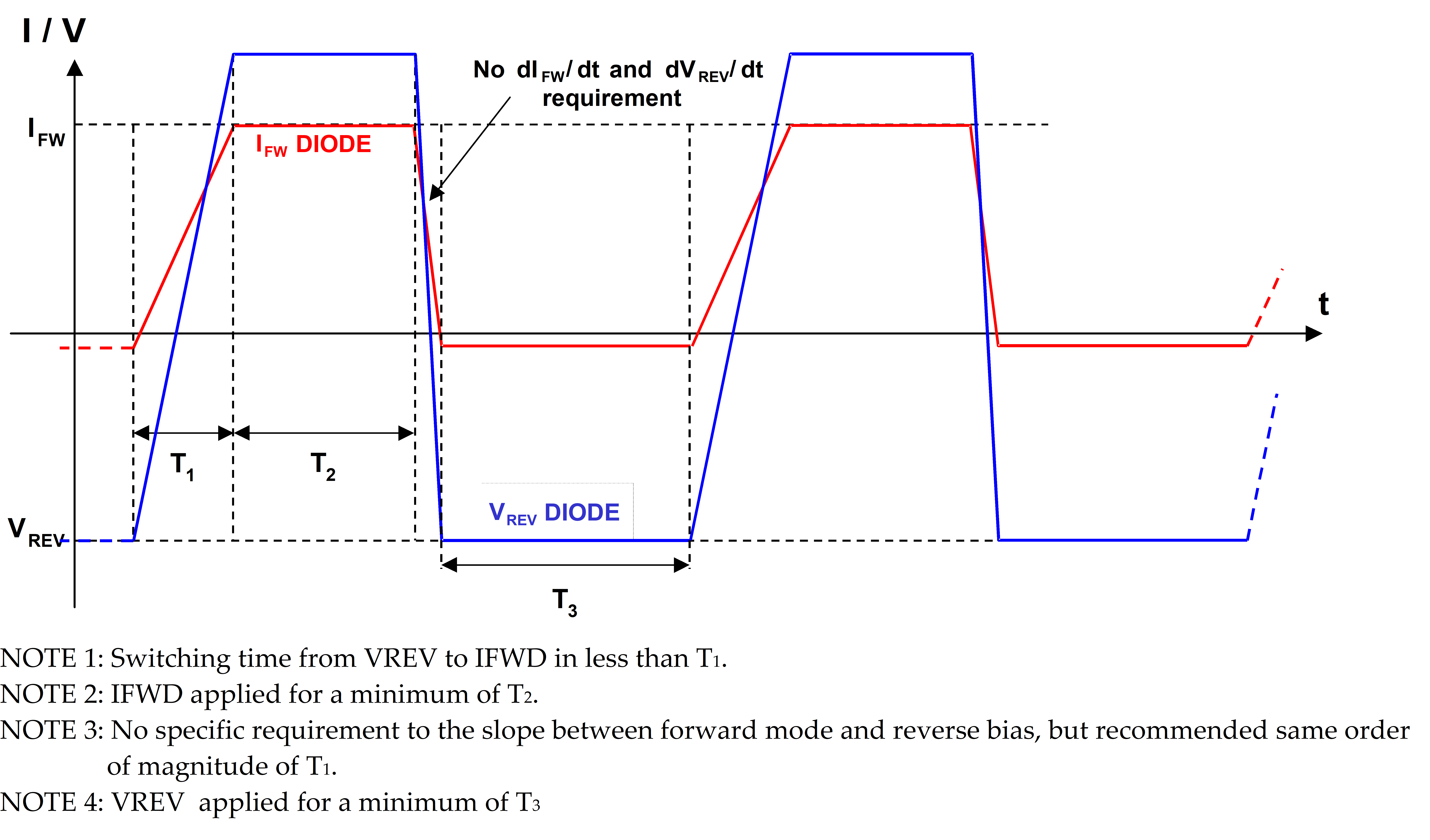 Figure 92: Diode switching test profile
Pass-fail criteria
The diode characteristics test shall satisfy the pass-fail criteria stated in the SCD-BSC or SCD-EPD.
Life test (DL)
Purpose
The purpose of this test is to determine the stability of the protection diodes under worst case operation for long duration.
Process
The protection diodes shall be equipped with interconnects
The life test shall always be preceded by a burn-in test as described in clause 9.6.6.
The duration of the life test shall be in conformance with the duration of the mission.
The long duration test shall be performed at the temperature minimum of the following two values:
- The maximum allowable temperature of the diode, to be specified in the SCD-EPD.
- The temperature corresponding to the acceleration factor applied, calculated as follows:
- Determine the activation energy Ea corresponding to a predefined level of degradation.
The activation energy can be determined experimentally by measuring τ at various temperatures above the aimed temperature or by comparison with literature data of similar degradation processes.
* Extrapolate the test temperature by using the expression:
τ (T) ~ A exp (Ea/kBT)
Where:
τ (T) = time to reach a predefined level of degradation at temperature T,
A = constant
Ea = activation energy corresponding to a predefined level of degradation,
kB = Boltzman constant
The test duration and parameter settings for each individual diode shall be as in Table 95 and mission requirements.
TableTable 95: Diode life test parameters
|
Test
|
Duration
|
Parameter
|
Requirements
|
|
Reverse Bias
|
>200 h(a)
|
VREV
|
IREV D(b) mA
|
|
Forward Bias
|
6 h(a)
|
IFW
|
VFW @ IFW < D(c) V
|
|
…
|
|
|
|
|
Reverse Bias
|
>200 h(a)
|
VREV
|
IREV D(b) mA
|
|
>200 h(a)
|
IREV 0,5xTBD(b) mA
| ||
|
Note: IREV, VREV, IFW, IREV max and IREV min are recorded values of the diode electrical parameters during Life Test.
| |||
Pass-fail criteria
The diode characteristics test shall satisfy the pass-fail criteria stated in the SCD-BSC or SCD-EPD related to IREV, VFW at IFW.
Failure definition
Failure criteria
The following shall constitute failures:
- Components that fail during subgroup tests for which the pass-fail criteria are inherent in the test method.
- Components failing to conform to the requirements of visual inspection stated in the SCD-BSC or SCD-EPD.
- Components whose marking fails to conform to the requirements of clause 9.2.3.
- Components that, when subjected to diode characteristics measurements after acceptance tests in conformance with the SCD-BSC or SCD-EPD, fail to meet one or more of the specified limits, measurement accuracy included.
Failed components
A component shall be considered to have failed if it exhibits one or more of the failure modes specified in clause 9.7.1.
Failed components shall be identified as such and included in the delivery.
Failure analysis of these components shall be performed by the supplier and the results provided to the customer as part of the NRB documentation.
For NRB, see ECSS-Q-ST-10-09.
Data documentation
The supplier shall provide a data documentation package (DDP) in conformance with Annex G for the qualification approval records and for each component delivery lot.
Delivery
All deliverable hardware specified in the order shall be delivered together with documentation in conformance with the requirements specified in clause 9.8.
One set of documents shall be sent to the customer.
Packing, despatching, handling and storage
Overview
For packaging, despatching, handling and storage of components see ESAPSS01202.
ESD sensitivity
If a protection diode is sensitive to ESD according to clause 5.2 of ESCC 23800 Issue 1 then it shall be handled and stored according to ESCC 24900 Issue 2, clause 10.
Sun simulators and calibration procedures
Sun simulators
Spectral distribution
AM0 spectrum
The AM0 reference solar spectral irradiance distribution shall be in conformance with Table 101.
- 1 This is total distribution sunlight, corresponding to an irradiance of 136,7 mW/cm² (solar constant) at AM0, on a plane surface tilted at 90° to the horizontal.
- 2 This table is based on the compilation of Christoph Wehrli, of the Physikalisch-Meteorologisches Observatorium / World Radiation Center, and is compatible with ISO 15387.
Total Irradiance of the Sun simulator
Total Irradiance (solar constant AM0-equivalent) of the Sun simulator on the test plane shall be determined by the use of AM0 calibrated reference cells as indicated in clause 10.2.
Spectral distribution of the Sun simulator
The spectral distribution of the Sun simulator light incident on the test plane normalized for 0,35 µm to 1,9 µm compared to the AM0 spectrum for the spectral regions of interest shall meet one of the classes defined in Table 102.
Percent of Total Irradiance between 0,35 µm and 1,1 µm of AM0 spectrum within various wavelength intervals defined in Table 102 shall be applied for Silicon and GaAs single junction solar cells.
TableTable 101: AM0 solar spectral irradiance (WRC)
|
[nm]
|
E[W/m²/nm]
|
[nm]
|
E[W/m²/nm]
|
[nm]
|
E[W/m²/nm]
|
[nm]
|
E[W/m²/nm]
|
|
199.5
|
0.005
|
245.5
|
0.051
|
291.5
|
0.600
|
320.8
|
0.844
|
|
200.5
|
0.007
|
246.5
|
0.051
|
292.5
|
0.545
|
321.2
|
0.847
|
|
201.5
|
0.007
|
247.5
|
0.057
|
293.5
|
0.545
|
321.6
|
0.736
|
|
202.5
|
0.008
|
248.5
|
0.045
|
294.5
|
0.509
|
322
|
0.695
|
|
203.5
|
0.009
|
249.5
|
0.058
|
295.5
|
0.548
|
322.4
|
0.773
|
|
204.5
|
0.009
|
250.5
|
0.059
|
296.5
|
0.492
|
322.8
|
0.758
|
|
205.5
|
0.010
|
251.5
|
0.047
|
297.5
|
0.531
|
323.2
|
0.646
|
|
206.5
|
0.010
|
252.5
|
0.044
|
298.5
|
0.413
|
323.6
|
0.603
|
|
207.5
|
0.011
|
253.5
|
0.055
|
299.5
|
0.485
|
324
|
0.604
|
|
208.5
|
0.015
|
254.5
|
0.061
|
300.5
|
0.403
|
324.4
|
0.618
|
|
209.5
|
0.024
|
255.5
|
0.089
|
301.5
|
0.445
|
324.8
|
0.654
|
|
210.5
|
0.028
|
256.5
|
0.107
|
302.5
|
0.484
|
325.2
|
0.646
|
|
211.5
|
0.034
|
257.5
|
0.129
|
303.5
|
0.631
|
325.6
|
0.682
|
|
212.5
|
0.030
|
258.5
|
0.134
|
304.5
|
0.610
|
326
|
0.852
|
|
213.5
|
0.032
|
259.5
|
0.108
|
305.5
|
0.580
|
326.4
|
1.049
|
|
214.5
|
0.041
|
260.5
|
0.102
|
306.5
|
0.575
|
326.8
|
1.111
|
|
215.5
|
0.037
|
261.5
|
0.103
|
307.5
|
0.645
|
327.2
|
1.108
|
|
216.5
|
0.034
|
262.5
|
0.121
|
308.5
|
0.613
|
327.6
|
1.050
|
|
217.5
|
0.036
|
263.5
|
0.175
|
309.5
|
0.484
|
328
|
0.965
|
|
218.5
|
0.045
|
264.5
|
0.274
|
310
|
0.495
|
328.4
|
0.914
|
|
219.5
|
0.048
|
265.5
|
0.280
|
310.4
|
0.507
|
328.8
|
0.913
|
|
220.5
|
0.048
|
266.5
|
0.260
|
310.8
|
0.588
|
329.2
|
0.952
|
|
221.5
|
0.039
|
267.5
|
0.270
|
311.2
|
0.707
|
329.6
|
1.043
|
|
222.5
|
0.051
|
268.5
|
0.260
|
311.6
|
0.747
|
330
|
1.144
|
|
223.5
|
0.066
|
269.5
|
0.252
|
312
|
0.707
|
330.4
|
1.137
|
|
224.5
|
0.058
|
270.5
|
0.293
|
312.4
|
0.644
|
330.5
|
1.006
|
|
225.5
|
0.054
|
271.5
|
0.232
|
312.8
|
0.663
|
331.5
|
0.968
|
|
226.5
|
0.041
|
272.5
|
0.215
|
313.2
|
0.710
|
332.5
|
0.921
|
|
227.5
|
0.041
|
273.5
|
0.204
|
313.6
|
0.691
|
333.5
|
0.905
|
|
228.5
|
0.054
|
274.5
|
0.137
|
314
|
0.689
|
334.5
|
0.940
|
|
229.5
|
0.048
|
275.5
|
0.200
|
314.4
|
0.722
|
335.5
|
0.982
|
|
230.5
|
0.056
|
276.5
|
0.258
|
314.8
|
0.673
|
336.5
|
0.765
|
|
231.5
|
0.050
|
277.5
|
0.240
|
315.2
|
0.695
|
337.5
|
0.866
|
|
232.5
|
0.055
|
278.5
|
0.166
|
315.6
|
0.765
|
338.5
|
0.916
|
|
233.5
|
0.046
|
279.5
|
0.089
|
316
|
0.675
|
339.5
|
0.937
|
|
234.5
|
0.039
|
280.5
|
0.112
|
316.4
|
0.569
|
340.5
|
0.992
|
|
235.5
|
0.057
|
281.5
|
0.231
|
316.8
|
0.623
|
341.5
|
0.936
|
|
236.5
|
0.049
|
282.5
|
0.307
|
317.2
|
0.749
|
342.5
|
0.995
|
|
237.5
|
0.053
|
283.5
|
0.330
|
317.6
|
0.830
|
343.5
|
0.985
|
|
238.5
|
0.042
|
284.5
|
0.244
|
318
|
0.813
|
344.5
|
0.719
|
|
239.5
|
0.046
|
285.5
|
0.141
|
318.4
|
0.673
|
345.5
|
0.967
|
|
240.5
|
0.043
|
286.5
|
0.320
|
318.8
|
0.642
|
346.5
|
0.919
|
|
241.5
|
0.052
|
287.5
|
0.371
|
319.2
|
0.768
|
347.5
|
0.902
|
|
242.5
|
0.072
|
288.5
|
0.307
|
319.6
|
0.759
|
348.5
|
0.948
|
|
243.5
|
0.065
|
289.5
|
0.456
|
320
|
0.712
|
349.5
|
0.865
|
|
244.5
|
0.062
|
290.5
|
0.623
|
320.4
|
0.778
|
350.5
|
1.119
|
TableTable 101: AM0 solar spectral irradiance (WRC) (continued)
|
[nm]
|
E[W/m²/nm]
|
[nm]
|
E[W/m²/nm]
|
[nm]
|
E[W/m²/nm]
|
[nm]
|
E[W/m²/nm]
|
|
351.5
|
0.993
|
397.5
|
1.040
|
443.5
|
1.911
|
489.5
|
1.962
|
|
352.5
|
0.871
|
398.5
|
1.538
|
444.5
|
1.975
|
490.5
|
2.009
|
|
353.5
|
1.115
|
399.5
|
1.655
|
445.5
|
1.823
|
491.5
|
1.898
|
|
354.5
|
1.133
|
400.5
|
1.649
|
446.5
|
1.893
|
492.5
|
1.898
|
|
355.5
|
1.058
|
401.5
|
1.796
|
447.5
|
2.079
|
493.5
|
1.890
|
|
356.5
|
0.938
|
402.5
|
1.803
|
448.5
|
1.975
|
494.5
|
2.060
|
|
357.5
|
0.891
|
403.5
|
1.658
|
449.5
|
2.029
|
495.5
|
1.928
|
|
358.5
|
0.627
|
404.5
|
1.602
|
450.5
|
2.146
|
496.5
|
2.019
|
|
359.5
|
1.136
|
405.5
|
1.672
|
451.5
|
2.111
|
497.5
|
2.020
|
|
360.5
|
0.979
|
406.5
|
1.624
|
452.5
|
1.943
|
498.5
|
1.868
|
|
361.5
|
0.894
|
407.5
|
1.545
|
453.5
|
1.972
|
499.5
|
1.972
|
|
362.5
|
1.175
|
408.5
|
1.824
|
454.5
|
1.981
|
500.5
|
1.859
|
|
363.5
|
0.958
|
409.5
|
1.706
|
455.5
|
2.036
|
501.5
|
1.814
|
|
364.5
|
1.015
|
410.5
|
1.502
|
456.5
|
2.079
|
502.5
|
1.896
|
|
365.5
|
1.263
|
411.5
|
1.819
|
457.5
|
2.102
|
503.5
|
1.936
|
|
366.5
|
1.249
|
412.5
|
1.791
|
458.5
|
1.973
|
504.5
|
1.871
|
|
367.5
|
1.214
|
413.5
|
1.758
|
459.5
|
2.011
|
505.5
|
1.995
|
|
368.5
|
1.088
|
414.5
|
1.739
|
460.5
|
2.042
|
506.5
|
1.963
|
|
369.5
|
1.331
|
415.5
|
1.736
|
461.5
|
2.057
|
507.5
|
1.908
|
|
370.5
|
1.075
|
416.5
|
1.844
|
462.5
|
2.106
|
508.5
|
1.921
|
|
371.5
|
1.307
|
417.5
|
1.667
|
463.5
|
2.042
|
509.5
|
1.918
|
|
372.5
|
1.065
|
418.5
|
1.686
|
464.5
|
1.978
|
510.5
|
1.949
|
|
373.5
|
0.838
|
419.5
|
1.703
|
465.5
|
2.044
|
511.5
|
1.999
|
|
374.5
|
0.878
|
420.5
|
1.760
|
466.5
|
1.923
|
512.5
|
1.869
|
|
375.5
|
1.141
|
421.5
|
1.799
|
467.5
|
2.017
|
513.5
|
1.863
|
|
376.5
|
1.101
|
422.5
|
1.584
|
468.5
|
1.996
|
514.5
|
1.876
|
|
377.5
|
1.291
|
423.5
|
1.713
|
469.5
|
1.992
|
515.5
|
1.902
|
|
378.5
|
1.341
|
424.5
|
1.770
|
470.5
|
1.879
|
516.5
|
1.671
|
|
379.5
|
1.000
|
425.5
|
1.697
|
471.5
|
2.020
|
517.5
|
1.728
|
|
380.5
|
1.289
|
426.5
|
1.700
|
472.5
|
2.043
|
518.5
|
1.656
|
|
381.5
|
1.096
|
427.5
|
1.571
|
473.5
|
1.993
|
519.5
|
1.830
|
|
382.5
|
0.733
|
428.5
|
1.589
|
474.5
|
2.053
|
520.5
|
1.833
|
|
383.5
|
0.684
|
429.5
|
1.477
|
475.5
|
2.018
|
521.5
|
1.908
|
|
384.5
|
1.027
|
430.5
|
1.136
|
476.5
|
1.958
|
522.5
|
1.825
|
|
385.5
|
0.954
|
431.5
|
1.688
|
477.5
|
2.077
|
523.5
|
1.896
|
|
386.5
|
1.071
|
432.5
|
1.648
|
478.5
|
2.011
|
524.5
|
1.960
|
|
387.5
|
0.966
|
433.5
|
1.733
|
479.5
|
2.078
|
525.5
|
1.932
|
|
388.5
|
0.912
|
434.5
|
1.672
|
480.5
|
2.037
|
526.5
|
1.676
|
|
389.5
|
1.227
|
435.5
|
1.725
|
481.5
|
2.092
|
527.5
|
1.830
|
|
390.5
|
1.223
|
436.5
|
1.931
|
482.5
|
2.025
|
528.5
|
1.899
|
|
391.5
|
1.398
|
437.5
|
1.808
|
483.5
|
2.021
|
529.5
|
1.920
|
|
392.5
|
0.955
|
438.5
|
1.569
|
484.5
|
1.971
|
530.5
|
1.954
|
|
393.5
|
0.489
|
439.5
|
1.827
|
485.5
|
1.832
|
531.5
|
1.965
|
|
394.5
|
1.101
|
440.5
|
1.715
|
486.5
|
1.627
|
532.5
|
1.773
|
|
395.5
|
1.378
|
441.5
|
1.933
|
487.5
|
1.832
|
533.5
|
1.925
|
|
396.5
|
0.650
|
442.5
|
1.982
|
488.5
|
1.916
|
534.5
|
1.860
|
TableTable 101: AM0 solar spectral irradiance (WRC) (continued)
|
[nm]
|
E[W/m²/nm]
|
[nm]
|
E[W/m²/nm]
|
[nm]
|
E[W/m²/nm]
|
[nm]
|
E[W/m²/nm]
|
|
535.5
|
1.992
|
581.5
|
1.855
|
627.5
|
1.699
|
717
|
1.355
|
|
536.5
|
1.873
|
582.5
|
1.875
|
628.5
|
1.699
|
719
|
1.329
|
|
537.5
|
1.884
|
583.5
|
1.859
|
629.5
|
1.679
|
721
|
1.332
|
|
538.5
|
1.906
|
584.5
|
1.862
|
631
|
1.641
|
723
|
1.349
|
|
539.5
|
1.834
|
585.5
|
1.786
|
633
|
1.653
|
725.9
|
1.351
|
|
540.5
|
1.772
|
586.5
|
1.832
|
635
|
1.658
|
727
|
1.347
|
|
541.5
|
1.883
|
587.5
|
1.850
|
637
|
1.656
|
729
|
1.320
|
|
542.5
|
1.827
|
588.5
|
1.752
|
639
|
1.653
|
731
|
1.327
|
|
543.5
|
1.881
|
589.5
|
1.614
|
641
|
1.616
|
733
|
1.319
|
|
544.5
|
1.881
|
590.5
|
1.815
|
643
|
1.623
|
735.9
|
1.310
|
|
545.5
|
1.903
|
591.5
|
1.789
|
645
|
1.629
|
737
|
1.308
|
|
546.5
|
1.881
|
592.5
|
1.810
|
647
|
1.605
|
739
|
1.279
|
|
547.5
|
1.835
|
593.5
|
1.798
|
649
|
1.560
|
741
|
1.259
|
|
548.5
|
1.865
|
594.5
|
1.776
|
651
|
1.608
|
743
|
1.287
|
|
549.5
|
1.897
|
595.5
|
1.785
|
653
|
1.601
|
745
|
1.280
|
|
550.5
|
1.864
|
596.5
|
1.807
|
655
|
1.534
|
747
|
1.284
|
|
551.5
|
1.873
|
597.5
|
1.783
|
657
|
1.386
|
749
|
1.271
|
|
552.5
|
1.848
|
598.5
|
1.760
|
659
|
1.551
|
751
|
1.263
|
|
553.5
|
1.884
|
599.5
|
1.777
|
661
|
1.573
|
753
|
1.260
|
|
554.5
|
1.900
|
600.5
|
1.748
|
663
|
1.557
|
755
|
1.256
|
|
555.5
|
1.899
|
601.5
|
1.753
|
665
|
1.562
|
757
|
1.249
|
|
556.5
|
1.823
|
602.5
|
1.721
|
667
|
1.537
|
759
|
1.241
|
|
557.5
|
1.848
|
603.5
|
1.789
|
669
|
1.548
|
761
|
1.238
|
|
558.5
|
1.789
|
604.5
|
1.779
|
671
|
1.518
|
763
|
1.242
|
|
559.5
|
1.810
|
605.5
|
1.766
|
673
|
1.523
|
765
|
1.222
|
|
560.5
|
1.845
|
606.5
|
1.762
|
675
|
1.512
|
767
|
1.186
|
|
561.5
|
1.826
|
607.5
|
1.760
|
677
|
1.510
|
769
|
1.204
|
|
562.5
|
1.852
|
608.5
|
1.745
|
679
|
1.500
|
771
|
1.205
|
|
563.5
|
1.863
|
609.5
|
1.746
|
681
|
1.494
|
773
|
1.209
|
|
564.5
|
1.856
|
610.5
|
1.705
|
683
|
1.481
|
775
|
1.189
|
|
565.5
|
1.800
|
611.5
|
1.748
|
685.9
|
1.457
|
777
|
1.197
|
|
566.5
|
1.831
|
612.5
|
1.707
|
687
|
1.469
|
779
|
1.188
|
|
567.5
|
1.889
|
613.5
|
1.685
|
689
|
1.463
|
781
|
1.188
|
|
568.5
|
1.812
|
614.5
|
1.715
|
691
|
1.450
|
783
|
1.177
|
|
569.5
|
1.862
|
615.5
|
1.715
|
693
|
1.450
|
785
|
1.181
|
|
570.5
|
1.772
|
616.5
|
1.611
|
695.9
|
1.438
|
787
|
1.178
|
|
571.5
|
1.825
|
617.5
|
1.709
|
697
|
1.418
|
789
|
1.175
|
|
572.5
|
1.894
|
618.5
|
1.726
|
699
|
1.427
|
791
|
1.159
|
|
573.5
|
1.878
|
619.5
|
1.709
|
701
|
1.388
|
793
|
1.144
|
|
574.5
|
1.869
|
620.5
|
1.736
|
703
|
1.390
|
795
|
1.135
|
|
575.5
|
1.832
|
621.5
|
1.692
|
705.9
|
1.417
|
797
|
1.153
|
|
576.5
|
1.848
|
622.5
|
1.715
|
707
|
1.402
|
799
|
1.136
|
|
577.5
|
1.859
|
623.5
|
1.668
|
709
|
1.386
|
801
|
1.143
|
|
578.5
|
1.786
|
624.5
|
1.658
|
711
|
1.387
|
803
|
1.130
|
|
579.5
|
1.830
|
625.5
|
1.634
|
713
|
1.375
|
805.9
|
1.116
|
|
580.5
|
1.840
|
626.5
|
1.699
|
715.9
|
1.368
|
807
|
1.121
|
TableTable 101: AM0 solar spectral irradiance (WRC) (continued)
|
[nm]
|
E[W/m²/nm]
|
[nm]
|
E[W/m²/nm]
|
[nm]
|
E[W/m²/nm]
|
[nm]
|
E[W/m²/nm]
|
|
809
|
1.096
|
901
|
0.905
|
993
|
0.755
|
1212.5
|
0.489
|
|
811
|
1.115
|
903
|
0.905
|
995.9
|
0.756
|
1217.5
|
0.500
|
|
813
|
1.116
|
905
|
0.893
|
997
|
0.743
|
1222.5
|
0.481
|
|
815.9
|
1.108
|
907
|
0.891
|
999
|
0.743
|
1227.5
|
0.481
|
|
817
|
1.105
|
909
|
0.861
|
1002.5
|
0.745
|
1232.5
|
0.484
|
|
819
|
1.065
|
911
|
0.870
|
1007.5
|
0.737
|
1237.5
|
0.477
|
|
821
|
1.081
|
913
|
0.876
|
1012.5
|
0.734
|
1242.5
|
0.477
|
|
823
|
1.074
|
915
|
0.866
|
1017.5
|
0.721
|
1247.5
|
0.466
|
|
825.9
|
1.076
|
917
|
0.859
|
1022.5
|
0.704
|
1252.5
|
0.474
|
|
827
|
1.077
|
919
|
0.858
|
1027.5
|
0.708
|
1257.5
|
0.463
|
|
829
|
1.073
|
921
|
0.830
|
1032.5
|
0.688
|
1262.5
|
0.444
|
|
831
|
1.069
|
923
|
0.821
|
1037.5
|
0.692
|
1267.5
|
0.438
|
|
833
|
1.034
|
925
|
0.825
|
1042.5
|
0.681
|
1272.5
|
0.439
|
|
835.9
|
1.053
|
927
|
0.828
|
1047.5
|
0.685
|
1277.5
|
0.453
|
|
837
|
1.052
|
929
|
0.833
|
1052.5
|
0.661
|
1282.5
|
0.435
|
|
839
|
1.042
|
931
|
0.826
|
1057.5
|
0.650
|
1287.5
|
0.437
|
|
841
|
1.045
|
933
|
0.832
|
1062.5
|
0.642
|
1292.5
|
0.442
|
|
843
|
1.028
|
935.9
|
0.818
|
1067.5
|
0.643
|
1297.5
|
0.438
|
|
845.9
|
1.033
|
937
|
0.802
|
1072.5
|
0.638
|
1302.5
|
0.438
|
|
847
|
1.025
|
939
|
0.808
|
1077.5
|
0.630
|
1307.5
|
0.429
|
|
849
|
0.971
|
941
|
0.800
|
1082.5
|
0.620
|
1312.5
|
0.419
|
|
851
|
1.003
|
943
|
0.784
|
1087.5
|
0.614
|
1317.5
|
0.416
|
|
853
|
0.973
|
945.9
|
0.799
|
1092.5
|
0.612
|
1322.5
|
0.416
|
|
855.9
|
0.877
|
947
|
0.793
|
1097.5
|
0.599
|
1327.5
|
0.411
|
|
857
|
1.011
|
949
|
0.777
|
1102.5
|
0.608
|
1332.5
|
0.405
|
|
859
|
0.997
|
951
|
0.778
|
1107.5
|
0.601
|
1337.5
|
0.400
|
|
861
|
0.997
|
953
|
0.771
|
1112.5
|
0.603
|
1342.5
|
0.398
|
|
863
|
0.999
|
955.9
|
0.760
|
1117.5
|
0.589
|
1347.5
|
0.394
|
|
865.9
|
0.970
|
957
|
0.774
|
1122.5
|
0.579
|
1352.5
|
0.387
|
|
867
|
0.880
|
959
|
0.771
|
1127.5
|
0.569
|
1357.5
|
0.382
|
|
869
|
0.967
|
961
|
0.767
|
1132.5
|
0.566
|
1362.5
|
0.378
|
|
871
|
0.986
|
963
|
0.767
|
1137.5
|
0.563
|
1367.5
|
0.370
|
|
873
|
0.978
|
965.9
|
0.764
|
1142.5
|
0.557
|
1372.5
|
0.369
|
|
875.9
|
0.981
|
967
|
0.757
|
1147.5
|
0.556
|
1377.5
|
0.368
|
|
877
|
0.984
|
969
|
0.776
|
1152.5
|
0.545
|
1382.5
|
0.364
|
|
879
|
0.959
|
971
|
0.763
|
1157.5
|
0.554
|
1387.5
|
0.364
|
|
881
|
0.960
|
973
|
0.764
|
1162.5
|
0.540
|
1392.5
|
0.358
|
|
883
|
0.948
|
975.9
|
0.750
|
1167.5
|
0.530
|
1397.5
|
0.357
|
|
885
|
0.963
|
977
|
0.768
|
1172.5
|
0.533
|
1402.5
|
0.353
|
|
887
|
0.947
|
979
|
0.768
|
1177.5
|
0.525
|
1407.5
|
0.350
|
|
889
|
0.949
|
981
|
0.762
|
1182.5
|
0.514
|
1412.5
|
0.346
|
|
891
|
0.944
|
983
|
0.766
|
1187.5
|
0.512
|
1417.5
|
0.344
|
|
893
|
0.934
|
985.9
|
0.771
|
1192.5
|
0.511
|
1422.5
|
0.343
|
|
895
|
0.936
|
987
|
0.756
|
1197.5
|
0.502
|
1427.5
|
0.348
|
|
897
|
0.939
|
989
|
0.767
|
1202.5
|
0.496
|
1432.5
|
0.337
|
|
899
|
0.912
|
991
|
0.764
|
1207.5
|
0.494
|
1437.5
|
0.331
|
TableTable 101: AM0 solar spectral irradiance (WRC) (continued)
|
[nm]
|
E[W/m²/nm]
|
[nm]
|
E[W/m²/nm]
|
[nm]
|
E[W/m²/nm]
|
[nm]
|
E[W/m²/nm]
|
|
1442.5
|
0.327
|
1672.5
|
0.228
|
1902.5
|
0.133
|
2402.5
|
0.054
|
|
1447.5
|
0.318
|
1677.5
|
0.220
|
1907.5
|
0.136
|
2422.5
|
0.057
|
|
1452.5
|
0.323
|
1682.5
|
0.221
|
1912.5
|
0.138
|
2442.5
|
0.051
|
|
1457.5
|
0.307
|
1687.5
|
0.219
|
1917.5
|
0.136
|
2467.5
|
0.053
|
|
1462.5
|
0.317
|
1692.5
|
0.219
|
1922.5
|
0.134
|
2492.5
|
0.054
|
|
1467.5
|
0.311
|
1697.5
|
0.214
|
1927.5
|
0.132
|
2517.5
|
0.047
|
|
1472.5
|
0.311
|
1702.5
|
0.217
|
1932.5
|
0.132
|
2542.5
|
0.046
|
|
1477.5
|
0.307
|
1707.5
|
0.212
|
1937.5
|
0.131
|
2567.5
|
0.044
|
|
1482.5
|
0.303
|
1712.5
|
0.203
|
1942.5
|
0.129
|
2592.5
|
0.042
|
|
1487.5
|
0.298
|
1717.5
|
0.212
|
1947.5
|
0.127
|
2617.5
|
0.041
|
|
1492.5
|
0.303
|
1722.5
|
0.205
|
1952.5
|
0.126
|
2642.5
|
0.039
|
|
1497.5
|
0.300
|
1727.5
|
0.196
|
1957.5
|
0.122
|
2672.5
|
0.038
|
|
1502.5
|
0.296
|
1732.5
|
0.190
|
1962.5
|
0.126
|
2702.5
|
0.036
|
|
1507.5
|
0.295
|
1737.5
|
0.189
|
1967.5
|
0.125
|
2732.5
|
0.035
|
|
1512.5
|
0.290
|
1742.5
|
0.191
|
1972.5
|
0.125
|
2762.5
|
0.034
|
|
1517.5
|
0.290
|
1747.5
|
0.185
|
1977.5
|
0.129
|
2797.5
|
0.032
|
|
1522.5
|
0.286
|
1752.5
|
0.187
|
1982.5
|
0.125
|
2832.5
|
0.031
|
|
1527.5
|
0.290
|
1757.5
|
0.189
|
1987.5
|
0.123
|
2867.5
|
0.029
|
|
1532.5
|
0.282
|
1762.5
|
0.184
|
1992.5
|
0.121
|
2907.5
|
0.028
|
|
1537.5
|
0.274
|
1767.5
|
0.182
|
1997.5
|
0.123
|
2947.5
|
0.026
|
|
1542.5
|
0.275
|
1772.5
|
0.177
|
2002.5
|
0.116
|
2987.5
|
0.025
|
|
1547.5
|
0.274
|
1777.5
|
0.173
|
2012.5
|
0.114
|
3025
|
0.024
|
|
1552.5
|
0.273
|
1782.5
|
0.171
|
2022.5
|
0.113
|
3075
|
0.023
|
|
1557.5
|
0.272
|
1787.5
|
0.170
|
2032.5
|
0.110
|
3125
|
0.021
|
|
1562.5
|
0.269
|
1792.5
|
0.169
|
2042.5
|
0.107
|
3175
|
0.020
|
|
1567.5
|
0.263
|
1797.5
|
0.173
|
2052.5
|
0.104
|
3235
|
0.019
|
|
1572.5
|
0.260
|
1802.5
|
0.169
|
2062.5
|
0.100
|
3295
|
0.018
|
|
1577.5
|
0.259
|
1807.5
|
0.168
|
2077.5
|
0.101
|
3355
|
0.016
|
|
1582.5
|
0.255
|
1812.5
|
0.160
|
2092.5
|
0.098
|
3425
|
0.015
|
|
1587.5
|
0.252
|
1817.5
|
0.160
|
2107.5
|
0.093
|
3495
|
0.014
|
|
1592.5
|
0.246
|
1822.5
|
0.159
|
2122.5
|
0.087
|
3575
|
0.013
|
|
1597.5
|
0.246
|
1827.5
|
0.156
|
2137.5
|
0.085
|
3665
|
0.012
|
|
1602.5
|
0.247
|
1832.5
|
0.156
|
2152.5
|
0.081
|
3755
|
0.011
|
|
1607.5
|
0.242
|
1837.5
|
0.150
|
2167.5
|
0.080
|
3855
|
0.010
|
|
1612.5
|
0.244
|
1842.5
|
0.153
|
2182.5
|
0.075
|
3965
|
0.009
|
|
1617.5
|
0.243
|
1847.5
|
0.151
|
2197.5
|
0.073
|
4085
|
0.008
|
|
1622.5
|
0.240
|
1852.5
|
0.148
|
2212.5
|
0.075
|
4225
|
0.007
|
|
1627.5
|
0.244
|
1857.5
|
0.145
|
2227.5
|
0.075
|
4385
|
0.006
|
|
1632.5
|
0.241
|
1862.5
|
0.143
|
2247.5
|
0.072
|
4575
|
0.005
|
|
1637.5
|
0.237
|
1867.5
|
0.143
|
2262.5
|
0.071
|
4805
|
0.004
|
|
1642.5
|
0.234
|
1872.5
|
0.135
|
2282.5
|
0.069
|
5085
|
0.003
|
|
1647.5
|
0.235
|
1877.5
|
0.135
|
2302.5
|
0.066
|
5445
|
0.002
|
|
1652.5
|
0.234
|
1882.5
|
0.140
|
2322.5
|
0.053
|
5925
|
0.002
|
|
1657.5
|
0.234
|
1887.5
|
0.138
|
2342.5
|
0.058
|
6615
|
0.001
|
|
1662.5
|
0.233
|
1892.5
|
0.137
|
2362.5
|
0.065
|
7785
|
0.001
|
|
1667.5
|
0.229
|
1897.5
|
0.138
|
2382.5
|
0.055
|
10075
|
0.000
|
TableTable 102: Classes of single and multi-source solar simulators
|
Wavelength Interval[µm]
|
Percent of Total Irradiance for between indicated Total Range
|
Bins
|
Class A
|
Class B
|
Class C
| |
|
Total Range
|
Total Range
| |||||
|
0,35 - 0,4
|
4,4
|
5,6
|
0,15
|
15 %
|
20 %
|
25 %
|
|
0,4 - 0,5
|
15,3
|
19,4
| ||||
|
0,5 - 0,6
|
15,2
|
19,3
|
0,1
|
15 %
|
20 %
|
25 %
|
|
0,6 - 0,7
|
13,1
|
16,6
| ||||
|
0,7 - 0,8
|
10,4
|
13,2
| ||||
|
0,8 - 0,9
|
8,4
|
10,6
| ||||
|
0,9 - 1,0
|
6,6
|
8,3
| ||||
|
1,0 - 1,1
|
5,5
|
7,0
| ||||
|
1,1 - 1,2
|
4,5
|
|
0,2
|
15 %
|
20 %
|
25 %
|
|
1,2 - 1,3
|
3,8
|
|
||||
|
1,3 - 1,4
|
3,2
|
|
||||
|
1,4 - 1,5
|
2,7
|
|
||||
|
1,5 - 1,6
|
2,2
|
|
||||
|
1,6 - 1,7
|
1,9
|
|
||||
|
1,7 - 1,8
|
1,6
|
|
||||
|
1,8 - 1,9
|
1,2
|
|
||||
The following method shall be used to verify spectral distribution of irradiance performance:
- Apply one of the following methods: Direct measurement with a calibrated spectro-radiometer.
Measurement with a two-channel spectro-radiometer against a calibrated reference light source.
- Calculate the deviation of the total energy per spectral region with reference to the AM0 spectrum using the following expression:
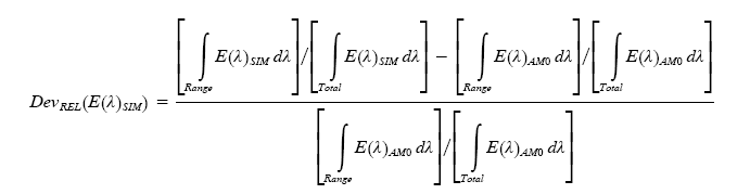 where
where
E(λ)SIM is the spectral irradiance of the solar simulator;
E(λ)AM0 is the AM0 spectral irradiance;
Range is the spectral region of interest.
For a test lot of single solar cells, the spectral distribution of the Sun simulator in the test plane shall be matched to the AM0 spectrum for errors due to the spectral response spread of the relevant lot of cells to be 1 % or less, as follows:
- Measure the short-circuit current of 10 solar cells accepted by the customer as representing a worst-case simulation of the spectral response spread of the cells to be tested, at the constant nominal intensity of the Sun simulator.
- From the measured spectral response of the cells (in conformance with clause 7.5.5) and the AM0 spectrum given in Table 101:
- Calculate the short-circuit current and multiply it by a common factor which adjusts the average calculated short-circuit current to the average current resulting from the simulator measurements.
- Ensure that the difference between the calculated and measured current of each individual cell does not exceed 1 % of the measured current.
For a test lot of multijunction solar cells, the spectral distribution of the Sun simulator in the test plane shall be matched to the AM0 spectrum for errors due to the spectral response spread of the relevant lot of cells to be 1 % or less, as follows:
- Adjust the irradiance in the test plane to AM0 equivalent conditions using component reference cells
- Measure the spectral distribution of the Sun simulator following one of the methods given in 10.1.1.2a.
- Measure the spectral response of 10 solar cells accepted by the customer as representing a worst-case simulation of the spectral response spread of the cells to be tested, according to clause 7.5.5.
- From the measured spectral responses of the cells and the component reference cell, the spectral distribution of the Sun simulator and the AM0 spectrum given in Table 101:
- Calculate the spectral mismatch parameter for each junction.
- Ensure that the effective irradiance (i.e. short-circuit output under the Sun simulator divided by AM0 calibrated value) for each component reference cell multiply by the corresponding individual spectral mismatch parameter is 1,00 0,01.
Irradiance uniformity
The uniformity of the irradiance, as defined in requirement 10.1.2e, in the test plane over the full extent of the nominated test area, shall meet one of the classes of solar simulators in Table 103.
For multi-source simulators used for characterizing multijunction solar cells, the relevant class of solar simulator in Table 103 shall be determined for each junction.
For bare solar cells and SCAs, testing, the largest dimension of the detector shall be less than half of the smallest dimensions of the cell, with a minimum dimension of for rectangular detector, or a minimum area of 1cm² for circular detector.
In the case of coupons, the detector shall not be bigger than the SCAs bonded to it.
The nonconformity in the uniformity of the irradiance shall be calculated as follows:
Nonconformity (%) = 100 x (MI − mI)/(MI + mI)
Where:
MI = Maximum irradiance,
mI = Minimum irradiance,
With the maximum and minimum irradiance measured with the detectors over the nominated test area (corrected for temporal instability).
TableTable 103: Classes of solar simulators with respect to nonconformity of irradiance uniformity
|
Class
|
Class A
|
Class B
|
Class C
|
|
Nonconformity (%)
|
2
|
5
|
10
|
The irradiance uniformity of the Sun simulator in the test plane shall not introduce errors due to the positioning accuracy of the relevant cells higher than 1 % or other value proposed by the supplier and accepted by the customer.
The irradiance uniformity of the Sun simulator in the test area shall not introduce errors due to the dimension of the reference cell used to adjust Sun simulator irradiance to AM0 equivalent conditions higher than 1 % or other value proposed by the supplier and accepted by the customer.
See clause 10.2 for requirements of reference solar cells.
Irradiance stability
For the regular time interval of data acquisition of a particular test the irradiance, shall be stable to the degree specified for one of the corresponding class of solar simulator in Table 104.
See requirement 10.2.6.1c for solar simulator verification.
For multi-source simulators used for characterizing multijunction solar cells, the relevant class of solar simulator in Table 104 shall be determined for each junction.
The temporal (the time in between two consecutive calibrations of the solar simulator) instability shall be calculated with the following expression:
Temporal instability (%) = 100 x (MI − mI) / (MI + mI)
Where :
MI = Maximum irradiance,
mI = minimum irradiance
with the maximum and minimum irradiance measured with the detector at any particular point of the nominated test area plane during the time of data acquisition.
TableTable 104: Classes of solar simulators with respect to temporal instability of irradiance
|
Class
|
Class A
|
Class B
|
Class C
|
|
Nonconformity (%)
|
1
|
5
|
10
|
The irradiance stability of the Sun simulator in the test plane shall be capable to guarantee reproducibility and, thus, not introduce errors on measured solar cell electrical parameters (Isc, Voc, and Pmax) higher than 1 % or other value proposed by the supplier and accepted by the customer.
Standard cell and Sun simulator calibration
Primary standards
Single junction or component primary standard cells, calibrated using a method defined in ISO 15387:2005, shall be used for setting light sources to standard illumination conditions.
The number and type of primary standard cells shall be mutually agreed upon between the supplier and the customer.
Secondary working standards (SWS)
Selection of secondary working standards
For single junctions, 10 solar cells representing a spectral response range similar when compared in conformance with requirement 10.2.2.1d to that of the cells to be tested, shall be calibrated for their AM0 equivalent short-circuit current using a Sun simulator, conforming to clause 10.1, using the accepted primary standards
For multi-junctions, three sets of component solar cells representing a spectral response range similar when compared in conformance with requirement 10.2.2.1d to the cells to be tested, shall be calibrated for their AM0 equivalent short-circuit current using a multi-source solar simulator, conforming to clause 10.1, using the accepted primary standards.
Cells shall be matched in its size to the cells under test.
The comparison method shall be agreed with the customer.
Irradiated secondary working standards
Electron or proton irradiated secondary working standards shall be calibrated to adjust solar simulator irradiance at the test plane to AM0 equivalent intensity when measuring the electrical performance of bare cells or SCAs irradiated with the same dose and particle energy.
The number of irradiated SWS shall be agreed between the supplier and the customer.
Secondary working standards performance requirements
Visual inspection requirements.
SWS shall meet visual inspection requirements on defects (clauses 7.5.1.4 and 7.5.1.5 for bare solar cells, or clause 6.4.3.1 for SCA’s).
Any deviation from the visual inspection requirements on defects shall:
- not affect performance or reliability,
- be agreed with the customer, and
- be justified.
Stability of the sensitivity
The stability of the sensitivity of the SWS under operating conditions shall be verified by comparing the short-circuit current of five of the SWS before and after a photon-irradiation test with the short-circuit current of the remaining five SWS which are kept in the dark.
If the average short-circuit current of the photon-irradiated cells deviates by more than 1 % from the original values, a new set of SWS shall be selected from a different production process established to yield stable cells.
The spectral response range of these cells shall be verified by spectral response measurements and the subsequent calculation of mismatch errors between the SWS and production cells, in conformance with requirement 10.2.2.3.2d.
The maximum error shall not be higher than 1 %.
Linearity
For linearity measurements methods, annex I of ISO 15387:2005 shall be applied.
Current and Voltage Linearity Test with respect to irradiance and temperature range of interest shall be verified:
- The variation of the slope of short circuit to irradiance remains constant within 2 %.
- The variation of the slope of open circuit voltage to the logarithm of irradiance [ln (G)] remains constant within 5 %.
- The variation of the slope of short-circuit current and open circuit voltage to cell temperature remains constant within 10 %.
Use of SWS with pulse solar simulator
For their use with pulsed simulators, it shall be verified by using a memory oscilloscope, that SWSs have a response in short-circuit mode capable to generate the AM0 equivalent short-circuit current.
Verification of SWS
Correlation measurements between the SWS in daily use and a primary standard shall be made at intervals mutually agreed upon between the supplier and the customer.
Standards cells documentation
The following data shall be reported when using a standard cell:
- Cell description (identification, type, size),
- Calibration data with uncertainty budget,
- calibration type,
- calibration laboratory,
- calibration light source class spectrum,
- If primary standard and SWS have a different size, stability and uniformity,
- Normalized spectral response curve,
- Temperature Coefficients and calibration date.
Maintenance of standards
All standard solar cells (primary and SWS) shall be kept at temperatures below 50 C during operation and storage.
The standard cells shall be kept in the dark during storage periods of more than one month.
Recalibration and intercomparation
Periodically recalibration and intercomparation shall be made in a period agreed with the customer.
Those cells that do not meet the stability requirements (> 1 % change per year in short circuit current) shall be discarded as reference cells.
Sun simulator calibration and maintenance
Sun simulator calibration
The irradiance in the test plane shall be adjusted to the AM0 equivalent intensity by means of an SWS for single junction solar cells with a deviation from the calibrated short-circuit current of the SWS not be higher than 1 %.
For multi-junction solar cells, the irradiance in the test plane shall be adjusted to AM0 equivalent conditions for each component cell with a maximum allowable deviation of 1 % in the calibrated short-circuit current of each SWS component cell.
The simulator intensity shall be verified with the aid of the SWS at regular intervals.
The length of the intervals specified in requirement 10.2.6.1c shall be:
- such as to guarantee an intensity drift of less than 1 % between two subsequent SWS measurements;
- specified by the manufacturer in the product assurance plan.
Sun simulator maintenance
Sun simulator performance shall be periodically verified in conformance with clause 10.1 in the following cases:
- Immediately after the Sun simulator lamp or any part of the optical system has been changed, cleaned or repaired.
- Every 500 hours (continuous illumination) or every 5 000 flashes (pulsed) of lamp, or every period proposed by the supplier and accepted by the customer.
The requirement of 5 000 flashes of lamp is to take into account lamp aging.
Capacitance measurement methods
Single junction solar cell capacitance measurement
Overview
Introduction
This method is intended to be used for the measurement of capacitance of bare solar cells and solar cell assemblies, and as an outline for qualification coupons (see requirements 5.5.3.5.2a and 6.4.3.16.2a).
Description
This clause describes a method of measuring the dynamic properties of a single junction solar cell, using the small signal method. This consists of measurement of the cell impedance in darkness for several bias voltages.
The measurement is performed between 0 V and the bias voltage corresponding to a current of 200 mA. The frequencies are between 10 Hz and 10 MHz.
These measurements enable the cell capacitance for each bias voltage to be estimated and, subsequently, to build a model of the capacitance according to the cell voltage and current.
The following parameters and values are used
The minimum number of frequencies is Nf = 26 with logarithmic steps
The minimum number of voltage biases is Np= 6
V1= 0 V
V2= V3 / 2
V3= bias voltage corresponding to a current of 1 mA
V4= bias voltage corresponding to a current of 10 mA
V5= bias voltage corresponding to a current of 100 mA
V6= bias voltage corresponding to a current of 200 mA
Signal measurement method
The signal measurement method that should be used is the shunt method.
Measurement procedure
Preparation of the measurement equipment
The test bay should be prepared according to Figure 111 and the following equipment list:
- One DC power supply.
- Two precision voltmeters.
- One 4-points ohmmeter (or one of the 2 voltmeters if they are multi-meters).
- One network analyser.
- The measuring head containing one non-inductive shunt (1 ) and connections for BNC cables and the voltmeters, with the following:
- The hot terminal of the shunt to the voltmeters connected to the voltmeters via an air coil inductance higher than 45 H.
- A resonance frequency higher than 10 MHz and damped by a 270 resistor in parallel.
This device is used to suppress the influence of the harness and the parasitic capacitances of the voltmeters on the shunt in the measuring bandwidth.
* The coil made with a 10 mm diameter Teflon mandrel of roughly 125 jointed turns of a 2/10 mm wire.
- The injection elements with the following properties:
- Direct current: 200 resistor, power 10 W, stable with regard to the temperature.
- Alternating current: electrochemical capacitance of 1 000 F and four common mode cores T22 FT40.
- One 50 cable for injection passing through the 4 common mode cores.
- A ground braid between the analyser ground and the measuring head.
- Two 50 cables of same length for measurement.
- Two twisted unshielded cables for voltmeter connection with a maximum length of 1,50 m.
- One male BNC adapter.
 Figure 111: Solar cell impedance measurement equipment
The parameters of the network analyser should be adjusted using the network analyser in the B/A mode (B/A= (Vcell+Vshunt)/Vshunt), ensuring that the channels are not inverted, as follows:
- frequency range: 10 Hz to 10 MHz;
- number of frequencies Nf : at least 26;
- step type: logarithmic;
- bandwidth: automatic or otherwise limited to few Hz in order to limit the noise at low frequency;
- injection level: default value of the network analyser;
- program the network analyser to record the B/A values in the complex form X+j Y; or in the amplitude |B/A| and phase (B/A).
Process for calibration of the test equipment
The balancing of the channels at low frequency, and the influence of the parasitic inductance between the two measuring points, A and B, once before the measurements should be verified by replacing the solar cell with a short-circuit according to Figure 112.
The B/A ratio between 10 Hz and 10 MHz should be ensured to conform to the following provisions:
- At low frequency: equal to (1 2) % (or equal to (0 2) dB).
- At 10 MHz: lower than 1,6 (or 4 dB).
It is considered that the shunt has no inductance; this means that the inductance of the short-circuit is lower than 20 nH. A ratio lower than 1 (or < 0 dB) means that the A and B channels are inverted.
 Figure 112: Channel balancing and reduction of the parasitic inductances
The ohmic value of the shunt associated with the cabling and the network analyser should be measured at room temperature using one of the following two methods:
- Calculation: to be used if the certified calibrated value of the shunt, of the cable and of the 50 input are known. In this case:
Equation Rshunt measured = ![]()
- Direct measurement: measure Rshunt measured with the cell short-circuited, the channel A plugged on the network analyser, all the other cables unplugged (Figure 113), and a 4-wire setting, as follows:
- unplug the injection cable (RF channel);
- unplug the Vcell measuring cable and keep it insulated;
- unplug the cable on channel B of the network analyser and plug it into the input “input” of the ohmmeter with a BNC adaptor, paying attention to the polarities;
- unplug the measuring cable Vshunt and plug it in the input “sense” of the ohmmeter, paying attention to the polarities;
- monitor the calculated or measured value.
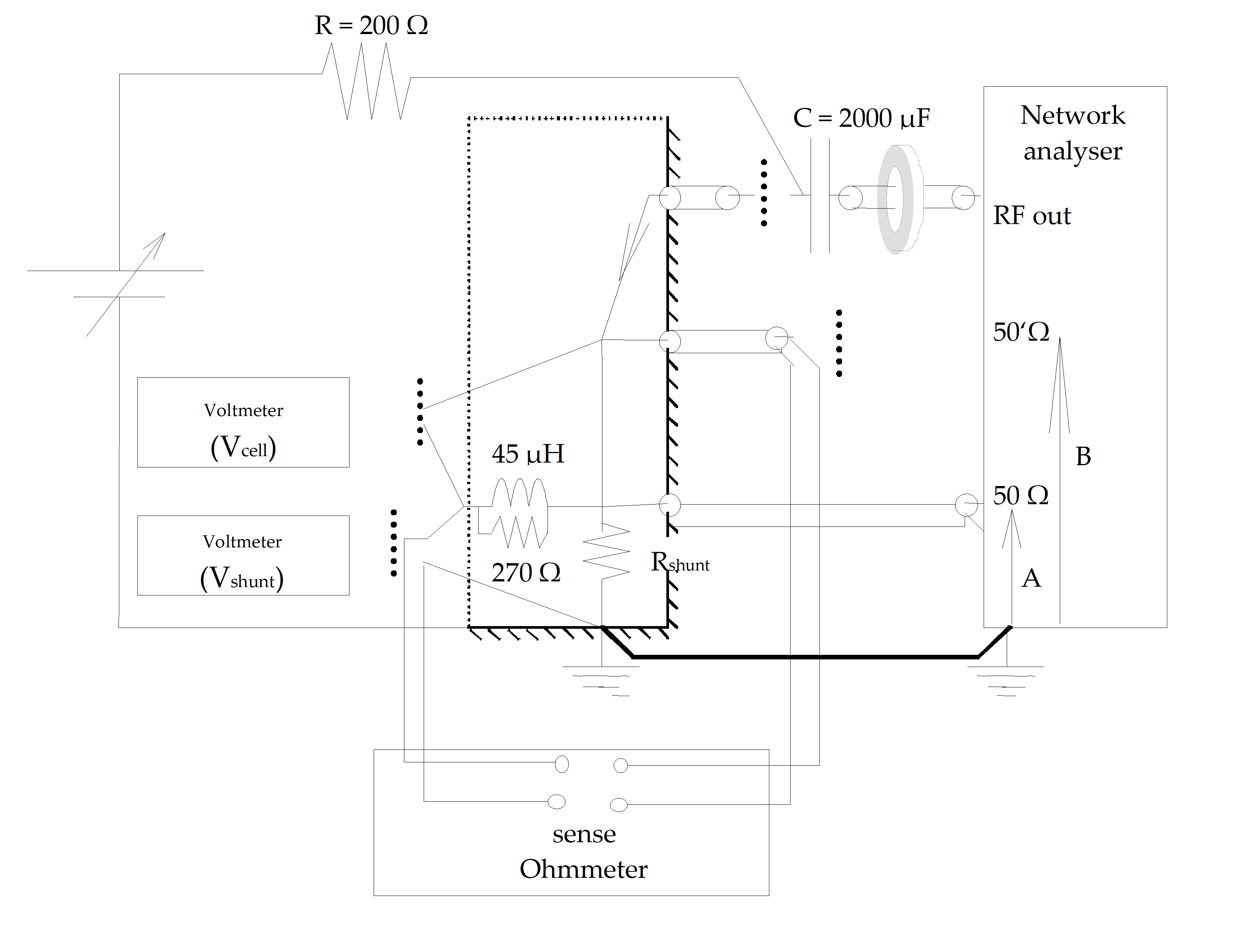 Figure 113: Measurement of the resistance value of the shunt in the measuring conditions (shunt in parallel with the input of the network analyser)
Adjust the injection level of the network analyser as follows:
- Connect the cell in place of the short-circuit and keep the voltage supply at 0 V.
The injection level is selected low enough so as not to generate a variation of the impedance curves when the level changes.
- Begin at 0 dB and lower the signal with 3 dB steps until there is no change at low frequency (variation lower than 0,1 dB).
- Monitor the selected injection level.
Measurement of the cell with the network analyser
The cell should be measured with the network analyser as follows:
- If the measurement is performed at several temperatures in a thermostatic chamber:
- Wait for thermal equilibrium.
- Determine the resistance value of the shunt at each temperature (requirement 11.1.3.2c).
- Determine and record the voltage of the power supply to obtain the bias voltages defined in clause 11.1.1.2 and set the power supply to 0 V at the end.
- Measure the B/A ratios for the chosen bias voltages, as follows. For each bias voltage:
- Adjust the power supply voltage to the determined value.
- Note the cell and the shunt voltages.
- Measure the B/A ratios in the complex form X+j Y; or in the amplitude |B/A| and phase (B/A) from 10 Hz to 10 MHz, and store the data file in the network analyser.
- Note or record the cell voltage change (to detect a temperature increase of the cell).
- Set the power supply voltage to 0 V.
- Record the stored data file.
Measurement analysis
Correction of the measurement with respect to the actual impedance of the shunt (impedance values from the B/A measurements)
For a 1 shunt, the value given by the analyser is the impedance of the cell in series with the 1 resistor, where the cell impedance should be determined using the following calculation:
-
If B/A is given in amplitude |B/A| and phase (B/A), the cell impedance is: Equation Zcell = Rshunt measured

-
If B/A is given in the complex form X+j Y Equation Zcell = Rshunt measured [ 1 +X2 + Y2 – 2X]1/2
Modelling
Calculation of the items of the equivalent network using the impedance values
The small signal electrical model parameters (Figure 114) should be calculated for each bias voltage Vcell,i and bias current Icell,i with respect to the frequency, as follows:

 Figure 114: Small signal electrical schema biased with a DC voltage associated impedance
- Minimize the relative error of the theoretical impedance Ztheo(Ls,Rs,Cp,Rp,) with the measured values (regression by least square method).
As the Nf impedance measurements
![]() are associated to the frequencies
are associated to the frequencies
![]() the function to minimize is
the function to minimize is
![]() which is a function of Ls, Rs, Cp and Rp.
which is a function of Ls, Rs, Cp and Rp.
- Calculate each parameter Rp, Cp, Ls and Rs by successive iterative optimization, one after the other, using the following initial parameters: Rp0 = Z(fMIN),
Cp0 = 1/ (2 fMIN Z(fMIN)),
Ls0 = Z(fMAX) /(2 fMAX),
Rs0 = minimum value of Z(f).
Determination of the capacitance model
From the capacitance measurements at several bias voltages, the following parameters of the model of capacitance should be determined with respect to the cell junction voltage and temperatures:
- C0 (capacitance at 0 V),
- C1 (diffusion parameter), and
- (voltage barrier at measurement temperature), Provision 11.1.4.2.2a should be determined as follows:
- Use the capacitance model based on the following expression:
 where
where
![]() T = measurement temperature
T = measurement temperature
k = 1,38 10-23 J/K
q = 1,602 10-19 C
For measurement in darkness and low currents, the cell voltage Vi and the junction voltage vi are the same (the error is 4 mV for a bias current of 200 mA and a cell serial resistance of 20 m).
- Minimize the relative error between the theoretical capacitance C(C0, , C1, v) and the previously calculated capacitances (regression by least square method).
As the Np impedance measurements
![]() are associated to the voltages
are associated to the voltages
![]() the function to minimize is
the function to minimize is
![]() ,
,
which is the function of C0, and C1.
Calculate each parameter C0, C1 and by successive iterative optimization one after the other, where the initial parameters are as follows:
Equation C0 = C(V1)
![]() Equation - 1, 5 VNp
Equation - 1, 5 VNp
Measurement of the capacitance of a multi-junction cell
The cell capacitance measurement method cannot be directly applied to multi-junction solar cells because it assumes that the photo-currents of each junction of the cell were perfectly matched.
For real cells, this matching is not realized and the voltage profile through the different junctions of the cell is different when the cell is illuminated and when it is in darkness. The measurement in darkness enables the order of magnitude of the capacitance to be evaluated.
In order to obtain a higher precision, these measurements are added to measurements under illumination with the right spectral irradiance.
- 1 Some measurements have been performed and the capacitance has been observed to be higher than the values measured in darkness, even at low bias voltage. This is under experimentation and currently there is not a lot of information available.
- 2 This is the fundamental difference between single junction and multi-junction cells: measurements done in darkness are sufficient to characterize the dynamic behaviour of single junction cells in darkness and under illumination.
- 3 Measurements done in darkness are not sufficient to characterize the dynamic behaviour of multi-junction cells under illumination.
Time domain capacitance measurement
Overview
Introduction
This method is intended to be used for the measurement of the capacitance of SCAs and qualification coupons that are part of power subsystems that use sequential switching shunt regulators.
Description
This clause describes a method for measuring the dynamic properties of a solar cell or qualification coupon, using the time domain method while operating in the current region (to the left of the maximum power point on the curve).
The capacitance of the solar cell or qualification coupon, when switching between two different voltage operational points with the assumptions that
the capacitance is constant between the two points, and
the current is constant in the two points,
is obtained with the expression:
![]() Equation ,
Equation ,
where
I is the measured current at the two points;
t is the time increment;
V is the voltage increment.
The measurements are performed at 1 S.C (AM0) illumination and at constant temperature.
The capacitance that is derived from the short-circuit current point and the operational voltage of the solar cell or qualification coupon is used to derive the requirements for the design of sequential switching shunt regulators specified in ECSS-E-ST-20.
Measurement procedure
Measurement equipment set-up
The time domain capacitance measurement test set-up, should comprise the following test equipment:
- A continuous or pulsed solar simulator according to the requirements specified in clause 10.
- A solar array capacity tester which supplies a synchronizable fast switch to perform a controlled short-circuit release at the open circuit condition of the qualification coupon or SCA under test.
- A digital-analogue oscilloscope to capture the voltage-current transient during the short-circuit release at the open circuit condition.
- A twisted harness of short length to reduce the parasitic inductance of the harness from the test specimen to the capacity tester.
The voltage should be measured at the test specimen terminals.
For qualification coupons with multiple strings, each particular string voltage should be measured not including the string blocking diode (see requirement 5.5.1.3.3f).
External parallel capacitors to derive the capacitance of the qualification coupon or SCA should not be used because this parameter depends on the rate of change of the transient.
Calibration of the measurement equipment
The continuous or pulsed solar simulator should be calibrated according to the requirements specified in clause 10.2.
Performance measurement
The short-circuit release at the open circuit condition of the SCA or qualification coupon should be performed under the illumination conditions specified in clause 11.2.2.2 and at constant temperature.
The voltage curve vs time and the current curve vs time of the test specimen should be recorded during the release.
Data processing
Since the voltage of the test specimen at the moment of the short-circuit release is difficult to measure (due to the high frequency oscillations created by the parasitic harness inductance), one of the following two methods should be used to determine the voltage:
mathematical analysis to find a curve without oscillation that fits the voltage curve measured;
calculation of the intersection of two voltage curves.
Example of two voltage curves that can be used for this purpose are the first voltage curve at the test specimen terminals and the second voltage curve at the capacity tester terminal (+) and test specimen terminal (-).
The voltage determined in requirement 11.2.2.4a should be used to calculate the capacitance according to the expression and conditions specified in clause 11.2.1.2.
ANNEX(normative)Source control drawing for photovoltaic assembly (SCDPVA) DRD
DRD identification
Requirement identification and source document
This DRD is called from ECSS-E-ST-20-08, requirement 5.2b.
Purpose and objective
The source control drawing for photovoltaic assembly (SCD-PVA) contains the specific project dependent requirements, and together with this Standard, which contains the general requirements, constitutes the whole set of requirements for the qualification and acceptance of photovoltaic assemblies.
The SCD-PVA can be produced as a standalone document or as part of a system-level specification document.
The information on traceability to high level requirements can be included in the SCD-PVA itself or in the requirements traceability in the design justification file (DJF, see ECSS-E-ST-10). In either case a cross reference is made.
The SCD-PVA is a major input to the qualification plan.
Expected response
Scope and content
Introduction
The SCD-PVA shall contain a description of the purpose, objective, content and the reasons prompting its preparation.
Applicable and reference documents
The SCD-PVA shall list the applicable and reference documents to support the generation of the document.
Terms and definitions, abbreviated terms and symbols
The SCD-PVA shall include any additional definition, abbreviation or symbol used.
Deviations from ECSS-E-ST-20-08
In conformance with clause 5.2, the SCD-PVA shall include the description and justification for any deviation in the in-process, acceptance and qualification tests.
Qualification test coupons
In conformance with clause 5.5.1.3.3, the SCD-PVA shall include the following:
- In conformance with clause 5.5.1.3.3, the SCD-PVA shall include the front and rear side drawings of each qualification coupons with physical dimensions and including tolerances.
- In conformance with clause 5.5.1.3.3, the SCD-PVA shall include the number of repaired cells to be included on each qualification coupon. In-process tests
Mass measurement
The SCD-PVA shall state the maximum value of the mass of the coupon, in g, obtained from the mass measurement specified in clause 5.4.3.2.
Wet insulation
In conformance with clause 5.4.3.3, the SCD-PVA shall state:
- The test voltage, in V.
- The fluid to use.
- The minimum value for the wet insulation, in M.
- 1 The fluid used is normally ethyl or isopropyl.
- 2 A usual value for the wet insulation is 100 M.
Adherence to substrate
In conformance with clause 5.4.3.4, the SCD-PVA shall state the minimum flatwise tensile strength, in N.
In-process visual inspection
In conformance with clause 5.4.3.5, the SCD-PVA shall state the visual inspection procedure.
In-process continuity
In conformance with clause 5.4.3.6, the SCD-PVA shall state the maximum value of the resistance, in .
Qualification tests
Fatigue thermal cycling
In conformance with clause 5.5.1.3, the SCD-PVA shall state the following:
- The following test conditions:
- the number of cycles to perform;
- the temperature limits, in C.
- For the acceptance criteria:
- the maximum variation of IOP, in %,;
- the minimum insulation, in M.
Humidity
In conformance with clause 5.5.1.4, the SCD-PVA shall state:
- The chemical contents (type and % in the mist) of the humid environment when there are specific requirements on the contents of the environment.
- For the acceptance criteria:
- the maximum variation of IOP, in %,;
- the minimum insulation, in M.
Erosion of materials
In conformance with clause 5.5.1.6, the SCD-PVA shall state the test sequence, test definitions and requirements for the erosion of materials test.
EMC
In conformance with clause 5.5.1.7, the SCD-PVA shall state the test sequence, test definitions and requirements for the EMC test.
Definition of tests and checks
Add-on mass
In conformance with clause 5.5.3.1, the SCD-PVA shall state the maximum add-on mass of the coupon, in g, obtained from a mass measurement.
Full visual inspection
The SCD-PVA shall state:
- The maximum number of cell cracks on the coupons (in conformance with requirement 5.5.3.2.8a.1).
- The maximum number of gridlines that a cell crack can cross (in conformance with requirement 5.5.3.2.8a.2).
- The inspection criteria for solar cells on substrates (in conformance with clause 5.5.3.2.5). Electrical health
For electrical continuity check, in conformance with clause 5.5.3.3.2, the SCD-PVA shall state the following conditions for checking the continuity of the strings:
- current to be applied, in A, or voltage to be measured, in V.
- specified illumination to performed the measurement.
For insulation resistance, the SCD-PVA shall state the minimum insulation resistance, in M, at a test voltage specified in V, for the configurations specified in clause 5.5.3.3.3.
For grounding spot resistance, in conformance with clause 5.5.3.3.4, the SCD-PVA shall state: - The maximum value, in , of the resistance of bleed resistor lead (+) to substrate (-).
- The maximum value, in , of the grounding spots (+) to substrate (-).
For bleed resistor test, in conformance with clause 5.5.3.3.5, the SCD-PVA shall state the range of values, in k, of the bleed resistor.
For blocking diode test, in conformance with clause 5.5.3.3.6, the SCD-PVA shall state: - The IFORWARD in A, and the VREVERSE in V, of the blocking diode.
- The values for VFORWARD, in V, and IREVERSE, in A, to be obtained from the test. For shunt diode, in conformance with clause 5.5.3.3.7, the SCD-PVA shall state:
- The IFORWARD, in A, to be used, and the maximum drop of forward voltage, in V, per cell, to be obtained from the test.
- The test method to be used.
- The maximum temperature, specified in C. For thermal sensor test, in conformance with clause 5.5.3.3.8, the SCD-PVA shall state:
- The resistance of the thermal sensor as a function of the temperature.
- The range of resistance to be obtained from the test, in .
A reference to a calibration table, included in the SCD, can be used.
For resistance measurements, in conformance with clause 5.5.3.3.9, the SCD-PVA shall state the maximum value of the resistance, in , between the (+)/(+) and (-)/(-) ends of the harness.
Electrical performance
In conformance with clause 5.5.3.4.2, the SCD-PVA shall state the following values, together with their inaccuracies, recalculated to 25 C, for 1 S.C. (AM0) (as defined in clause 10), providing the test voltage VOP range (specified in V), and the temperature range (specified in C):
- the nominal value of the IOP,MIN, in A;
- the nominal value of VP,MAX., in V;
- the nominal value of VOC, in V;
- the nominal value of IP,MAX, in A;
- the nominal value of ISC, in A. Capacitance
In conformance with clause 5.5.3.5, the SCD-PVA shall state a procedure to measure the capacitance, including the test temperature (average operational temperature).
Bake-out
In conformance with clause 5.5.3.6, the SCD-PVA shall state: the test conditions, as a combination of time and temperature.
Acceptance thermal cycling test
In conformance with clause 5.5.3.7, the SCD-PVA shall state:
- The following test conditions for the tests specified in clause 5.5.3.7:
- The number of cycles to perform.
- The temperature limits, in C.
- For the acceptance criteria:
- The maximum increment of IOP, in %.
- The minimum insulation, in M.
Reflectance
In conformance with clause 5.5.3.8, the SCD-PVA shall state the maximum reflectance change, in %, for the following wavelength bands:
- 300 nm;
- 300 nm < < 900 nm;
- 900 nm< < 1 800 nm. Transmission
In conformance with clause 5.5.3.9, the SCD-PVA shall state the acceptance criteria for the change in transmission due to contamination in the band of 280 nm < < 2 500 nm.
X-ray
In conformance with clause 5.5.3.9, the SCD-PVA shall state the acceptance criteria, for the integrity of:
- busbars,
- wire collection strips, and
- diode boards. Substrate integrity
In conformance with clause 5.5.3.10, the SCD-PVA shall state:
- The test method, either airscan, or C-scan, or destructive test, for the integrity of the skin to honeycomb.
- The acceptance criteria. Vacuum thermal cycling
In conformance with clause 5.5.3.11, the SCD-PVA shall state the maximum acceptable degradation, as follows:
- The maximum increment for IOP, in %.
- The minimum insulation, in M .
Special remarks
None.
ANNEX(normative)Source control drawing for solar cell assembly (SCDSCA) DRD
DRD identification
Requirement identification and source document
This DRD is called from ECSS-E-ST-20-08, requirement 6.1.2b.
Purpose and objective
The source control drawing for solar cell assembly (SCD-SCA) contains the specific project dependent requirements, and together with this Standard, which contains the general requirements, constitutes the whole set of requirements for the qualification and acceptance of solar cell assemblies.
The SCD-SCA can be produced as a standalone document or as part of a system-level specification document.
The information on traceability to high level requirements can be included in the SCD-SCA itself or in the requirements traceability in the design justification file (DJF, see ECSS-E-ST-10). In either case a cross-reference is made.
The SCD-SCA is a major input to the qualification plan.
Expected response
Scope and content
Introduction
The SCD-SCA shall contain a description of the purpose, objective, content and the reason prompting its preparation.
Applicable and reference documents
The SCD-SCA shall list the applicable and reference documents to support the generation of the document.
Terms and definitions, abbreviated terms and symbols
The SCD-SCA shall include any additional definition, abbreviation or symbol used.
Deviations from ECSS-E-ST-20-08
In conformance with clause 6.1.2, the SCD-SCA shall include the justification for any deviation in the in-process, acceptance and qualification tests.
Materials
The SCD-SCA shall include the following solar cell characteristics:
- For silicon solar cells:
- growth technique, base resistivity, and thickness.
- for ARC: materials
- for metal contact materials and thickness
- For GaAs single or multi-junction solar cells:
- for the substrate: type of material and thickness;
- for each sub-cell: materials,.
- for ARC: materials
- for metal contact materials and thickness
- For interconnects:
- materials and dimensions, all metal layers and their thickness.
- joining technique, additional materials (if any) and reference to the procedure
- For coverglass: material, thickness, ARC, and conductive coating.
- For coverglass adhesive, material and outgassing rates and reference to the procedure for process details and cementing conditions.
See ECSS-Q-ST-70-02.
Test methods, conditions and measurements
Dimensions and weight
In conformance with clause 6.4.3.2, the SCD-SCA shall include:
- A figure, showing the physical dimensions of the solar cell assembly, including both, the nominal values and tolerances.
- The average weight (per lot) of solar cell assemblies including the interconnector, in grams. Electrical performance
In conformance with clause 6.4.3.3, the SCD-SCA shall include, the information shown in Table B-1, extended if there are several operational voltages at a solar cell temperature of 25 C, under illumination of 1 S.C (AM0).
Table: Minimum current requirement for solar assemblies (25 C or operating temperature)
|
Sample
|
Irradiation dose
|
Test voltage
|
Current at
|
|
Minimum for individual solar cell assemblies
|
BOL
|
[Insert value]
|
[Insert value]
|
|
EOL
|
[Insert value]
|
[Insert value]
| |
|
Minimum average for solar cell assemblies
|
BOL
|
[Insert value]
|
[Insert value]
|
|
EOL
|
[Insert value]
|
[Insert value]
| |
|
Test temperature: [Insert value]
| |||
|
NOTE: EOL is defined as 1 MeV p electron dose (in conformance with 6.4.3.12) plus photon irradiation and temperature annealing (in conformance with 6.4.3.13).
| |||
Temperature coefficient
In conformance with clause 6.4.3.4, the SCD-SCA shall include the six equidistant solar cell temperatures to which the test is performed.
Spectral response
In conformance with clause 6.4.3.5, the SCD-SCA shall include for multi-junction GaAs solar cells, the number of narrow band interference filters and their wavelength.
Thermo-optical properties
In conformance with clause 6.4.3.6, the SCD-SCA shall include the following:
- The maximum value of the solar absorptance as a percentage of SCAs with tolerances.
- The maximum value of normal emittance as a percentage (%) of SCAs with tolerances. Thermal cycling
In conformance with clause 6.4.3.7, the SCD-SCA shall include the number of cycles to be performed and their extreme temperatures, to simulate the number of eclipses occurring during one year in orbit for LEO missions, and 1000 thermal cycles for GEO missions, or the complete lifetime cycling for interplanetary or other mission types.
Humidity and temperature
In conformance with clause 6.4.3.8, the SCD-SCA shall include the chemical contents (type and % in the mist) to be added to the humid environment, when there are specific requirements on the contents of the environment.
Coating adherence
In case of coverglass with conductive coating, in conformance with clause 6.4.3.9, the SCD-SCA shall specify which of the two standards ISO 9211-4 or ECSS Q-ST-70-13 shall be applied
Interconnector adherence
In conformance with clause 6.4.3.10 the SCD-SCA shall include:
- the value of the pull speed, in mm/min;
- the pull direction
- the value of the separation pull strength of interconnectors, in N. Electron irradiation
In conformance with clause 6.4.3.11, the SCD-SCA shall include:
- for mission specific qualification, the expected dose for the envisaged application, p, at 1MeV, in e- cm2;
- the electron irradiation at transfer orbit dose at 1MeV, in e- cm2, when specified by the mission requirements. Surface conductivity
In conformance with clause 6.4.3.13, the SCD-SCA shall describe:
- The method to perform the surface conductivity test that shall be between the contact dots or an alternative one to be specified here n the SCD-SCA.
- The minimum value, in , and the maximum variation after any test, in , of the cover conductivity before and after qualification tests of SCA of subgroup D (in conformance with Table 61). Solar Cell reverse bias test
In conformance with clause 6.4.3.14 (it is applicable only for SCAs without protection diode or with a protection diode electrically isolated form the cell).the SCD-SCA shall include:
- The reverse I/V characteristics measured under illumination of 1 S.C.;
- The following measurement parameters shall be clearly stated in the SCD-SCA
- power supply limitation
- temperature
- hold time
- maximum reverse bias voltage
- The pass-fail criteria
- the maximum change in the value of reverse current ∆I, in mA from the initial value of the same parameter when measured as delivered. Pass fail criteria shall be specified in the SCD-SCA.
- the maximum absolute value of the reverse current, in mA.
Ultraviolet exposure
In conformance with clause 6.4.3.15, the SCD-SCA shall include the following:
- The operational test temperature, in C.
- The EOL UV loss factor. Capacitance
In conformance with clause 6.4.3.16, the SCD-SCA shall include the test temperature, in C and the capacitance test method as specified either in clause 11.1 or 11.2 of this Standard.
Flatness
In conformance with clause 6.4.3.17, the SCD-SCA shall include the minimum flatness, as a maximum deviation given in mm.
Special remarks
None.
ANNEX(normative)Source control drawing for bare solar cell (SCDBSC) DRD
DRD identification
Requirement identification and source document
This DRD is called from ECSS-E-ST-20-08, requirement 7.1.1.2b.
Purpose and objective
The source control drawing for bare solar cell (SCD-BSC) contains the specific project dependent requirements, and together with this Standard, which contains the general requirements, constitutes the whole set of requirements for the qualification and acceptance of bare solar cells.
The SCD-BSC can be produced as a standalone document or as part of a system-level specification document.
The information on traceability to high level requirements can be included in the SCD-BSC itself or in the requirements traceability in the design justification file (DJF, see ECSS-E-ST-10). In either case a cross-reference is made.
The SCD-BSC is a major input to the qualification plan.
Expected response
Scope and content
Introduction
The SCD-BSC shall contain a description of the purpose, objective, content and the reason prompting its preparation.
Applicable and reference documents
The SCD-BSC shall list the applicable and reference documents to support the generation of the document.
Terms and definitions, abbreviated terms and symbols
The SCD-BSC shall include any additional definition, abbreviation or symbol used.
Deviations from ECSS-E-ST-20-08
In conformance with requirement 7.1.1.2c, the SCD-BSC shall include the justification for any deviation in the in-process, acceptance and qualification tests.
Materials
The SCD-BSC shall include:
- Reference to the procurement specification of the supplier.
- For silicon solar cells, the following characteristics of the cells:
- growth technique;
- doping element;
- orientation;
- main breakage direction;
- base resistivity;
- thickness;
- for ARC: materials;
- for metal contact materials and thickness.
- For single and multi-junction III-V solar cells, the following characteristics of the cells:
- substrate material, orientation and thickness;
- doping element of the substrate;
- substrate resistivity;
- for each sub-cell: materials,
- for ARC: materials;
- for metal contact materials and thickness.
Acceptance tests
Visual inspection.
In conformance with clause 7.5.1.5.4, the SCD-BSC shall list the maximum visible semiconductor length at the corners, in mm.
Dimensions and weight
In conformance with clause 7.5.2, the SCD-BSC shall include:
- The dimensions shown in Figure C-1 to Figure C-3 including tolerances.
- The measurement method used to perform the test.
- The interval of the thickness of the silicon layer, in m, for silicon solar cells.
- The interval of the thickness of the substrate with epi-layers, in m, for III-IV cells.
- The maximum weight, in mg, of the average shipment lot.
 Figure: BSC front side
 Figure: BSC rear side
 Figure: BSC contact
Contact uniformity
In conformance with clause 7.5.10, the SCD-BSC shall include:
- The equipment to measure the contact thickness;
- The maximum and minimum values of the contact thickness in m. Surface finish
In conformance with clause 7.5.11, the SCD-BSC shall include the maximum value of the surface finish (Rz) in m.
Electrical performance
In conformance with clause 7.3.2.2.2, the SCD-BSC shall include the following test conditions:
- the Vtest, in mV;
- the temperature, in C;
- the cells used as reference and their traceability to primary standards. In conformance with clause 7.3.2.2.3 for the pass-fail criteria, the following requirements shall be included:
- the minimum value for Itest, in mA;
- the average value for Itest, in mA;
In conformance with clause 7.3.2.2.4 the SCD-BSC shall include the intervals in mA for electrical grading
Hemispherical reflectance
In conformance with clause 7.5.6.2, the SCD-BSC shall include the interval of reflectance for silicon BSR cells, at 1,5 m, as a percentage (%).
Humidity and temperature
In conformance with clause 7.5.7.2.2, the SCD-BSC shall include the chemical contents (type and % in the mist) to be added to the humid environment when there are specific requirements on the contents of the environment.
Pull
In conformance with clause 7.5.12, the SCD-BSC shall include:
- the interconnection technique parameter;
- the material and dimension of the interconnectors;
- the value of the pull speed in mm/min;
- the value of the ultimate pull strength in N;
- the pull direction (0°, 45° or 90°). Integral diode performance
In conformance with clause 9.4.5.2, the SCD-BSC shall include for cells with protection diode electrically isolated from the cell:
- For the test specified in requirement 9.4.5.2.2b:
- the temperature,
- the forward current,
- the reverse voltage.
- The pass-fail criteria for the test specified in clause 9.4.5.2.3:
- the maximum absolute value of the forward voltage in V;
- the reverse current in mA.
Cell coverglass gain-loss
In conformance with clause 7.5.6.3, the SCD-BSC shall include:
- the agent used to simulate the properties of the adhesive;
- the coverglass used for the test;
- for the test conditions, the temperature, in C;
- for the pass-fail criteria, the maximum ISC, in %. Qualification
Visual inspection
The SCD-BSC shall include the same provisions as in the visual inspection for the acceptance tests (in conformance with clause C.2.1<6.1>).
Dimensions and weight
The SCD-BSC shall include the same provisions as in the dimensions and weight for the acceptance tests (in conformance with clause C.2.1<6.2>).
Electrical performance
In conformance with clause 7.5.3.2, the SCD-BSC shall include the pass-fail values shown in Table C-1, for
- the individual solar cells, and
- the minimum average. Table: Electrical performance pass-fail criteria
|
Parameter
|
BOL
|
Remaining Factors (at 25 C)
| ||
|
EOL([Insert value]) (particles/cm2)a)
|
EOL([Insert value]) (particles/cm2)a)
|
EOL([Insert value]) (particles/cm2)a)
| ||
|
Ratio
|
Ratio
|
Ratio
| ||
|
VOC [mV]
|
[Insert value]
|
[Insert value]
|
[Insert value]
|
[Insert value]
|
|
Isc [mA/cm2]
|
[Insert value]
|
[Insert value]
|
[Insert value]
|
[Insert value]
|
|
Vmax [mV]
|
[Insert value]
|
[Insert value]
|
[Insert value]
|
[Insert value]
|
|
Imax [mA/cm2]
|
[Insert value]
|
[Insert value]
|
[Insert value]
|
[Insert value]
|
|
Pmax [mW/cm2]
|
[Insert value]
|
[Insert value]
|
[Insert value]
|
[Insert value]
|
|
I(Vt) [mA]
|
[Insert value]
|
[Insert value]
|
[Insert value]
|
[Insert value]
|
|
a) particles are electrons or protons after photon irradiation and temperature annealing
| ||||
Spectral response
If the method using narrow band interference filters the SCD-BSC shall include (in conformance with requirement 7.5.5.2b.1(c) for multi-junction GaAs solar cells the number of narrow band interference filters and their wavelength.
Optical properties
Hemispherical reflectance
- The SCD-BSC shall include the same provisions as in the hemispherical reflectance for acceptance tests (in conformance with clause C.2.1<6.6>). Coverglass gain-loss
- The SCD-BSC shall include the same provisions as in the coverglass gain-loss for acceptance tests (in conformance with clause C.2.1<6.10>). Humidity and temperature
The SCD-BSC shall include the same provisions as in the humidity and temperature for acceptance tests (in conformance with clause C.2.1<6.7>.).
Contact uniformity
In conformance with clause 7.5.9, the SCD-BSC shall include
- the equipment to measure the contact thickness;
- the requirements of the interconnection process to uniformity of the contact.
Example: maximum and minimum values of the contact thickness in m.
Surface finish
The SCD-BSC shall include the same provisions as in the surface finish for acceptance tests (in conformance with clause C.2.1<6.4>).
Pull
The SCD-BSC shall include the same provisions as in the pull test for acceptance tests (in conformance with clause C.2.1<6.8>).
Electron irradiation
In conformance with clause 7.5.13.2, the SCD-BSC shall include:
- For general characterization of solar cells, the dosages at 1 MeV, in e- cm-2.
- For mission specific qualification, the expected dose for the envisaged application, p, at 1MeV, in e- cm-2.
- The electron irradiation at transfer orbit dose at 1MeV, in e- cm-2, when specified by the mission requirements. Proton irradiation
In conformance with clause 7.5.14.2, the SCD-BSC shall include:
- The two energies to which cells of subgroup P are irradiated (X1 and X2 in MeV);
- For each of the two energies defined in C.2.1<7.11> a.1, the flux in p+ cm2 s-2. Solar cell reverse bias
In conformance with clause 7.5.16.2, the SCD-BSC shall include
- the parameters of reverse IV characteristics measurement, such as test temperature in °C, hold time in s, current limitation in mA and maximum reverse bias in V
- the pass/fail criteria
Example: maximum allowed difference in Iop before and after test.
Integral diode
In conformance with clause 9.6, the SCD-BSC shall include for cells with integral protection diode electrically isolated from the cell:
- for burn in (in conformance with clause 9.6.5): the junction temperature of the diode at which burn in is to be performed
- for diode characterization the same provisions as in the diode characterization for the acceptance tests (in conformance with clause C.2.1<6.9>)
- for ESD (in conformance with clause 9.6.16.3): the pass fail criteria
- for switching test (in conformance with requirement 9.6.17.2f): the test conditions and pass fail criteria for level 1 and 2
- for life test (in conformance with requirement 9.6.18.2e): the total number of reverse bias and forward bias test steps, and the IREV, IFW and VFW. Thermal cycling
In conformance with clause 7.5.17, the SCD-BSC shall include the number of thermal cycles to be performed before pull test on subgroup A and after humidity and temperature test in subgroup O, and their extreme temperatures.
Active-passive interface evaluation
In conformance with clause 7.5.18, the SCD-BSC shall include:
- The deviation of total energy in the spectral region of 0,8 m to 1,1 m as a percentage, using a non-infrared rich solar simulator.
- The maximum delta in Voc of the cell under both solar simulator conditions (1 S.C. (AM0) and non-infrared rich). Flatness
In conformance with clause 7.5.19, the SCD-BSC shall include:
- The measurement method used to determine the flatness.
- The minimum flatness, as the maximum value of deflection, in mm.
Special remarks
None.
ANNEX(normative)Source control drawing for coverglass(SCDCVG) DRD
DRD identification
Requirement identification and source document
This DRD is called from ECSS-E-ST-20-08, requirement clause 8.3.1.2b.
Purpose and objective
The source control drawing for coverglass (SCD-CVG) contains the specific project dependent requirements, and together with this Standard, which contains the general requirements, constitutes the whole set of requirements for the qualification and acceptance of coverglass.
The SCD-CVG can be produced as a standalone document or as part of a system-level specification document.
The information on traceability to high level requirements can be included in the SCD-CVG itself or in the requirements traceability in the design justification file (DJF, see ECSS-E-ST-10). In either case a cross-reference is made.
The SCD-CVG is a major input to the qualification plan.
Expected response
Scope and content
Introduction
The SCD-CVG shall contain a description of the purpose, objective, content and the reason prompting its preparation.
Applicable and reference documents
The SCD-CVG shall list the applicable and reference documents to support the generation of the document.
Terms and definitions, abbreviated terms and symbols
The SCD-CVG shall include any additional definition, abbreviation or symbol used.
Deviations from ECSS-E-ST-20-08
In conformance with requirement 8.3.1.2c., the SCD-CVG shall include the justification for any deviation in the in-process, acceptance and qualification tests.
Materials
The SCD-CVG shall include the following coverglass materials characteristics:
- Coverglass base material, including doping elements and percentage (%).
- Front surface coatings (including conductive coatings).
- Rear surface coatings. Marking (coating orientation)
In conformance with clause 8.3.3, the SCD-CVG shall include a figure defining the coating orientation method for coverglass front surface coating identification.
This figure can be the same as the one mentioned in clause D.2.1<8.4>.
Acceptance tests
Sample size for acceptance
In conformance with requirement 8.5.1b, the SCD-CVG shall include the sample size for acceptance.
Transmission into air
The SCD-CVG shall include the same provisions as for the transmission into air for qualification tests (in conformance with clause D.2.1<8.3>).
Dimensions, weight and thickness
The SCD-CVG shall include the same provisions as for the mechanical properties for the qualification tests (in conformance with D.2.1<8.5> a1, 2 and 3).
Visual inspection
The SCD-CVG shall include the same provisions as for the visual inspection for qualification tests (in conformance with clause D.2.1<8.1>).
Humidity and temperature HT2
In conformance with clause 8.7.11.2, the SCD-CVG shall state the chemical contents (type and percentage (%) in the mist) of the humid environment when there are specific requirements on the contents of the environment.
Thermal cycling
The SCD-CVG shall include the same provisions as for the thermal cycling for qualification tests (in conformance with clause D.2.1<8>).
Qualification tests
Qualification test samples
In conformance with clause 8.6.2.2, the SCD-CVG shall include the number of the first production batches from which the coverglass qualification set is obtained.
Visual inspection
In conformance with clause 8.7.1.2, the SCD-CVG shall include:
- The maximum dimensions, in mm, of scratches and digs.
- The maximum number of corner chips per coverglass. Transmission into air
Before the test the SCD-CVG shall include the transmission values shown in Table D-1.
After the test the SCD-CVG shall include the transmission values shown in Table D-2.
TableTable D-1: Average transmission into air before test (%)
|
Discrete wavelength (nm)
|
Wavelength range (nm)
| |||||||
|
400
|
450
|
500
|
600
|
300-320
|
400 - 450
|
600 - 800
|
450 - 1 100
|
900 - 1 800
|
|
[Insert value]
|
[Insert value]
|
[Insert value]
|
[Insert value]
|
[Insert value]
|
[Insert value]
|
[Insert value]
|
[Insert value]
|
[Insert value]
|
TableTable D-2: Maximum average deviation of transmission into air after test (%)
|
|
Discrete Wavelength (nm)
|
Wavelength Range (nm)
| |||||||
|
Environmental
|
400
|
450
|
500
|
600
|
300 - 320
|
400 - 450
|
600 - 800
|
450 - 1 100
|
900- 1 800
|
|
Boiling water
|
[insert value]
|
[insert value]
|
[insert value]
|
[insert value]
|
[insert value]
|
[insert value]
|
[insert value]
|
[insert value]
|
[insert value]
|
|
Humidity and temperature HT1
|
[insert value]
|
[insert value]
|
[insert value]
|
[insert value]
|
[insert value]
|
[insert value]
|
[insert value]
|
[insert value]
|
[insert value]
|
|
Thermal cycling
|
[insert value]
|
[insert value]
|
[insert value]
|
[insert value]
|
[insert value]
|
[insert value]
|
[insert value]
|
[insert value]
|
[insert value]
|
|
UV exposure
|
[insert value]
|
[insert value]
|
[insert value]
|
[insert value]
|
[insert value]
|
[insert value]
|
[insert value]
|
[insert value]
|
[insert value]
|
|
Electron irradiation
|
[insert value]
|
[insert value]
|
[insert value]
|
[insert value]
|
[insert value]
|
[insert value]
|
[insert value]
|
[insert value]
|
[insert value]
|
|
Proton irradiation
|
[insert value]
|
[insert value]
|
[insert value]
|
[insert value]
|
[insert value]
|
[insert value]
|
[insert value]
|
[insert value]
|
[insert value]
|
Electro-optical properties
In conformance with clause 8.7.3, the SCD-CVG shall include a figure showing the nominal values and tolerances for the following electro-optical properties:
- bulk resistivity and surface resistivity;
- refractive index. Mechanical properties
In conformance with clause 8.7.4, the SCD-CVG shall include a figure showing the nominal values and tolerances of the following mechanical properties:
- dimensions (A: length, B: width);
- weight (average per shipping lot);
- density
- thickness;
- edge parallelism;
- perpendicularity of sides.
This figure can be the same as in clause D.2.1<8.4>.
Reflectance properties
In conformance with clause 8.7.5, the SCD-CVG shall include a figure showing the nominal values and tolerances of the following reflectance properties:
- reflectance (including wavelength);
- reflectance cut-on;
- reflectance cut-off;
- reflectance bandwidth.
This figure can be the same as in clause D.2.1<8.4>.
Normal emittance
In conformance with clause 8.7.6, the SCD-CVG shall include the minimum value of the normal emittance, as a percentage (%) and the equipment used to measure the normal emittance.
Surface resistivity
In conformance with clause 8.7.7, the SCD-CVG shall include the minimum value of the surface resistivity, in /cm2, and the equipment used to measure the resistivity.
Flatness or bow
In conformance with clause 8.7.8, the SCD-CVG shall include:
- The minimum value of the flatness or bow, as a maximum deviation, in mm.
- The maximum value of coverglass displacement, from an optically flat surface over a specified distance in mm, for localized flatness deformations, in mm. Transmission into adhesive
In conformance with clause 8.7.9, the SCD-CVG shall include:
- The values as shown in Table D-1.
- The Fresnel’s equation used for the correction of the transmission for reflectance losses including all parameters. HT1 humidity and temperature
In conformance with clause 8.7.11.1, the SCD-CVG shall state the chemical contents (type and percentage (%) in the mist) of the humid environment when there are specific requirements on the contents of the environment.
Electron irradiation
In conformance with clause 8.7.13.2, the SCD-CVG shall state the value of the nominal dose of the electron irradiation, in e- cm-2, and maximum rate, in e- cm-2 s-1.
Proton irradiation
In conformance with clause 8.7.14.2, the SCD-CVG shall state the value of the high and low energy dose of the proton irradiation in p+ cm-2 and maximum flux, in p+ cm-2 s-1.
Breaking strength
In conformance with clause 8.7.15, the SCD-CVG shall state the method to be used to test for the breaking strength and the limits of the breaking strength, in N.
Thermal cycling
In conformance with clause 8.7.16, the SCD-CVG shall state the number of thermal cycles to be performed before contact adhesion and their extreme temperatures.
Special remarks
None.
ANNEX(normative)Source control drawing for External Protection Diodes (SCDEPD) DRD
DRD identification
Requirement identification and source document
This DRD is called from ECSS-E-ST-20-08, requirement 9.2.1.2.2b.
Purpose and objective
The source control drawing for external protection diodes (SCD-EPD) contains the specific project dependent requirements, and together with this Standard, which contains the general requirements, constitutes the whole set of requirements for the qualification and acceptance of external protection diodes.
The SCD-EPD can be produced as a standalone document or as part of a system-level specification document.
The information on traceability to high level requirements can be included in the SCD-EPD itself or in the requirements traceability in the design justification file (DJF, see ECSS-E-ST-10). In either case a cross-reference is made.
The SCD-EPD is a major input to the qualification plan.
Expected response
Scope and content
Introduction
The SCD-EPD shall contain a description of the purpose, objective, content and the reason prompting its preparation.
Applicable and reference documents
The SCD-EPD shall list the applicable and reference documents to support the generation of the document.
Terms and definitions, abbreviated terms and symbols
The SCD-EPD shall include any additional definition, abbreviation or symbol used.
Deviations from ECSS-E-ST-20-08
In conformance with requirement 9.2.1.2.2d, the SCD-EPD shall include the justification for any deviation in the in-process, acceptance and qualification tests.
Materials
The SCD-EPD shall include:
- Reference to the procurement specification of the supplier.
- The following characteristics of the external protection diodes:
- growth technique;
- doping element;
- orientation;
- main breakage direction;
- base resistivity;
- thickness.
Acceptance tests
In conformance with 9.4.1.e, the SCD-EPD shall include the sample size.
For dimensions and weigh, in conformance with clause 9.6.3, the SCD-EPD shall include:
- The lateral dimensions and thickness, including tolerances.
- The contact dimensions, including tolerances.
- The maximum weight, in mg.
For contact thickness, in conformance with clause 9.6.8, the SCD-EPD shall include the maximum and minimum values of the contact thickness in m.
For surface finish, in conformance with clause 9.6.9.3, the SCD-EPD shall include the requirements for the interconnection process.
For humidity and temperature, in conformance with clause 9.6.6., the SCD-EPD shall include the chemical contents (type and % in the mist) to be added to the humid environment when there are specific requirements on the contents of the environment.
For Pull, in conformance with clause 9.6.11, the SCD-EPD shall include: - the interconnection technique parameter;
- the material and dimension of the interconnectors;
- the value of the pull speed in mm/min and direction (0°, 45° or 90°);
- the value of the ultimate pull strength in N. For diode performance, in conformance with clause 9.4.5.2 the SCD-EPD shall include:
- For the test conditions specified in clause 9.4.5.2.2:
- the temperature,
- the forward current level ,
- the reverse voltage level.
- The pass-fail criteria for the test specified in clause 9.4.5.2.3:
- the maximum absolute value of the forward voltage in V;
- the reverse current in mA;
Qualification
Qualification test samples
In conformance with requirement 9.5.4.2b, the SCD-EPD shall include:
- The minimum number of protection diodes from which the qualification lot shall be selected.
- The number of the first production batches from which the qualification lot is obtained. Dimensions and weight
In conformance with clause 9.6.3, the SCD-EPD shall include:
- The lateral dimensions and thickness, including tolerances.
- The contact dimensions, including tolerances.
- The maximum weight, in mg. Diode characteristics
In conformance with clause 9.6.15.2, the SCD-EPD shall include:
- For the test conditions:
- the temperatures,
- the times,
- the forward current level,
- the reverse voltage level.
- The pass-fail criteria for the test specified in clause 9.6.15.3:
- the maximum absolute value of the forward voltage in V;
- the reverse current in mA.
Thermal cycling
In conformance with clause 9.6.4.2, the SCD-EPD shall include the number of thermal cycles and their extreme temperatures.
Burn-in
In conformance with clause 9.6.5.2, the SCD-EPD shall include the temperature of the burning process
Humidity and temperature
In conformance with clause 9.6.6, the SCD-EPD shall include the chemical contents (type and % in the mist) to be added to the humid environment when there are specific requirements on the contents of the environment.
Contact uniformity.
In conformance with clause 9.6.7.3, the SCD-EPD shall include the maximum and minimum values of the contact thickness in m.
Surface finish.
In conformance with clause 9.6.9.3, the SCD-EPD shall include the requirements for the interconnection process.
Pull
In conformance with clause 9.6.11, the SCD-EPD shall include:
- the interconnection technique parameter;
- the material and dimension of the interconnectors;
- the value of the pull speed in mm/min and direction (0°, 45° or 90°);
- the value of the ultimate pull strength in N. Electron irradiation
In conformance with clause 9.6.12.2, the SCD-EPD shall include the expected total dose for the envisaged application, p, at 1MeV, in e- cm-2.
Switching:
In conformance with requirement 9.6.17.2f, the SCD-EPD shall include:
- For level 1: The voltage (VREV), current (IFW), times (T1, T2 and T3) and temperatures.
- For level 2: The voltage (VREV), current (IFW), times (T1, T2 and T3) and temperatures. Life Testing:
In conformance with requirement 9.6.18.2e, the SCD-EPD shall include the total number of test steps in reverse and forward bias mode, VREV, IFW and the maximum allowables IREV and VFW.
In conformance with requirement 9.6.18.2d.1, the SCD-EPD shall include maximum allowable temperature of the diode.
Special remarks
None.
ANNEX(normative)Process identification document (PID) DRD
DRD identification
Requirement identification and source document
This DRD is called from ECSS-E-ST-20-08, requirements 6.2a, 7.2a, 8.4a and 9.3.2a.
Purpose and objective
The purpose of the PID is to have a complete set of documentation defining the traceability of materials, processes and test results of the relevant components or sub-assemblies.
Expected response
Scope and content
The PID shall comprise copies of the definition documents of the SCA, and the manufacturing documents and testing procedures, and include the following:
- in the case of SCAs, a parts list;
- a materials list;
- a list of all manufacturing drawings;
- the production flow chart;
- the specifications for the process used;
- procedures for the inspection performed;
- the overall test programme (including in-process tests and acceptance tests);
- a table of contents with reference number and issue;
- the test matrix for acceptance tests, including requirements and failure criteria;
- the traceability details of the component.
The traceability details are as agreed between customer and supplier.
Special remarks
When a document is company confidential or contains proprietary information, the complete document need not be included.
In the case specified in requirement 11.2.2.4a, a reference to the document shall be included.
ANNEX(normative)Data documentation package (DDP) - DRD
DRD identification
Requirement identification and source document
This DRD is called from ECSS-E-ST-20-08, requirement 5.7a, 6.6a, 7.7a, 8.9a and 9.8a.
Purpose and objective
The DDP is the collection of the data related to the manufacturing, integration and test of the PVA, SCA, BSC, CVG and protection diode, which provides traceability and events records, and is the basis to support the acceptance and qualification of the PVA, SCA, BSC, CVG and protection diode.
Expected response for PVA DDP
Scope and content
The PVA-DDP of coupons for the delivery review board (DRB) shall include, as a minimum, the following items:
- table of contents;
- certificate of conformance;
- shipping documents;
- configuration item data list (CIDL);
- product manufacturing and control file (PMCF);
- parts, materials and processes (PMP) list;
- list of requests for deviations;
- list of requests for waivers;
- list of nonconformances, including copies of nonconformance reports (NCRs) NRB documentation including failure analysis and failed coupon list;
- history record;
- connector mate and de-mate record;
- serialized components list;
- in-process inspection test results, including positioning in the manufacturing flow chart;
- open work or open test;
- replacement or temporary installation record;
- acceptance and qualification test procedures and test reports;
- assembly drawings and circuit diagram;
- notes and comments;
- operation and maintenance manuals and user restrictions;
- minutes of delivery review board (DRB) meetings;
- lower level data documentation packages (DDPs).
Special remarks
None.
Expected response for SCA, BSC, CVG, and Protection diode DDP.
Scope and content
The DDP for SCA, BSC, CVG and protection diode shall consist of cover sheet or sheets, including as a minimum the following:
- reference to the corresponding SCD, including issue and date;
- reference to this Standard, including issue and date;
- component type (for SCDs, BSCs, coverglasses and protection diodes);
- procurement SCA, BSC, CVG and protection diode identification;
- manufacturing SCA, BSC, CVG and protection diode identification;
- number of purchase order or contract;
- deviations from, or additions to, the corresponding SCD and this Standard, if so specified in the order;
- manufacturer’s name and address;
- location of the manufacturing plant;
- signature on behalf of the manufacturer;
- total number of pages of the data package. The DDP for SCA, BSC, CVG and protection diode shall consist of the summary compilation of the final production test data, showing:
- For SCAs, the total number of SCAs submitted to, and the total number rejected after, each of the following tests:
- Visual inspection,
- Control of dimensions,
- Electrical performance measurements,
- Diode performance measurements.
- For BSC, coverglasses and protection diodes, the total number of elements submitted to, and the total number rejected after, each of the acceptance tests. The DDP for SCA, BSC, CVG and protection diode shall consist of the qualification testing data, including:
- For SCAs BSCs, and protection diodes, detailed data of all measurements made in conformance with:
- Table B-1 and Figure 62 (SCAs),
- Annex C (BSCs),
- Annex C (IPD) or Annex E (EPD).
- data of all environmental tests The DDP for SCA, BSC, CVG and protection diode shall consist of failed SCAs, BSCs, CVGs and EPDs list and the corresponding non conformance reports , including:
- The reference number and description of the test or measurement as stated in this Standard or in the corresponding SCD.
- The identification of failed component (for SCDs, BSCs, coverglasses and protection diodes).
- The failed parameter and the failure mode of the component (for SCDs, BSCs, coverglasses and protection diodes).
- A detailed failure analysis report.
The DDP for SCA, BSC, CVG and protection diode shall consist of certificate of compliance.
The DDP for SCA, BSC, CVG and protection diode shall consist of full request of deviations and waivers.
The DDP for SCA, BSC, CVG and protection diode shall consist of qualification test plan.
The DDP for SCA, BSC, CVG and protection diode shall consist of acceptance and qualification test reports.
Special remarks
For identification purposes, each page of the data package shall include the following additional supporting data:
- component type (for SCDs, BSCs, coverglasses and protection diodes);
- manufacturer’s name;
- manufacturing lot identification (for SCDs, BSCs, coverglasses and protection diodes);
- date of establishment of the document;
- page number.
Bibliography
|
ECSS-E-ST-00
|
ECSS system – Description, implementation and general requirements
|
|
ECSS-E-ST-10
|
Space engineering – System engineering
|
|
ECSS-E-ST-20-06
|
Space engineering – Spacecraft charging
|
|
ECSS-Q-ST-10-09
|
Space product assurance — Nonconformance control system
|
|
ECSS-Q-ST-20-07
|
Space product assurance — Quality assurance for test centres
|
|
ECSS-Q-ST-30
|
Space product assurance — Dependability
|
|
ECSS-Q-ST-30-02
|
Space product assurance — Failure modes, effect and criticality analysis (FMECA)
|
|
ECSS-Q-ST-30-11
|
Space product assurance — EEE components — Derating and end–of–life parameter drifts
|
|
ECSS-Q-ST-70
|
Space product assurance — Materials, mechanical parts and processes
|
|
ECSS-Q-ST-70-02
|
Space product assurance — Thermal vacuum outgassing test for the screening of space materials
|
|
ECSS-Q-ST-70-08
|
Space product assurance — Manual soldering of high–reliability electrical connections
|
|
ECSS-Q-ST-70-13
|
Space product assurance — Measurement of the peel and pull–off strength of coating and finishes using pressure–sensitive tapes
|
|
ECSS-Q-ST-70-26
|
Space product assurance — Crimping of high–reliability electrical connections
|
|
ESAPSS-01-202
|
Preservation, storage, handling and transportation of ESA spacecraft hardware
|
|
EN 1939
|
Self adhesive tapes - Determination of peel adhesion properties
|
|
ISO 2859
|
Sampling procedures for inspection by attributes
|
|
ISO 9211-4
|
Optics and optical instruments -- Optical coatings -- Part 4: Specific test methods
|
|
ISO 23038
|
Space systems — Space solar cells — Electron and proton irradiation test methods
|
|
MIL-M-13508
|
Mirror, Front Surfaced Aluminized: for Optical Elements
|
|
MIL-PRF 13830
|
General specification governing the manufacture, assembly and inspection of optical components for fire control instruments
|