
Space product assurance
Derating - EEE components
Foreword
This Standard is one of the series of ECSS Standards intended to be applied together for the management, engineering and product assurance in space projects and applications. ECSS is a cooperative effort of the European Space Agency, national space agencies and European industry associations for the purpose of developing and maintaining common standards. Requirements in this Standard are defined in terms of what shall be accomplished, rather than in terms of how to organize and perform the necessary work. This allows existing organizational structures and methods to be applied where they are effective, and for the structures and methods to evolve as necessary without rewriting the standards.
This Standard has been prepared and maintained under the authority of the Space Components Steering Board (SCSB) in partnership with the European Space Agency (ESA), national space agencies (NSAs) and the European space industry, reviewed by the ECSS Product Assurance Panel and approved by the ECSS Steering Board.
The end-of-life parameter drifts are not covered by this Standard.
Disclaimer
ECSS does not provide any warranty whatsoever, whether expressed, implied, or statutory, including, but not limited to, any warranty of merchantability or fitness for a particular purpose or any warranty that the contents of the item are error-free. In no respect shall ECSS incur any liability for any damages, including, but not limited to, direct, indirect, special, or consequential damages arising out of, resulting from, or in any way connected to the use of this Standard, whether or not based upon warranty, business agreement, tort, or otherwise; whether or not injury was sustained by persons or property or otherwise; and whether or not loss was sustained from, or arose out of, the results of, the item, or any services that may be provided by ECSS.
Published by: ESA Requirements and Standards Division
ESTEC, P.O. Box 299,
2200 AG Noordwijk
The
Copyright: 2011© by the European Space Agency for the members of ECSS
Change log
|
ECSS-Q-60-11A
|
First issue
|
|
ECSS-Q-30-11A
|
Second issue
|
|
ECSS-Q-30-11B
|
Never issued
|
|
ECSS-Q-ST-30-11C
|
Third issue
|
|
ECSS-Q-ST-30-11C Rev 1
|
Third issue Revision 1
|
Introduction
This Standard specifies derating requirements applicable to electronic, electrical and electromechanical components.
Derating is a long standing practice applied to components used on spacecrafts. Benefits of this practice are now proven, but for competitiveness reasons, it becomes necessary to find an optimized reliability. Too high a derating can lead to over-design, over-cost and over-sizing of components, the direct consequence being excess volume and weight. The aim is to obtain reliable and high performance equipment without over-sizing of the components. For this reason and if possible, this Standard provides derating requirements depending on mission duration and mean temperature, taking into account demonstrated limits of component capabilities.
Scope
This Standard applies to all parties involved at all levels in the realization of space segment hardware and its interfaces.
The objective of this Standard is to provide customers with a guaranteed performance and reliability up to the equipment end-of-life. To this end, the following are specified:
Load ratios or limits to reduce stress applied to components;
Application rules and recommendations.
This standard may be tailored for the specific characteristics and constraints of a space project, in accordance with ECSS-S-ST-00.
Normative references
The following normative documents contain provisions which, through reference in this text, constitute provisions of this ECSS Standard. For dated references, subsequent amendments to, or revisions of any of these publications do not apply. However, parties to agreements based on this ECSS Standard are encouraged to investigate the possibility of applying the most recent editions of the normative documents indicated below. For undated references the latest edition of the publication referred to applies.
|
ECSS-S-ST-00-01
|
ECSS system - Glossary of terms
|
|
ECSS-Q-ST-60
|
Space product assurance - Electrical, electronic and electromechanical (EEE) components
|
|
ESCC 2269010
|
Evaluation test programme for monolithic microwave integrated circuits (MMICS)
|
|
ESCC 2265010
|
Evaluation Test Programme for Discrete Microwave Semiconductors
|
Terms, definitions and abbreviated terms
Terms from other standards
For the purpose of this Standard, the terms and definitions from ECSSST0001 apply.
Terms specific to the present standard
ambient temperature
temperature surrounding a component
case temperature
temperature on the component package surface
derating
process of designing a product such that its components operate at a significantly reduced level of stress to increase reliability and to insure useful life and design margins.
hot spot temperature
highest measured or predicted temperature within any component
junction temperature
highest measured or predicted temperature at the junction within a semiconductor or micro-electronic device
Predicted temperature can be taken as Tcase + thermal resistance between junction and case times actual power (Watt) of the device.
load ratio
permissible operating level after derating has been applied; given as a percentage of a parameter rating
operating conditions
parameter stress and environment (temperature, vibration, shock and radiation) in which components are expected to operate
term "performance" deleted
RadPack
package designed to provide some form of radiation protection
rating
maximum parameter value specified and guaranteed by the component manufacturer and component procurement specification
Rating is considered as a limit not to be exceeded during operation and constitutes in most cases the reference for derating.
surge
strong rush or sweep
[Collins dictionary and thesaurus]
transient
brief change in the state of a system
[Collins dictionary and thesaurus]
Abbreviated terms
For the purpose of this Standard, the abbreviated terms from ECSSSST0001 and the following apply:
|
Abbreviation
|
Meaning
|
|
A/D
|
analog to digital
|
|
ASIC
|
application specific integrated circuit
|
|
C
|
capacitance
|
|
DRAM
|
dynamic random access memory
|
|
EEPROM
|
electrical erasable programmable read only memory
|
|
EPROM
|
erasable programmable read only memory
|
|
ESCC
|
European Space Component Coordination
|
|
ESR
|
equivalent series resistance
|
|
f
|
frequency
|
|
FET
|
field effect transistor
|
|
GaAs
|
gallium arsenide
|
|
ISO
|
International Organization for Standardization
|
|
InP
|
indium posphide
|
|
LED
|
light emitting diode
|
|
MOS
|
metal on silicon
|
|
MIL (spec)
|
specification of the US Department of Defense
|
|
MMIC
|
monolithic microwave integrated circuit
|
|
NASA
|
National Aeronautics and Space Administration
|
|
P
|
power
|
|
PROM
|
programmable read only memory
|
|
RadHard
|
radiation hardened
|
|
Ri
|
insulation resistance
|
|
RF
|
radio-frequency
|
|
SEBO
|
single event burn-out
|
|
SEGR
|
single event gate rupture
|
|
Si, SiGe
|
silicon, silicon germanium
|
|
SOA
|
safe operating area
|
|
SRAM
|
static random access memory
|
|
Tj
|
junction temperature
|
|
Tjmax
|
absolute maximum rated junction temperature
|
|
Top
|
operating temperature
|
|
VCE
|
collector-emitter voltage
|
User responsibility
The user of this Standard shall verify that the ordered assurance level of procured components is compatible with the intended application.
Derating
Overview
The term derating refers to the intentional reduction of electrical, thermal and mechanical stresses on components to levels below their specified rating. Derating is a means of extending component life, increasing reliability and enhancing the end-of-life performance of equipment.
Derating participates in the protection of components from unexpected application anomalies and board design variations.
The load ratios or limits given in clause 6 were derived from information available at the time of writing this Standard and do not preclude further derating for specific applications.
This Standard also defines how to handle transients.
Principles of derating
The component parameter strength defines the limits and the performance component technology in the particular application and varies from manufacturer to manufacturer, from type to type, and from lot to lot and can be represented by a statistical distribution. Likewise, component stress can be represented by a statistical distribution. Figure 51 illustrates the strength of a component and the stress applied at a given time, where each characteristic is represented by a probability density function.
A component operates in a reliable way if its parameter strength exceeds the parameter stress. The designer should ensure that the stress applied does not exceed the component parameter strength. This is represented by the intersection (shaded area) in Figure 51. The larger the shaded area, the higher the possibility of failure becomes.
There are two ways, which may be used simultaneously, in which the shaded area can be decreased:
Decrease the stress applied (which moves the stress distribution to the left).
Increase the component parameter strength (by selecting over-sized components) thereby moving the strength distribution to the right.
The goal is to minimize the stress-to-strength ratio of the component. Derating moves the parameter stress distribution to the left while the selection processes applied to the components for space applications contribute to moving the parameter strength distribution to the right. The selection processes also reduce the uncertainty associated with the component parameter strength.
Derating reduces the probability of failure, improves the end-of-life performance of components and provides additional design margins.
Another effect of derating is to provide a safety margin for design. It allows integrating parameter distribution from one component to another, and from one procurement to another.
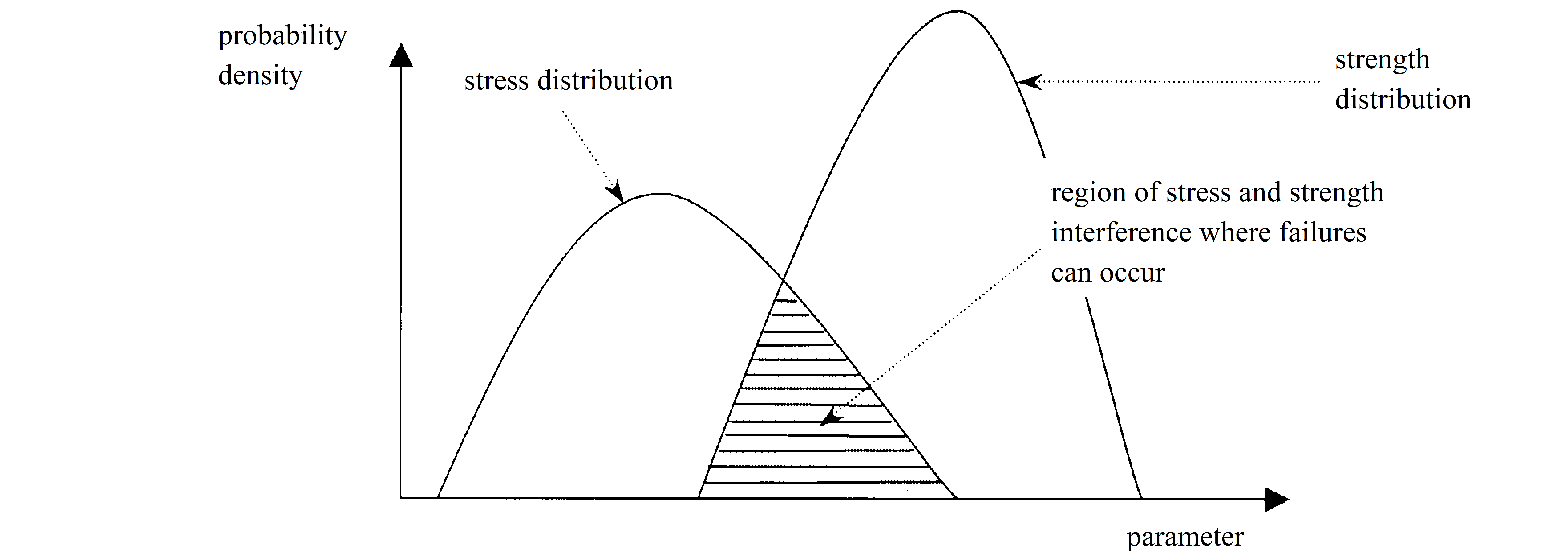 Figure 51: Parameter stress versus strength relationship
Applicability and component selection
Overview
This Standard applies to all components, selected for space applications, that are used for a significant duration. The meaning of “significant duration” is a period that contributes to the component life, for instance, one month is considered to be a significant duration. These requirements apply to screened components procured in accordance with approved space specifications.
This Standard only applies to approved components for which quality was proven after rigorous testing in accordance with ECSS-Q-ST-60.
Derating applies on normal operational conditions, where “normal” is opposed to “fault” and “Operational” indicates all functional modes of the unit.
Derating analysis is performed at the equipment maximum hot acceptance temperature, unless otherwise specified.
Requirements
Derating shall be applied in consideration of temperature limits recommended by the manufacturer.
The derating requirements of this Standard shall not be used as a justification to upgrade the quality level of components.
The derating requirements shall be taken into account at the beginning of the design cycle of an equipment for any consequential design trade-off to be made. Specific attention shall be paid to, for example, breadboards and engineering models where parameter derating was not considered.
Component families and groups excluded in this Standard are due to the lack of experimental data and failure history. For these components, the user shall consult a component design and reliability specialist to apply the requirements of this Standard.
Components may be excluded from this Standard if they are used for short durations of less than one month provided the device ratings are not exceeded; for example, components used in solar generator deployment systems, redundancy commutation and launchers (except in some specific cases, noted family by family). In these cases, the designer shall ensure that the applied stress level does not exceed the component maximum rating.
The derating requirements are not applicable to test conditions (e.g. circuit or equipment level qualification and EMC) for which the maximum ratings shall not be exceeded.
Derating requirements are not applicable to fault conditions, for which the maximum rating shall not be exceeded, with the exception defined in 5.3.2h.
Where components are required to operate in protection mode or in fail-safe mode in order to prevent failure propagation (e.g. short-circuit protection), the components concerned shall meet the derating requirements and application rules when performing the protection or fail-safe function under the worst failure case (i.e. highest stress applied to the components that can last throughout the mission).
Requirements ESCC exceptions
For a particular type or manufacturer, when a specific derating rule is defined in the appendix of the approved ESCC detail specification issued by the ESCC Executive, it shall take precedence over the generic requirement of this standard.
Users shall check for application the actual status of the ESCC Derating exceptions on the following ESCC web site page: ESCC Derating deviations
A list of the ESCC detail specifications applicable at the time of publication and containing deviations to general derating requirements of this standard is available in informative Annex B.
Users shall clearly identify in the Parts Stress Analysis document the list of the ESCC Derating exceptions taken into consideration in their analysis.
Derating parameters
Overview
Derating requirements are provided in clause 6 for each component family.
For each category, the parameters to be derated are identified. The main parameters to be derated are:
junction or case temperature;
power (rating, dissipation);
voltage;
current.
The parameters to be derated depend on component type.
A stress balancing concept offers flexibility between one stress versus another (voltage and temperature). In some cases, e.g. resistors, derating has a direct impact on component performance.
Requirements for transient and surge conditions
For transient or surge conditions, if ratings are provided, the same derating figures as for steady-state equivalent parameters shall be used.
For transient or surge conditions, if ratings are not provided, then it shall be assured that the transient or surge values are below the steady-state specified maximum ratings.
For all periodic signals or transient conditions which are repeated or made incessant, the steady-state derating figures shall apply.
<<deleted>>
As an exception in case clause 5.4.2c is not compatible for specific repeated and incessant transient use conditions, for the parts types and parameters listed, load ratio shall not exceed the steady state derated values +10 % or 80 % of the steady state rated values, which ever is lower:
- Connectors: voltage, current
- Ceramic Capacitors: voltage
- Resistors: current
- Diodes: current
- Transistors_ bipolar , MOSFETs, power FETs: current.
Additional rules and recommendations
Overview
In addition to strict derating requirements, some application rules and recommendations are given in this Standard to achieve the suitable reliability. This additional application rules and recommendations are listed separately in the clauses titled “Additional requirements not related to derating”. This disposition is valid until other adequate ECSS documents can host these additional clauses.
Additional requirements not related to derating
Where radiation sensitive components are identified, it is the user’s responsibility that the chosen component technologies are suitable and that the mitigation factors, such as shielding, meet the customer’s requirement. The electrical derating shall be in accordance with this Standard.
Tables for load ratios or limits
Overview
This clause provides the load ratios or limits.
They are also available on the World Wide Web at the following address:
Abbreviations used in the tables are explained in clause 3.
Annex A contains a complete listing of the family and group codes for parts that are referred to in this Standard.
Annex B contains ESCC exceptions at date of publication of this standard.
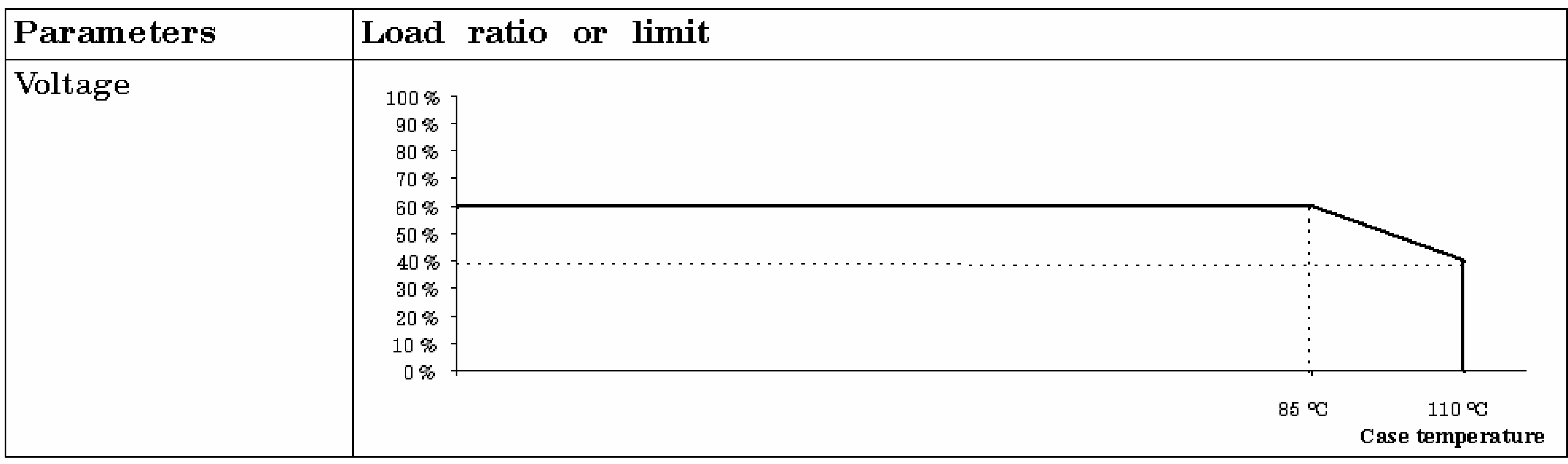
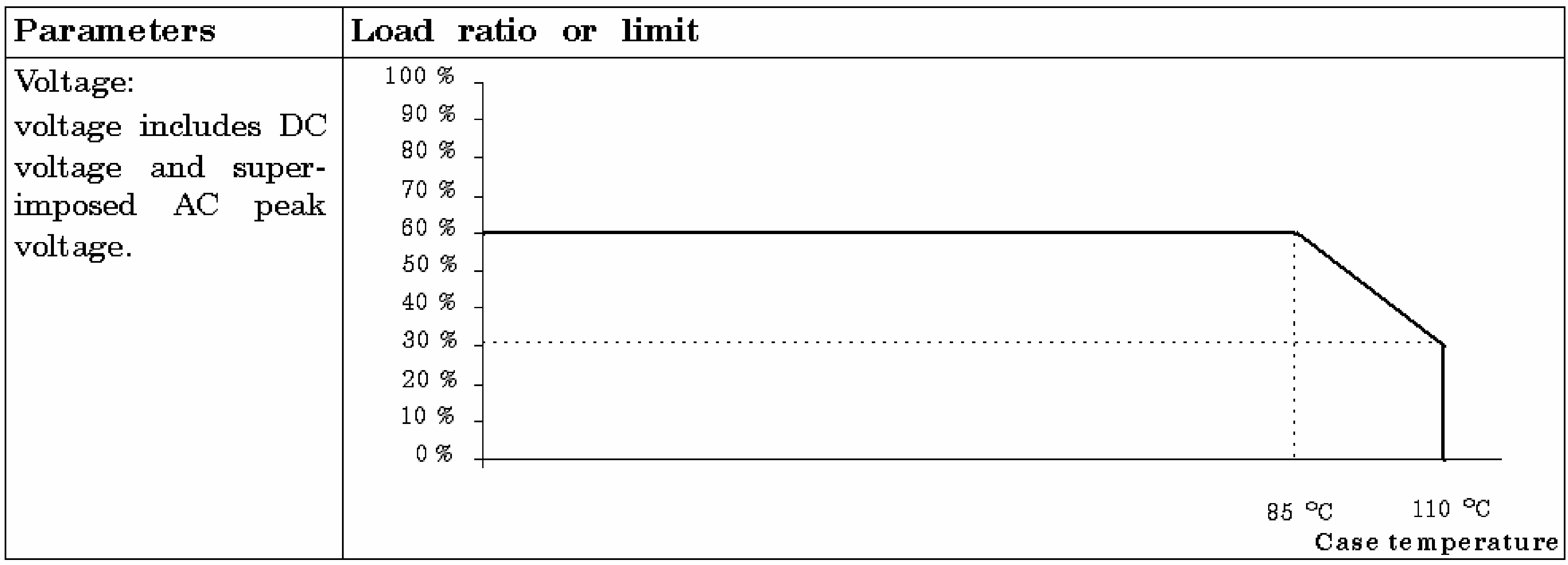
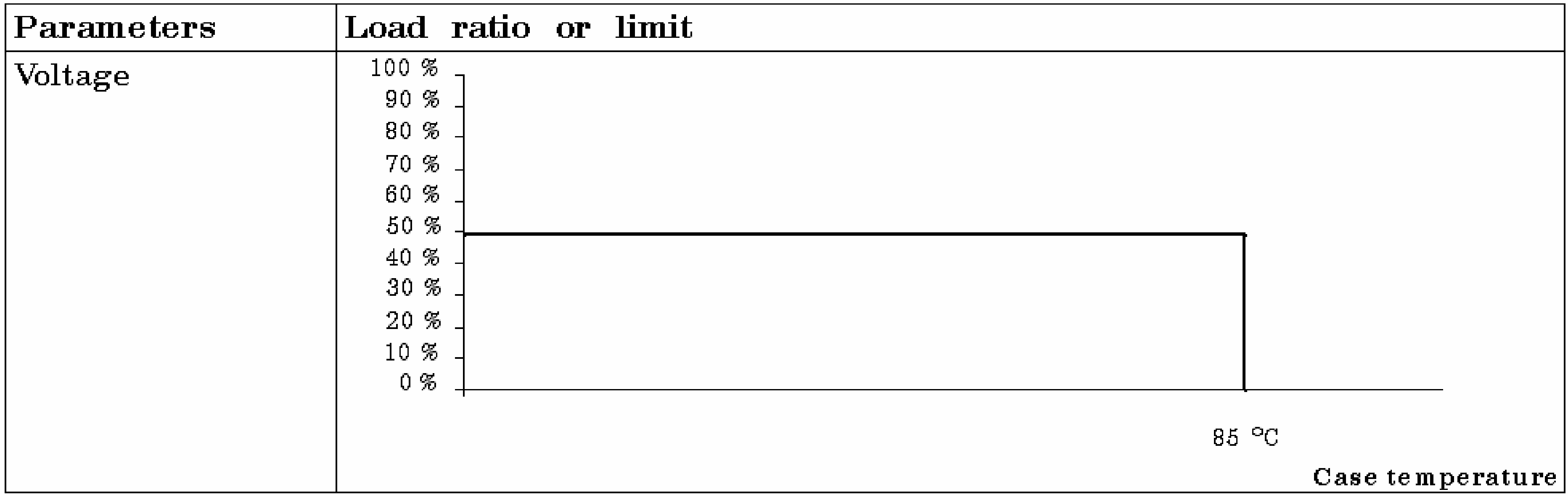
Capacitors: ceramic - family-group code: 01-01 and 01-02
General
The capacitor stress sum value of steady-state voltage, AC voltage shall not exceed the load ratios specified hereunder. For transients refer to clause 5.4.
Multilayer capacitors with a DC voltage rating less than 100 V may be used in low voltage (less than 10 V) continuous applications provided they have been submitted to a low voltage (1,5 V) 85 % humidity at 85 C test or other approved method.
<<deleted>>
Internal heating due to ESR can increase ageing and should be taken into account by applying a margin in temperature. Where ESR is not known at the frequency of a ripple current, an extrapolation of the ESR value and resonance (from manufacturer’s or test data) should be made where possible.
Derating
Parameters of capacitors from family-group code 01-01 and 01-02 shall be derated as per Table 61.
Table 61: Derating of parameters for capacitors family-group code 01-01 and 01-02
Additional requirements not related to derating
The dV/dt rating capability of the capacitors shall be respected.
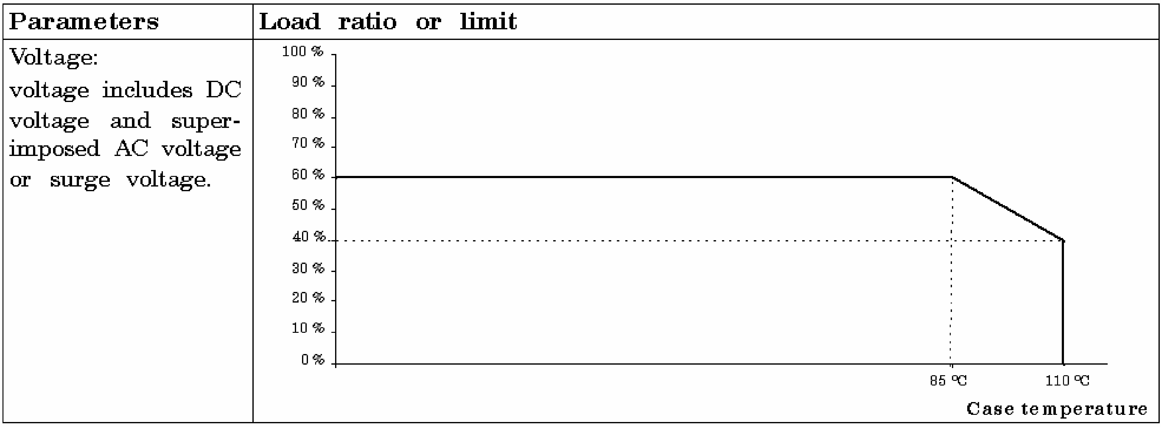
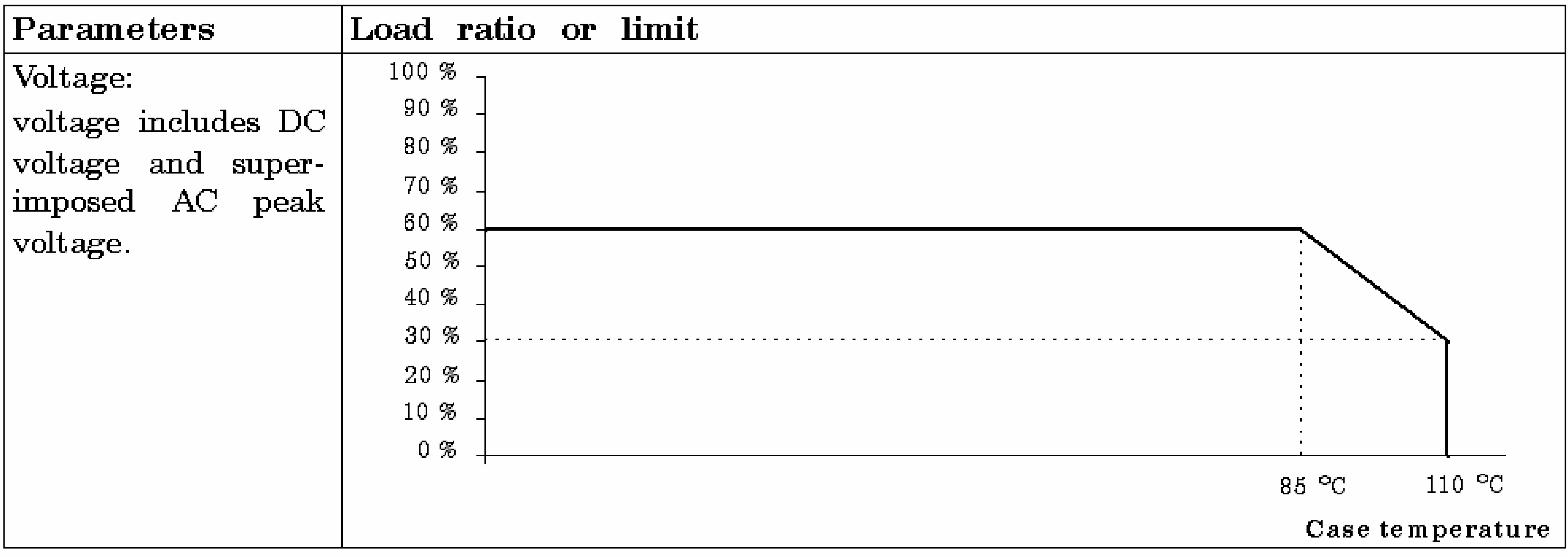
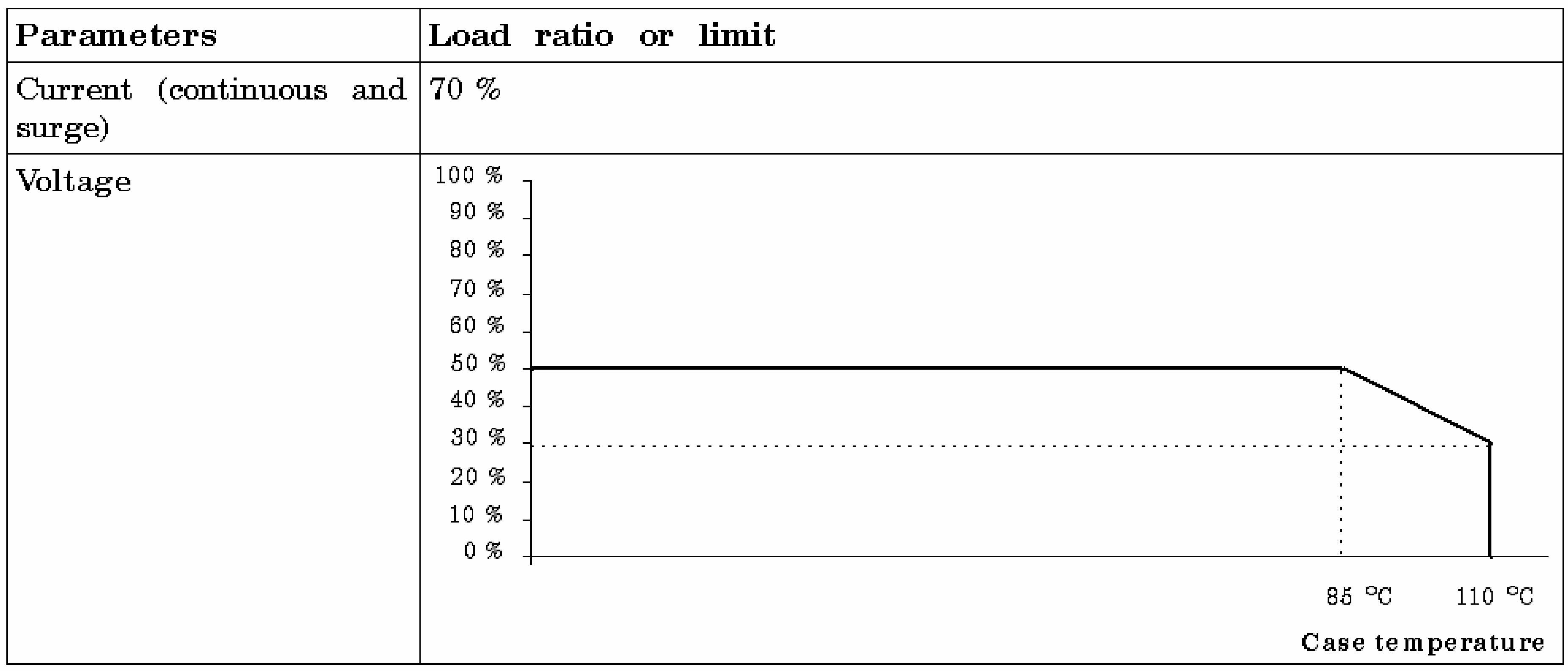
Capacitors: solid tantalum - family-group code: 01-03
General
The capacitor stress sum value of steady-state voltage and AC voltage shall not exceed the load ratio specified hereunder. For transients refer to clause 5.4.
<<deleted - moved to 6.3.3a>>
Surge current shall be derated to 75 % of the Isurge max. Isurge max is defined as Vrated/(ESR+Rs). Vrated is the maximum rated voltage, ESR is the maximum specified value and Rs is the value of series resistance specified in the circuit for surge current testing as defined in the applicable procurement specification.
Reverse voltage shall not exceed 75 % of the manufacturer’s specified maximum value for the reverse voltage.
Ripple power shall never exceed 50 % of the manufacturer’s specified maximum value.
Internal heating due to ESR can increase ageing and should be taken into account by applying a margin in temperature. Where ESR is not known at the frequency of a ripple current, an extrapolation of the ESR value and resonance (from manufacturer’s or test data) should be made where possible.
Derating
Parameters of capacitors from family-group code 01-03 shall be derated as per Table 62.
Table 62: Derating of parameters for capacitors family-group code 01-03
Additional requirements not related to derating
100 % surge current screening shall be applied for all surface mounted capacitors types.
The dV/dt rating capability of the capacitors shall be respected.
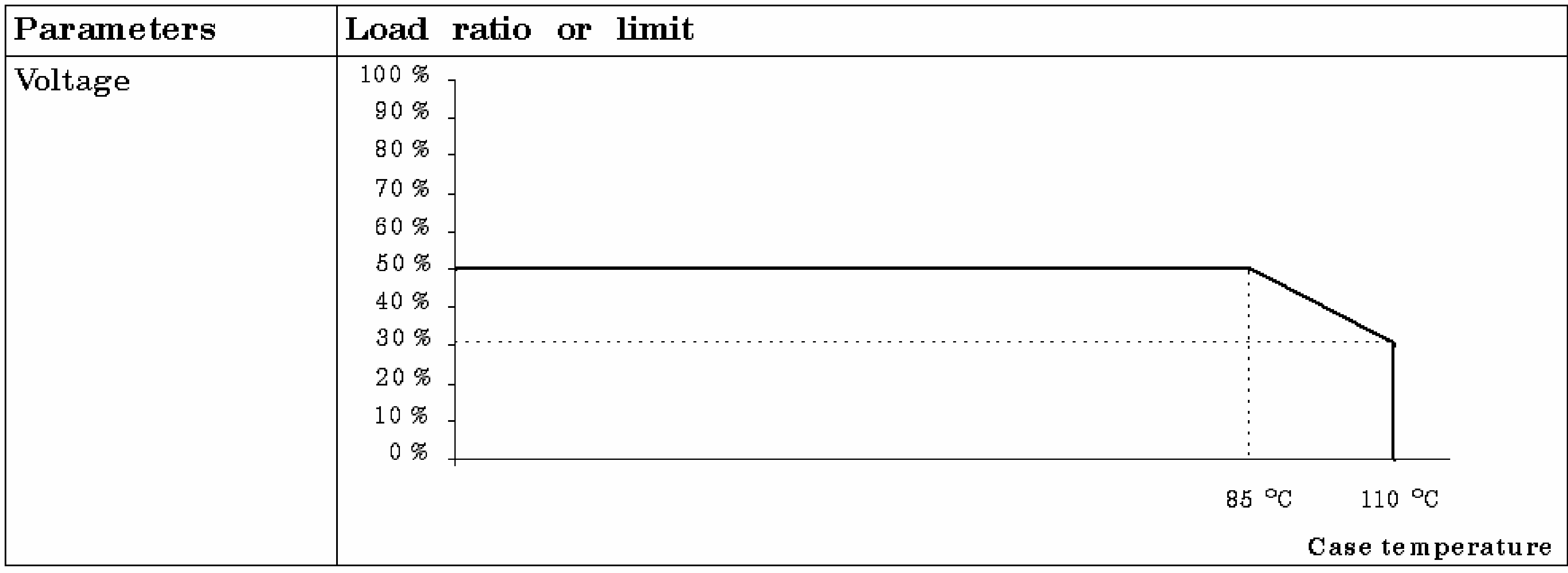
Capacitors: non-solid tantalum - family-group code: 01-04
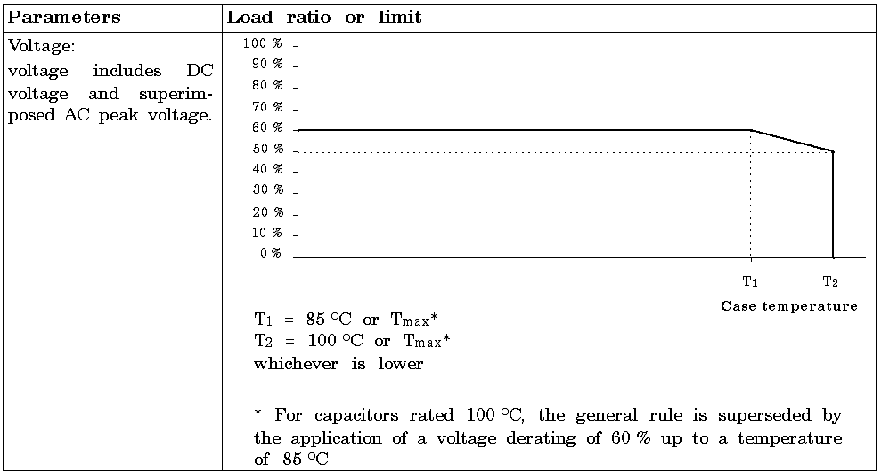
General
Reverse voltage shall not exceed 75 % of the manufacturer’s specified maximum value for the reverse voltage.
Manufacturer’s ratings for ripple power or current shall never be exceeded.
Internal heating due to ESR can increase ageing and should be taken into account by applying a margin in temperature. Where ESR is not known at the frequency of a ripple current, an extrapolation of the ESR value and resonance (from manufacturer’s or test data) should be made where possible.
Derating
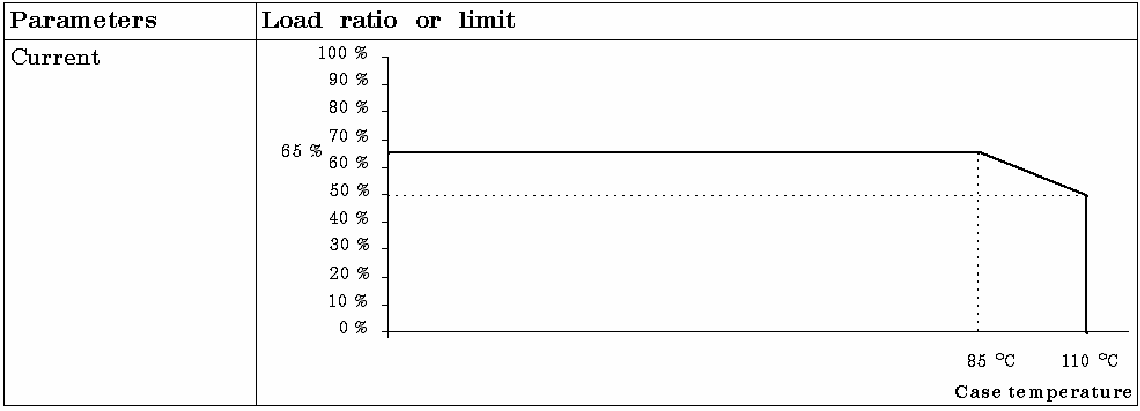
Parameters of capacitors from family-group code 01-04 shall be derated as per Table 63.
Table 63: Derating of parameters for capacitors family-group code
Additional requirements not related to derating
The dV/dt rating capability of the capacitors shall be respected.
Capacitors: Plastic metallized - family-group code: 01-05
General
<<deleted - modified and moved to clause 6.5.3>>
<<deleted>>
Internal heating due to ESR can increase ageing and should be taken into account by applying a margin in temperature. Where ESR is not known at the frequency of a ripple current, an extrapolation of the ESR value and resonance (from manufacturer’s or test data) should be made where possible.
Derating
Parameters of capacitors from family-group code 01-05 shall be derated as per Table 64.
Table 64: Derating of parameters for capacitors family-group code 01-05
Additional requirements not related to derating
Self healing requirements (if applicable): clearing recommendations from manufacturers shall be followed.
The dV/dt rating capability of the capacitors shall be respected.
Capacitors: glass and porcelain - family-group code: 01-06
General
Internal heating due to ESR can increase ageing and should be taken into account by applying a margin in temperature. Where ESR is not known at the frequency of a ripple current, an extrapolation of the ESR value and resonance (from manufacturer’s or test data) should be made where possible.
Derating
Parameters of capacitors from family-group code 01-06 shall be derated as per Table 65.
Table 65: Derating of parameters for capacitors family-group code 01-06
Additional requirements not related to derating
No additional requirement.
Capacitors: mica and reconstituted mica - family-group code: 01-07
General
Internal heating due to ESR can increase ageing and should be taken into account by applying a margin in temperature. Where ESR is not known at the frequency of a ripple current, an extrapolation of the ESR value and resonance (from manufacturer’s or test data) should be made where possible.
Derating
Parameters of capacitors from family-group code 01-07 shall be derated as per Table 66.
Table 66: Derating of parameters for capacitors family-group code 01-07
Additional requirements not related to derating
No additional requirement.
Capacitors: feedthrough - family-group code: 01-10
General
Internal heating due to ESR can increase ageing and should be taken into account by applying a margin in temperature. Where ESR is not known at the frequency of a ripple current, an extrapolation of the ESR value and resonance (from manufacturer’s or test data) should be made where possible.
Derating
Parameters of capacitors from family-group code 01-10 shall be derated as per Table 67.
Table 67: Derating of parameters for capacitors family-group code 01-10
Additional requirements not related to derating
No additional requirement.
Capacitors: semiconductor technology (MOS type) - family-group code: 01-11
General
Internal heating due to ESR can increase ageing and should be taken into account by applying a margin in temperature. Where ESR is not known at the frequency of a ripple current, an extrapolation of the ESR value and resonance (from manufacturer’s or test data) should be made where possible.
Derating
Parameters of capacitors from family-group code 01-11 shall be derated as per Table 68.
Table 68: Derating of parameters for capacitors family-group code 01-11
Additional requirements not related to derating
No additional requirement.
Capacitors: miscellaneous (variable capacitors) - family-group code: 01-99
General
Internal heating due to ESR can increase ageing and should be taken into account by applying a margin in temperature. Where ESR is not known at the frequency of a ripple current, an extrapolation of the ESR value and resonance (from manufacturer’s or test data) should be made where possible.
Derating
Parameters of capacitors from family-group code 01-99 shall be derated as per Table 69.
Table 69: Derating of parameters for capacitors family-group code 01-99
Additional requirements not related to derating
No additional requirement.
Connectors - family-group code: 02-01, 02-02, 02-03, 02-07 and 02-09
General
<<deleted - moved to 6.11.3a>>
<<deleted - moved to 6.11.3b>>
<<deleted - moved to 6.11.3c>>
<<deleted - moved to 6.11.3d>>
Derating
Parameters of connectors from family-group code 02-01, 02-02, 02-03, 02-07 and 02-09 shall be derated as per Table 610.
Table 610: Derating of parameters for connectors family-group code 02-01, 02-02, 02-03, 02-07 and 02-09
|
Parameters
|
Load ratio or limit
|
|
Working voltage
|
50 % of specified voltage at any altitude (pin-to-pin and pintoshell).
|
|
Current
|
50 %
|
|
Hot spot temperature
|
30 C below maximum rated temperature.
|
|
<<deleted>>
|
<<deleted - moved to 6.11.3e>>
|
Additional requirements not related to derating
For power connectors, power and return lines shall be separated by at least one unassigned contact to reduce the short-circuit risk.
Connector savers shall be used during testing of equipment to minimize number of mating and de-mating cycles.
When multi-pin connectors are close to one another, they shall be configured such that mating with a wrong connector is not possible or the contact assignments shall be chosen such that mating with a wrong connector does not cause damage to the unit itself nor to any other element of the system.
The connector and its constituent parts shall be from the same manufacturer.
Maximum mating and de-mating cycles shall be limited to 50 cycles.
Connectors RF - family-group code: 02-05
General
<<deleted - moved to 6.12.3a>>
Derating
Parameters of connectors RF from family-group code 02-05 shall be derated as per Table 611.
Table 611: Derating of parameters for connectors RF family-group code 02-05
|
Parameters
|
Load ratio or limit
|
|
RF power
|
75 %
|
|
Working voltage
|
50 % of specified voltage at any altitude (pin-to-pin and pin-to-shell).
|
|
Hot spot temperature
|
30 C below maximum rated temperature.
|
|
<<deleted>>
|
<<deleted - moved to 6.12.3c>>
|
Additional requirements not related to derating
Connector savers shall be used during testing of equipment to minimize number of mating and demating cycles.
RF power shall be limited such that a 6 dB margin exists before the onset of multipactor.
Maximum mating and de-mating cycles shall be limited to 50 cycles.
Piezo-electric devices: crystal resonator - family-group code: 03-01
General
No general clause.
Derating
Parameters of piezo-electric devices from family-group 03-01 shall be derated as per Table 612.
Table 612: Derating of parameters for piezo-electric devices family-group code 03-01
|
Parameters
|
Load ratio or limit
|
|
Drive level
|
25 % power rated drive level (superseded by manufacturer required minimum drive level if not compatible).
|
Additional requirements not related to derating
No additional requirement.
Diodes - family-group code: 04-01, 04-02, 04-03, 04-04, 04-06, 04-08, 04-10 and 04-14
General
<<deleted - moved to 6.14.3a and 6.14.3b>>
Derating
Diode (signal/switching, rectifier, including Schottky, pin derating table
Parameters of Diode (signal/switching, rectifier including Schottky, pin) shall be derated as per Table 613.
Table 613: Derating of parameters for Diode (signal/switching, rectifier including Schottky, pin)
|
Parameters
|
Load ratio or limit
|
|
Forward current (IF):
|
75%
|
|
Reverse voltage (VR)
|
75 %
|
|
Dissipated power (PD)
|
50 % (only if dissipated power is defined by the manufacturer)
|
|
Junction temperature (Tj )
|
110 C or Tj max - 40 C (whichever is lower).
|
Diode (Zener, reference, transient suppression) derating table
Parameters of Diode (Zener, reference, transient suppression) shall be derated as per Table 614.
Table 614: Derating of parameters for Diode (Zener, reference, transient suppression)
|
Parameters
|
Load ratio or limit
|
|
<<deleted>>
|
<<deleted>>
|
|
Dissipated power (PD)
|
65 %
|
|
Junction temperature (Tj )
|
110 C or Tj max - 40 C (whichever is lower)
|
Additional requirements not related to derating
Some diodes can be radiation sensitive: the issue shall be recorded in the design file and the components selection shall be reviewed and approved as described in ECSS-Q-ST-60.
Where power cycling is critical this should be considered.
The dV/dt rating capability of the diodes shall be respected.
Diodes: RF/microwave - family-group code: 04-05, 04-11 to 04-13, 04-15, 04-16 and 0417
General
<<deleted - moved to 6.15.3a.>>
Derating
Parameters of Diodes from family-group code 04-05, 04-11 to 04-13, 04-15, 04-16 and 0417 shall be derated as per Table 615.
Table 615: Derating of parameters for Diodes family-group code 04-05, 04-11 to 04-13, 04-15, 04-16 and 0417
|
Parameters
|
Load ratio or limit
|
|
Forward current
|
50 %
|
|
Reverse voltage (VR)
|
75 %
|
|
Dissipated power (PD)
|
65 %
|
|
Junction temperature (Tj )
|
110 C or Tj max - 40 C (whichever is lower)
|
|
NOTE 1: Forward current is not applicable to varactors.
| |
Additional requirements not related to derating
Some diodes can be radiation sensitive: the issue shall be recorded in the design file and the components selection shall be reviewed and approved as described in ECSS-Q-ST-60.
Feedthrough filters - family-group code: 05-01
General
No general clause.
Derating
Parameters of Feedthrough filters from family-group code 05-01 shall be derated as per Table 616.
Table 616: Derating of parameters for Feedthrough filters family-group code 05-01
Additional requirements not related to derating
No additional requirement.
Fuses: Cermet (metal film on ceramic) - family-group code: 06-01
General
<<first sentence of requirement deleted - moved to 6.17.3a>>The derating requirements in 6.17.2 (below) are only applicable to Cermet types. The application and the deratings of other fuse technologies shall be justified.
<<deleted - moved to 6.17.3b>>
<<deleted - moved to 6.17.3c>>
Derating
Parameters of Fuses from family-group code 06-01 shall be derated as per Table 617.
Table 617: Derating of parameters for Fuses family-group code 06-01
Additional requirements not related to derating
Fuses shall be avoided whenever possible.
The largest fuse rating compatible with the source capability shall be used.
The power supply shall be capable of delivering three times the specified fuse rated current in order to obtain short fusing times.
Inductors and transformers - family-group code: 07-01 to 07-03 and 14-01
General
<<deleted - moved to 6.18.3a.>>
Derating
Parameters of Inductors and transformers from family-group code: 07-01 to 07-03 and 14-01 shall be derated as per Table 618.
Table 618: Derating of parameters for Inductors and transformers family-group code 07-01 to 07-03 and 14-01
|
Parameters
|
Load ratio or limit
|
Special conditions
|
|
Maximum operating voltage (1)
|
50 % of the applied insulation test voltage (2)
|
(1) Between winding-winding and between windings-case. The maximum operating voltage shall include DC, AC peak or combined.
|
|
Hot spot temperature
|
20 C below maximum rated temperature of any material used.
|
|
Additional requirements not related to derating
For custom-made inductors and transformers, the maximum rated temperature shall be evaluated taking into consideration the temperature characteristics of the materials used.
Unless specified in the procurement specification, the minimum insulation test voltage applied shall be 500 V. For operating voltages greater than 200 V the insulation test voltage is equal to the partial discharge voltage (VPD), defined as the component qualification test level, where the partial discharge activity is detected, and with a test equipment sensitivity of no less than 1 pC.
Integrated circuits: logic - family-group code: 08-10, 08-20, 08-21, 08-29 to 08-42, and 08-80
General
<<deleted - moved to 6.19.3a>>
Derating
Parameters of Integrated circuits from family-group code: 08-10, 08-20, 08-21, 08-29 to 08-42, and 08-80 shall be derated as per Table 619.
Table 619: Derating of parameters for Integrated circuits family-group code: 08-10, 08-20, 08-21, 08-29 to 08-42, and 08-80
|
Parameters
|
Load ratio or limit
|
Special conditions
|
|
Supply voltage (VCC)
|
Manufacturer recommended value ±5 % or 90 % of maximum rating.
|
Supply voltage
|
|
Output current (Iout)
|
80 %
|
|
|
Junction temperature (Tj )
|
110 C or Tj max - 40 C (whichever is lower)
|
<<deleted>>
|
Additional requirements not related to derating
Some devices can be radiation sensitive: this shall be recorded and approved in accordance with ECSS-Q-ST-60.
Integrated circuits: non-volatile memories - family-group code: 08-22, 08-23 and 08-24
General
<<deleted - moved to 6.20.3a>>
Derating
Parameters of Integrated circuits from family-group code: 08-22, 08-23 and 08-24 shall be derated as per Table 620.
Table 620: Derating of parameters for Integrated circuits family-group code: 08-22, 08-23 and 08-24
|
Parameters
|
Load ratio or limit
|
Special conditions
|
|
Supply voltage (VCC)
|
Manufacturer’s recommended value ±5 % or 90 % of maximum rating.
|
Supply voltage
|
|
Output current (Iout)
|
80 %
|
|
|
Maximum junction temperature (Tj max)
|
110 C or Tj max - 40 C (whichever is lower)
|
<<deleted>>
|
|
Endurance and data retention
|
|
Endurance
|
Additional requirements not related to derating
Some devices can be radiation sensitive: this shall be recorded and approved in accordance with ECSS-Q-ST-60.
Integrated circuits: linear - family-group code: 08-50 to 08-60 and 08-69
General
<<deleted - moved to 6.21.1a.>>
<<deleted - moved to 6.21.1b.>>
Derating
Parameters of Integrated circuits from family-group code 08-50 to 08-60 and 08-69 shall be derated as per Table 621.
Table 621: Derating of parameters for Integrated circuits family-group code 08-50 to 08-60 and 08-69
|
Parameters
|
Load ratio or limit
|
Special conditions
|
|
Supply voltage (VCC)
|
90 % of the maximum rated value
|
Supply voltage shall include DC + AC ripple.
|
|
Input voltage (VIN)
|
70 % (or 50 % on the input current) for operational amplifiers.
|
|
|
Output current (Iout)
|
80 %
|
|
|
Transients
|
Shall not exceed the specified maximum ratings.
|
|
|
Maximum junction temperature (Tj max)
|
110 C or Tj max - 40 C, whichever is lower.
|
|
Additional requirements not related to derating
Some linear circuits can be radiation sensitive: the issue shall be recorded in the design file and the components selection shall be reviewed and approved as described in ECSS-Q-ST-60.
Additional margins can be applied for radiation effects.
Integrated circuits: linear converters - family-group code: 08-61 and 08-62
General
<<deleted - moved to6.22.3a.>>
Derating
Parameters of Integrated circuits from family-group code 08-61 and 08-62shall be derated as per Table 622.
Table 622: Derating of parameters for Integrated circuits family-group code 08-61 and 08-62
|
Parameters
|
Load ratio or limit
|
Special conditions
|
|
Junction temperature (Tj )
|
110 C or Tj max - 40 C, whichever is lower.
|
|
|
Supply voltage (VCC)
|
90 %
|
Supply voltage shall include DC + AC ripple.
|
|
Input voltage (VIN)
|
100 % or derated circuit supply voltage, whichever is less.
|
|
|
Output current (Iout)
|
80 % (D/A converters only)
|
|
Additional requirements not related to derating
Some linear circuits can be radiation sensitive: the issue shall be recorded in the design file and the components selection shall be reviewed and approved as described in ECSS-Q-ST-60.
Integrated circuits: MMICs - family-group code: 08-95
General
<<deleted - moved to 6.23.3a.>>
Derating
Each discrete cell (capacitors, resistors, diodes and transistors) constituting analogue custom MMICs shall be derated in accordance with this document’s requirements for the applicable family. For digital cells, apply the derating rules applicable to integrated circuits.
When operational reliability data is available, the compression level shall be derated to 2 dB under the highest compression level showing no drift. MMICs having no compression data shall not be submitted to more than 1 dB of compression.
Additional requirements not related to derating
Some MMICs can be radiation sensitive: the choice of MMICs shall be based on suitability and application. Justification shall be in accordance with ECSS-Q-ST-60 and provided in accordance with this Standard, and at the design reviews
Integrated circuits: miscellaneous - family-group code: 08-99
General
<<deleted - modified and moved to 6.24.2a>>
<< deleted - moved to 6.24.3a>>
Derating
For all ICs not considered in the previous subgroups, the following derating rules shall be followed:
- Manufacturer’s derating values.
- Junction temperature: 110 C or Tj max - 40 C, whichever is lower.
- For the part of the IC similar to logic ICs, apply the derating rules for logic subgroups, for the part similar to linear ICs, apply the derating rules for linear subgroups and so forth.
Additional requirements not related to derating
Some integrated circuits can be radiation sensitive: this shall be recorded and approved in accordance with ECSS-Q-ST-60.
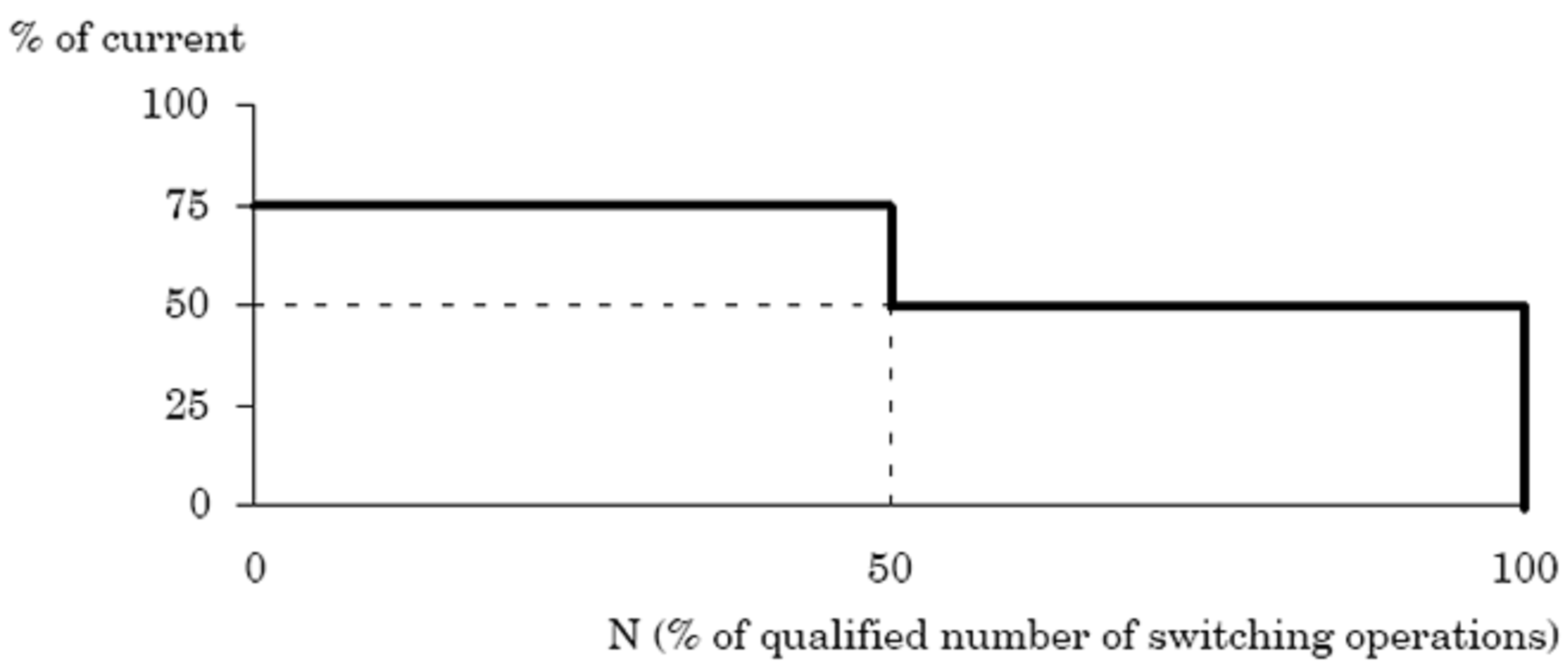
Relays and switches - family-group code: 09-01, 0902 and 16-01
General
The coil supply voltage shall be within the specified voltage range or between the specified rated and the maximum coil voltage. When no minimum coil voltage is provided, the coil voltage shall be between 110 % of the maximum latch or reset or pick-up voltage over the full temperature range and the maximum coil voltage.
Latch or reset voltage are specified for latching device, pick-up voltage is specified for non-latching devices.
The minimum coil pulse duration for latching relays shall be 3 times the latch time (tL) or 40 ms, whichever is greater.
<<deleted - moved to 6.25.3a>>
Rated contact load voltage should not be exceeded since it has a strong impact on the contact current: this shall be recorded and approved in accordance with ECSS-Q-ST-60.
<<deleted - moved to 6.25.3b>>
<<deleted - moved to 6.25.3c.>>
<<deleted - moved to 6.25.3d.>>
Derating
Parameters of Relays and switches from family-group code 09-01, 0902 and 16-01 shall be derated as per Table 623.
Table 623: Derating of parameters for Relays and switches family-group code 09-01, 0902 and 16-01
|
Parameters
|
Load ratio or limit
|
|
Contact current
|
|
|
|
Number of operations less than 100 (including integrating and testing)
|
|
Inductive load
|
50 % of inductive load if specified, or 40 % of resistive load otherwise. If an arc suppressor or snubber system is used, the load factor for resistive load may be applied.
|
|
Motor load
|
50 % of motor load if specified, or 20 % of resistive load otherwise
|
|
Filament load
|
10 % of resistive load.
|
|
Minimum contact current
|
For rated contract current (ICR) 1 A, no limit needs to be considered.
|
|
Surge contact current (ISCR)
|
When the surge duration 10 s, the surge contact current shall not exceed 4 times the rated contact current.
|
Additional requirements not related to derating
Current derating does not apply to contacts that only carry current and do not switch it or to contacts that switch at zero current. In the latter case, the number of operations is limited to the qualified number of operations.
A double throw contact shall not be used to switch a load (movable contact) between a power supply and ground (stationary contacts). This type of configuration may be accepted in the following conditions:
- when switching off the power supply the other stationary contact is not connected to ground, or
- the potential difference between stationary contacts is less than 10 V and the switched current less than 0,1 A.
Paralleled relays shall not be used to increase current switching capabilities of contacts. When relays are paralleled for redundancy, in order to increase the system’s reliability, the sum of the paralleled currents shall not exceed the contact current rating.
Suppression diodes shall not be used inside relays.
Resistors - family-group code: 10-01 to 10-11
General
No general clause.
<<deleted>>
<<deleted - moved as Note to derating tables Table 624 to Table 630>>
<<6.26.1.2 to 6.26.1.7 deleted - modified and moved to 6.26.2.1 to 6.26.2.7>>
<<6.26.1.8 to 6.26.1.10 deleted>>
Derating
<<deleted - moved to 6.26.2.8a including the derating table>>
Metal film precision resistor (type RNC, except RNC 90) derating table
Parameters of Metal film precision resistor (type RNC, except RNC 90) shall be derated as per Table 624.
Table 624: Derating of parameters for Metal film precision resistor (type RNC, except RNC 90)
|
Parameters
|
Load ratio or limit
|
|
Voltage
|
80 %
|
|
rms Power
|
50 % up to 125 C and further decreasing to 0 % at 150 C
|
|
NOTE: The mentioned temperatures cited refer to case temperatures.
| |
Metal film semi-precision resistor (type RLR) derating table
Parameters of Metal film semi-precision resistor (type RLR) shall be derated as per Table 625.
Table 625: Derating of parameters for Metal film semi-precision resistor (type RLR)
|
Parameters
|
Load ratio or limit
|
|
Voltage
|
80 %
|
|
rms Power
|
50 % up to 70 C and further decreasing to 0 % at 125 C
|
|
NOTE: The mentioned temperatures cited refer to case temperatures.
| |
Foil resistor (type RNC 90) derating table
Parameters of Foil resistor (type RNC 90) shall be derated as per Table 626.
Table 626: Derating of parameters for Foil resistor (type RNC 90)
|
Parameters
|
Load ratio or limit
|
|
Voltage
|
80 %
|
|
rms Power
|
50 % up to 70 C and further decreasing to 0 % at 125 C
|
|
NOTE: The mentioned temperatures cited refer to case temperatures.
| |
Wire-wound high precision resistor (type RBR 56) derating table
Parameters of Wire-wound high precision resistor (type RBR 56) shall be derated as per Table 627.
Table 627: Derating of parameters Wire-wound high precision resistor (type RBR 56)
|
Parameters
|
Load ratio or limit
|
|
Voltage
|
80 %
|
|
rms Power (type RBR 56)
|
Wire-wound for all tolerances: 50 % up to 115 C, decreasing to 0 % at 130 C
|
|
NOTE: The mentioned temperatures cited refer to case temperatures.
| |
Wire-wound power resistor (type RWR, RER) derating table
Parameters of Wire-wound power resistor (type RWR, RER) shall be derated as per Table 628.
Table 628: Derating of parameters for Wire-wound power resistor (type RWR, RER)
|
Parameters
|
Load ratio or limit
|
|
Voltage
|
80 %
|
|
rms Power
|
60 % up to 25 C, decreasing to 0 % at 175 C
|
|
NOTE: The mentioned temperatures cited refer to case temperatures.
| |
Chip resistor (RM), network resistor derating table
Parameters of Chip resistor (RM), network resistor shall be derated as per Table 629.
Table 629: Derating of parameters for Chip resistor (RM), network resistor
|
Parameters
|
Load ratio or limit
|
|
Voltage
|
80 %
|
|
rms Power
|
50 % up to 85 C, decreasing to 0 % at 125 C
|
|
NOTE: The mentioned temperatures cited refer to case temperatures.
| |
Carbon composition resistor table
Parameters of Carbon composition resistor shall be derated as per Table 630.
Table 630: Derating of parameters for Carbon composition resistor
|
Parameters
|
Load ratio or limit
|
|
Voltage
|
80 %
|
|
rms Power
|
50 % up to 70 °C, decreasing to 0 % at 100°C
|
|
NOTE: The mentioned temperatures cited refer to case temperatures.
| |
Heaters
Actual rated power shall be specified in the applicable heater design drawing. It shall be determined from the specified heating area (s) in cm2 taking into account the thermal properties of the mounted heater in the application.
Parameters of heaters shall be derated as per Table 631.
Table 631: Derating of parameters for Heaters
|
Parameters
|
Load ratio or limit
|
|
Actual rated power (W)
|
50 %
|
Additional requirements not related to derating
No additional requirement.
Thermistors - family-group code: 11-01 to 11-03
General
No general clause.
Derating
Parameters of Thermistors from family-group code 11-01 to 11-03 shall be derated as per Table 632.
Table 632: Derating of parameters for Thermistors family-group code 11-01 to 11-03
|
Parameters
|
Load ratio or limit
|
|
Power
|
50 % of the maximum power
|
Additional requirements not related to derating
No additional requirement.
Transistors: bipolar - family-group code: 12-01 to 12-04 and 12-09
General
<<deleted - moved to 6.28.3a>>
Derating
Parameters of Transistors from family-group code 12-01 to 12-04 and 12-09 shall be derated as per Table 633.
Table 633: Derating of parameters for Transistors family-group code 12-01 to 12-04 and 12-09
|
Parameters
|
Load ratio or limit
|
|
Collector-emitter voltage (VCE0)
|
75 %
|
|
Collector-base voltage (VCB0)
|
75 %
|
|
Emitter-base voltage (VEB0)
|
75 %
|
|
Collector current (IC max)
|
75 %
|
|
Base current (IB max), if specified
|
75 %
|
|
Power (PD)
|
65 % of maximum power
|
|
Junction temperature (Tj )
|
110 C or Tj max - 40 C (whichever is lower).
|
|
<<Notes deleted and moved to 6.28.3b and 6.28.3c>>
| |
Additional requirements not related to derating
Some transistors can be radiation sensitive: the issue shall be recorded in the design file and the components selection shall be reviewed and approved as described in ECSS-Q-ST-60.
The designer should refer to the SOA
Where power cycling is critical this should be considered
Transistors: FET - family-group code: 12-05 and 12-06
General
<<deleted - moved to 6.29.3a>>
<<deleted - moved to 6.29.3b>>
Derating
Parameters of Transistors from family-group code 12-05 and 12-06 shall be derated as per Table 634.
Table 634: Derating of parameters for Transistors family-group code 12-05 and 12-06
|
Parameters
|
Load ratio or limit
|
|
Drain to source voltage (VDS)
|
80 % of rated,
|
|
Gate to source voltage (VGS)
|
75% of rated,
|
|
Drain current (IDS)
|
75 %
|
|
Power dissipation (PD) max
|
65 % max
|
|
Junction temperature (Tj )
|
110 C or Tj max - 40 C (whichever is lower)
|
Additional requirements not related to derating
Only SEE radiation characterized MOSFETs shall be used in space applications.
Where power cycling is critical this should be considered.
Transistors: RF: bipolar - family-group code: 12-10 and 12-13
General
<<deleted - moved to 6.30.3a.>>
Derating
Parameters of Transistors from family-group code 12-10 and 12-13 shall be derated as per Table 635.
Table 635: Derating of parameters for Transistors family-group code 12-10 and 12-13
|
Parameters
|
Load ratio or limit
|
|
Collector-emitter voltage (VCE)
|
75 %
|
|
Collector-base voltage (VCB)
|
75 %
|
|
Emitter-base voltage (VEB)
|
75 %
|
|
Collector current (IC)
|
75 %
|
|
Base current (IB), if specified
|
75 %
|
|
Power dissipation (PD)
|
65 % or limited by the derating on operating temperature.
|
|
Junction temperature (Tj )
|
110 C or Tj max - 40 C (whichever is lower) for Si and SiGe bipolar transistors.
|
|
NOTE When supported by reliability data, the compression level (including worst case modulation peak compression) is derated to 2 dB under the highest compression level showing no drift. No compression levels exceeding 1 dB are applied to Bipolar transistors without compression data.
| |
Additional requirements not related to derating
Some transistors can be radiation sensitive: the issue shall be recorded in the design file and the components selection shall be reviewed and approved as described in ECSS-Q-ST-60.
Transistors: RF: FET - family-group code: 12-12, 12-14, 12-15(FET) and 12-16(FET)
General
<<deleted - moved to 6.31.3a.>>
Derating
Parameters of Transistors from family-group code 12-12, 12-14, 12-15(FET) and 12-16(FET)shall be derated as per Table 636.
Table 636: Derating of parameters for Transistors family-group code 12-12, 12-14, 12-15(FET) and 12-16(FET)
|
Parameters
|
Load ratio or limit
|
|
Drain to source voltage (VDS)
|
75 %
|
|
Gate to source voltage (VGS)
|
75 %
|
|
Gate to drain voltage (VGD)
|
75 %
|
|
Drain current (IDS)
|
75 %
|
|
Power dissipation (PD)
|
80 % or limited by the derating on operating temperature.
|
|
Junction temperature (Tj )
|
110 C or Tj max - 40 C (whichever is lower) for Si FET transistors.
|
|
NOTE: When supported by reliability data, the compression level (including worst case modulation peak compression) is derated to 2 dB under the highest compression level showing no drift. No compression levels exceeding 1 dB are applied to FETs without compression data.
| |
Additional requirements not related to derating
Some transistors can be radiation sensitive: this issue shall be recorded in the design file and the components selection shall be reviewed and approved as described in ECSS-Q-ST-60.
Wires and cables - family-group code: 13-01 to 13-03
General
No general clause.
Derating
Parameters of Wires and cables from family-group code 13-01 to 13-03 shall be derated as per Table 637.
The derating on current for bundles (IBW) with N wires shall be calculated as IBW = ISW × K, with ISW the derated current for single wire and K as per Table 638.
In case of wires in cold redundancy or wires non used in the same bundle (some with current, others without current) the number of wires to take into account is calculated as follows: N equivalent bundle = N wires with current + 0,5 x N wires without current with IBW which shall not overpass ISW.
Table 637: Derating of parameters for Wires and cables family-group code 13-01 to 13-03
|
Parameters
|
Load ratio or limit
| ||||||||||||||
|
Voltage
|
50 %
| ||||||||||||||
|
Wire size (AWG)
|
32
|
30
|
28
|
26
|
24
|
22
|
20
|
18
|
16
|
14
|
12
|
10
|
8
|
6
|
4
|
|
Maximum current for single wire Cu (Isw) (A) a
|
1,2
|
1,3
|
1,5
|
2,5
|
3,5
|
5
|
7,5
|
10
|
13
|
17
|
25
|
32
|
45
|
60
|
81
|
|
Maximum current for single wire Al (Isw) (A) a
|
|
|
|
|
|
4
|
6
|
8
|
10,4
|
13,6
|
18,4
|
25,6
|
36
|
|
|
|
Wire surface temperature
|
Manufacturer’s maximum rating Tmax -50 C .
| ||||||||||||||
|
a for ambient temperature of 40 °C.
| |||||||||||||||
Table 638: Bundle factor K for calculation of the derated current for each individual wire in bundles of N wires
|
Wires AWG 12 to AWG 32 |
Wires AWG 0 to AWG 10 |
||
|
Number of wires (N) |
K |
Number of wires (N) |
K |
|
1 < N 3 3 < N 7 7 < N 19 19 < N 331 |
1,1 - (0,1 × N) 1,01 - (0,07 × N) 0,81 - [0,15 × ln(N)] 0,59 - [0,076 × ln(N)] |
1 < N 3 3 < N 7 7 < N 52 52 < N 331 |
1,1 - (0,1 × N) 1,01 - (0,07 × N) 0,81 - [0,15 × ln(N)] 0,467 - [0,0632 × ln(N)] |
|
IBW: maximum current for an individual wire in a bundle. ISW: maximum current for a single wire as given in the derating Table 637. ln: Natural log. |
|||
Additional requirements not related to derating
No additional requirement.
Opto-electronics - family-group code: 18-01 to 18-05
General
<<deleted - moved to 6.33.3a>>
<<deleted - moved to 6.33.3b>>
<<deleted - moved to 6.33.3c>>
Derating
Parameters of Opto-electronics from family-group code 18-01 to 18-05 shall be derated as per Table 639.
Table 639: Derating of parameters for Opto-electronics family-group code 18-01 to 18-05
|
Parameters
|
Load ratio or limit
|
|
Light emitting diode:
|
|
|
Forward current
|
Manufacturer recommended value, or derate to 50 % if not available
|
|
Reverse voltage
|
Derate to 75 %
|
|
Photo transistor:
|
|
|
Maximum collector current
|
Derate to 80 %
|
|
Maximum collector-emitter voltage
|
Derate to 75 %
|
|
Light emitting diode and photo transistor:
| |
|
Junction temperature (Tj )
|
110 C or Tj max -40 C (whichever is lower)
|
Additional requirements not related to derating
Light emitting diodes can be radiation sensitive, in particular, there is a high sensitivity to proton displacement damage: this issue shall be recorded in the design file and the components selection shall be reviewed and approved as described in ECSS-Q-ST-60.
Opto-couplers can be radiation sensitive, in particular, operation at low diode currents increases radiation sensitivity: this issue shall be recorded in the design file and the components selection shall be reviewed and approved as described in ECSS-Q-ST-60.
Photo-transistors can be radiation sensitive: this issue shall be recorded in the design file and the components selection shall be reviewed and approved as described in ECSS-Q-ST-60.
RF passive components: family-group code: 30-01, 30-07, 30-09, 30-10 and 30-99
General
<<deleted - moved to 6.34.3a.>>
Derating
<<Table deleted - Requirement for RF power moved to 6.34.3b>>
Low power < 5 W
Parameters of RF passive components from family-group code 30-01, 30-07, 30-09, 30-10 and 30-99 shall be derated for Low power < 5 W as per Table 640 and for High power 5 W as per Table 641.
Table 640: Derating of parameters for RF passive components from family-group code 30-01, 30-07, 30-09, 30-10 and 30-99 - Low power < 5 W
|
Parameters
|
Load ratio or limit
|
|
RF power
|
75 %
|
|
Hot spot temperature
|
30 C below maximum rated temperature.
|
High power 5 W
Parameters of RF passive components from family-group code 30-01, 30-07, 30-09, 30-10 and 30-99 shall be derated for High power 5 W as per Table 641.
Table 641: Derating of parameters for RF passive components from family-group code 30-01, 30-07, 30-09, 30-10 and 30-99 - Low power 5 W
|
Parameters
|
Load ratio or limit
|
|
RF power
|
75 %
|
|
Hot spot temperature
|
5 °C below qualification temperature
|
Additional requirements not related to derating
For connectorized components, connector savers shall be used during testing of equipment to minimize number of mating and demating cycles.
RF power shall be limited such that a 6 dB margin exists before the onset of multipactor.
Maximum mating and de-mating cycles shall be limited to 50 cycles.
Fibre optic components: fibre and cable: family-group-code: 27-01
General
<<deleted - Table moved to Table 642>>
Derating
No derating clause.
Additional requirements not related to derating
Parameters of Fibre optic components shall be derated as per Table 642.
Table 642: Derating of parameters for Fibre optic components
|
Parameters
|
Load ratio or limit
|
|
Bend radius
|
200 % of the minimum value
|
|
Cable tension
|
50 % of the rated tensile strength
|
|
Fibre tension
|
20 % of the proof test
|
Hybrids
<<Requirement 6.36a. from previous issue moved to 6.36.2a>>
General
<<No general clause>>
Derating
For hybrids, individual components shall be in conformance with their respective derating rules.
Additional requirements not related to derating
No additional requirement.
ANNEX(informative)Family and group codes
This annex contains an extract from the European preferred parts list (EPPL) and it lists all the parts referred to in this Standard providing their family and group codes.
|
Family code
|
Group code
|
Family
|
Group
|
|
01
|
01
|
Capacitors
|
Ceramic
|
|
01
|
02
|
Capacitors
|
Ceramic Chip
|
|
01
|
03
|
Capacitors
|
Tantalum solid
|
|
01
|
04
|
Capacitors
|
Tantalum non-solid
|
|
01
|
05
|
Capacitors
|
Plastic metallized
|
|
01
|
06
|
Capacitors
|
Glass
|
|
01
|
07
|
Capacitors
|
Mica and reconstituted mica
|
|
01
|
10
|
Capacitors
|
Feedthrough
|
|
01
|
11
|
Capacitors
|
Semiconductor
|
|
01
|
99
|
Capacitors
|
Miscellaneous
|
|
02
|
01
|
Connectors
|
Circular
|
|
02
|
02
|
Connectors
|
Rectangular
|
|
02
|
03
|
Connectors
|
Printed circuit board
|
|
02
|
07
|
Connectors
|
Microminiature
|
|
02
|
09
|
Connectors
|
Rack and panel
|
|
03
|
01
|
Piezo-electric devices
|
resonator
|
|
04
|
01
|
Diodes
|
Switching
|
|
04
|
02
|
Diodes
|
Rectifier
|
|
04
|
03
|
Diodes
|
Voltage regulator
|
|
04
|
04
|
Diodes
|
Voltage reference/zener
|
|
04
|
05
|
Diodes
|
RF/microwave Schottky - Si
|
|
04
|
06
|
Diodes
|
Pin
|
|
04
|
08
|
Diodes
|
Transient suppression
|
|
04
|
10
|
Diodes
|
High voltage rectifier
|
|
04
|
11
|
Diodes
|
Microwave varactor - GaAs
|
|
04
|
12
|
Diodes
|
Step recovery
|
|
04
|
13
|
Diodes
|
Microwave varactor - Si
|
|
04
|
14
|
Diodes
|
Current regulator
|
|
04
|
15
|
Diodes
|
Microwave Schottky - GaAs
|
|
04
|
16
|
Diodes
|
RF/microwave - PIN
|
|
04
|
17
|
Diodes
|
Microwave Gunn - GaAs
|
|
05
|
01
|
Filters
|
Feedthrough
|
|
06
|
01
|
Fuses
|
All
|
|
07
|
01
|
Inductors
|
RF coil
|
|
07
|
02
|
Inductors
|
Cores
|
|
07
|
03
|
Inductors
|
Chip
|
|
08
|
10
|
Microcircuits
|
Microprocessors/microcontrollers/peripherals
|
|
08
|
20
|
Microcircuits
|
Memory SRAM
|
|
08
|
21
|
Microcircuits
|
Memory DRAM
|
|
08
|
22
|
Microcircuits
|
Memory PROM
|
|
08
|
23
|
Microcircuits
|
Memory EPROM
|
|
08
|
24
|
Microcircuits
|
Memory EEPROM
|
|
08
|
29
|
Microcircuits
|
Memory others
|
|
08
|
30
|
Microcircuits
|
Programmable logic
|
|
08
|
40
|
Microcircuits
|
ASIC technologies digital
|
|
08
|
41
|
Microcircuits
|
ASIC technologies linear
|
|
08
|
42
|
Microcircuits
|
ASIC technologies mixed analogue/digital
|
|
08
|
50
|
Microcircuits
|
Linear operational amplifier
|
|
08
|
51
|
Microcircuits
|
Linear sample and hold amplifier
|
|
08
|
52
|
Microcircuits
|
Linear voltage regulator
|
|
08
|
53
|
Microcircuits
|
Linear voltage comparator
|
|
08
|
54
|
Microcircuits
|
Linear switching regulator
|
|
08
|
55
|
Microcircuits
|
Linear line driver
|
|
08
|
56
|
Microcircuits
|
Linear line receiver
|
|
08
|
57
|
Microcircuits
|
Linear timer
|
|
08
|
58
|
Microcircuits
|
Linear multiplier
|
|
08
|
59
|
Microcircuits
|
Linear switches
|
|
08
|
60
|
Microcircuits
|
Linear multiplexer/demultiplexer
|
|
08
|
61
|
Microcircuits
|
Linear analog to digital converter
|
|
08
|
62
|
Microcircuits
|
Linear digital to analogue converter
|
|
08
|
69
|
Microcircuits
|
Linear other functions
|
|
08
|
80
|
Microcircuits
|
Logic families
|
|
08
|
95
|
Microcircuits
|
MMIC
|
|
08
|
99
|
Microcircuits
|
Miscellaneous
|
|
09
|
01
|
Relays
|
Non-latching
|
|
09
|
02
|
Relays
|
Latching
|
|
10
|
01
|
Resistors
|
Metal oxide
|
|
10
|
02
|
Resistors
|
Wire-wound precision - including surface mount
|
|
10
|
03
|
Resistors
|
Wire-wound chassis mounted
|
|
10
|
04
|
Resistors
|
Variable trimmers
|
|
10
|
05
|
Resistors
|
Composition
|
|
10
|
07
|
Resistors
|
Shunt
|
|
10
|
08
|
Resistors
|
Metal film
|
|
10
|
09
|
Resistors
|
Chip - all
|
|
10
|
10
|
Resistors
|
Network - all
|
|
10
|
11
|
Resistors
|
Heaters, flexible
|
|
11
|
01
|
Thermistors
|
Temperature compensating
|
|
11
|
02
|
Thermistors
|
Temperature measuring
|
|
11
|
03
|
Thermistors
|
Temperature sensor
|
|
12
|
01
|
Transistors
|
Low power, NPN - < 2 W
|
|
12
|
02
|
Transistors
|
Low power, PNP - < 2 W
|
|
12
|
03
|
Transistors
|
High power, NPN - > 2 W
|
|
12
|
04
|
Transistors
|
High power, PNP - > 2 W
|
|
12
|
05
|
Transistors
|
FET N channel
|
|
12
|
06
|
Transistors
|
FET P channel
|
|
12
|
09
|
Transistors
|
Switching
|
|
12
|
10
|
Transistors
|
RF/microwave NPN low power/low noise
|
|
12
|
12
|
Transistors
|
RF/microwave FET N-channel/P-channel
|
|
12
|
13
|
Transistors
|
RF/microwave bipolar power
|
|
12
|
14
|
Transistors
|
RF/microwave FET power - Si
|
|
12
|
15
|
Transistors
|
Microwave power - GaAs
|
|
12
|
16
|
Transistors
|
Microwave low noise - GaAs
|
|
13
|
01
|
Wires and cables
|
Low frequency
|
|
13
|
02
|
Wires and cables
|
Coaxial
|
|
13
|
03
|
Wires and cables
|
Fibre optic
|
|
14
|
01
|
Transformers
|
Power
|
|
16
|
01
|
Switches
|
Standard DC/AC power toggle
|
|
18
|
01
|
Opto-electronics
|
Opto-coupler
|
|
18
|
02
|
Opto-electronics
|
LED
|
|
18
|
03
|
Opto-electronics
|
Phototransistor
|
|
18
|
04
|
Opto-electronics
|
Photo diode/sensor
|
|
18
|
05
|
Opto-electronics
|
Laser diode
|
|
27
|
01
|
Fibreoptic components
|
Fibre/cable
|
|
30
|
01
|
RF passive devices
|
Coaxial couplers
|
|
30
|
07
|
RF passive devices
|
Isolator/circulator
|
|
30
|
09
|
RF passive devices
|
Coaxial power dividers
|
|
30
|
10
|
RF passive devices
|
Coaxial attenuators/loads
|
|
30
|
99
|
RF passive devices
|
Miscellaneous
|
ANNEX(informative)ESCC Exceptions
This annex contains the list of the ESCC detail specifications applicable at the time of publication and containing deviations to general derating requirements of this standard.
There are presently no ESCC Detail Specifications recording derating deviations to ECSS-Q-ST-30-11.
Bibliography
|
ECSS-S-ST-00
|
ECSS system - Description and implementation and general requirements
|