
Space product assurance
Design rules for printed circuit boards
Foreword
This Standard is one of the series of ECSS Standards intended to be applied together for the management, engineering and product assurance in space projects and applications. ECSS is a cooperative effort of the European Space Agency, national space agencies and European industry associations for the purpose of developing and maintaining common standards. Requirements in this Standard are defined in terms of what shall be accomplished, rather than in terms of how to organize and perform the necessary work. This allows existing organizational structures and methods to be applied where they are effective, and for the structures and methods to evolve as necessary without rewriting the standards.
This Standard has been prepared by the ECSS-Q-ST-70-12C Working Group, reviewed by the ECSS Executive Secretariat and approved by the ECSS Technical Authority.
Disclaimer
ECSS does not provide any warranty whatsoever, whether expressed, implied, or statutory, including, but not limited to, any warranty of merchantability or fitness for a particular purpose or any warranty that the contents of the item are error-free. In no respect shall ECSS incur any liability for any damages, including, but not limited to, direct, indirect, special, or consequential damages arising out of, resulting from, or in any way connected to the use of this Standard, whether or not based upon warranty, business agreement, tort, or otherwise; whether or not injury was sustained by persons or property or otherwise; and whether or not loss was sustained from, or arose out of, the results of, the item, or any services that may be provided by ECSS.
Published by: ESA Requirements and Standards Division ESTEC, P.O. Box 299, 2200 AG Noordwijk The NetherlandsCopyright: 2014© by the European Space Agency for the members of ECSS## Change log
|
ECSS-Q-ST-70-12C
|
First issue
|
Introduction
PCBs are used for the mounting of electronic components to produce PCB assemblies that perform electrical functions. The PCBs are subjected to thermo‐mechanical stress during assembly such as soldering of components, rework and repair under normal terrestrial conditions. In addition the assembled PCBs are exposed to the launch and space environment. The reliability of the circuit depends on the robustness of the design, among other factors. Moreover, PCB design with high technological complexity enables the use of complex components with advanced functionality.
Scope
This standard specifies the requirements for the supplier and PCB manufacturer for PCB design.
This standard is applicable for all types of PCBs, including sequential, rigid and flexible PCBs, HDI and RF PCBs.
This standard can be made applicable for other products combining mechanical and electrical functionality using additive or reductive manufacturing processes, as used in PCB manufacturing. Examples of such products are slip rings and bus bars.
This standard may be tailored for the specific characteristics and constraints of a space project in conformance with ECSS-S-ST-00.
Normative references
The following normative documents contain provisions which, through reference in this text, constitute provisions of this ECSS Standard. For dated references, subsequent amendments to, or revision of any of these publications do not apply. However, parties to agreements based on this ECSS Standard are encouraged to investigate the possibility of applying the more recent editions of the normative documents indicated below. For undated references, the latest edition of the publication referred to applies.
|
ECSS-S-ST-00-01
|
ECSS system – Glossary of terms
|
|
ECSS-Q-ST-70-02
|
Space product assurance - Thermal vacuum outgassing test for the screening of space materials
|
|
ECSS-Q-ST-70-08
|
Space product assurance - Manual soldering of high-reliability electrical connections
|
|
ECSS-Q-ST-70-10
|
Space product assurance - Qualification of printed circuit boards
|
|
ECSS-Q-ST-70-11
|
Space product assurance - Procurement of printed circuit boards
|
|
ECSS-Q-ST-70-38
|
Space product assurance -High-reliability soldering for surface-mount and mixed technology
|
|
ECSS-E-ST-20
|
Space engineering – Electrical and electronic
|
|
ECSS-E-ST-20-06
|
Space engineering - Spacecraft charging
|
|
IPC-2152, August 2009
|
Standard for determining current carrying capacity in printed board design
|
|
IPC-4101D, April 2014
|
Specification for base materials for rigid and multilayer printed boards
|
|
IPC-4562A, April 2008
|
Metal foil for printed wiring applications
|
Terms, definitions and abbreviated terms
Terms from other standards
For the purpose of this Standard, the terms and definitions from ECSS-S-ST-00-01 apply, and in particular for the following terms:
supplier
In the context of this standard the supplier is also responsible for the design of the PCB.
Terms specific to the present standard
annular ring
ring of copper pad surrounding the drilled hole
The measurement of annular ring is different on internal and external layers. See clause 6.3.1 from ECSS-Q-ST-70-11.
area array device (AAD)
surface mount package wherein the solder terminations are formed in a grid on the bottom of the package
BGA and CGA are specific types of AAD.
artwork
graphical representation of individual layers
Examples of artwork are: conductive layers, solder mask, silk screen, selective finishes, heat sink.
as-designed
state of the PCB in the design phase
This typically refers to dimensions associated with the designed PCB, which does not take into account manufacturing tolerances.
as-manufactured
state of the PCB after manufacturing
This typically refers to dimensions measured on the manufactured PCB, the final product. The dimensions are measurements that include manufacturing tolerances.
as-manufactured hole
hole in as-manufactured PCB after all process steps
In case of a plated through-hole, an as-manufactured hole includes plating and surface finish.
aspect ratio
ratio of the as-designed thickness of the build-up and the diameter of the drilled hole
assembled PCB
PCB with all its electronic and mechanical components mounted, having undergone all the manufacturing operations
Examples of manufacturing operations are wiring, soldering, wire-bonding, gluing, screwing, potting and conformal coating.
assembly house
company performing assembly of PCB
back-drilled hole
via with part of its metallisation removed on one side by depth controlled mechanical drilling with a larger diameter drill
ball grid array (BGA)
surface mount package wherein the solder balls for terminations are formed in a grid on the bottom of the package
BGA is a specific type of AAD.
basic copper
copper foil layer that excludes etching and plating steps
blind via
type of via exposed only on one side of the PCB
One method to manufacture a blind via can be by depth controlled drilling. A second method can be by sequential lamination of minimum 2 half-stacks.
bondply
type of cover layer with adhesive on both sides for the purpose of bonding flex laminate
Bondply is a trademark manufactured by DuPont.
build-up
technical representation of individual conductive layers and dielectric materials of the specific PCB design
Examples of a build-up are given in Figure 31 and Figure A-4
buried via
type of via connecting internal layers without being exposed on either surface
column grid array (CGA)
surface mount package wherein the columns for terminations are formed in a grid on the bottom of a package
CGA is a specific type of AAD.
conductive layer
electrically conductive parts of a PCB on the same layer
The conductive layer can contain tracks, planes or pads.
conductor
conductive elements within the PCB
Elements within the conductive layer and vias are conductors.
critical net
conductive circuit with a specific functionality that requires redundant solutions to avoid loss of functionality in case of any credible single failure
Redundant solutions can be double insulation, increased copper cross section, multiple vias.
critical track
track that is part of a critical net
double insulation
barrier between tracks or elements of an electronic circuit that provides insulation of tracks or elements of an electronic circuit in case of any credible single failure
drilled hole
hole after drilling and before plating
In case of a plated through-hole, drilled hole excludes plating and surface finish
electrical field
voltage per insulation distance between two conductors
This is a simplified representation of electrical field applicable for PCB design.
fine pitch
spacing of tracks or pads that is more dense than for normal pitch
The exact perimeter of fine pitch on external and internal layers is described in clause 7.4.
FR4
type of laminate and prepreg with a specific epoxy resin
half-stack
sequence of laminated layers that are included in further lamination sequences to form the finished PCB
heat sink
layer of thick metal with the purpose of thermal dissipation internal or external of the PCB
Term “thermal drain” is synonymous with the word “heat sink”.
high density interconnect (HDI)
technology on PCB related to the pattern that allows a smaller pitch in the footprint on the surface pattern and a higher density of internal signal routing than for conventional PCBs
- 1 The exact perimeter of HDI technology is described in clause 11.
- 2 This technology can be required for assembly of AAD.
- 3 An example of HDI build-up is shown in Figure 31.
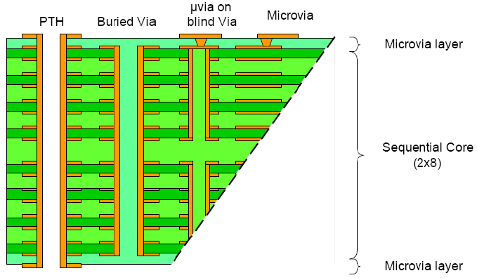 Figure 31: Simplified build-up of HDI PCB
high speed signal
electronic functionality that requires specific design precautions to maintain time dependant signal integrity
This is further specified in IPC-2251 and IPC-2141A.
hole wall pull away
adhesion defect between copper of the hole wall and resin
HTE
grade of copper foil with the grade designation “high temperature elongation electrodeposited”
This is specified in IPC-4562A.
intralayer
within the same layer in X,Y direction
interlayer
in between two superpositioned layers in Z direction
JTC
grade of copper foil
This grade of copper foil is produced by GOULD Electronics GmbH.
laminate
sheets of fully cured, C-stage, resin with copper cladding
Rigid laminate includes reinforcement, for example by woven glass fibres or non-woven aramid fibres.
microvia
blind via manufactured by laser ablation with a diameter smaller than conventional vias.
- 1 Microvias are required for routing internal signals in HDI PCBs.
- 2 Example of microvia configuration is shown in Figure 31.
microvia layers
layers of conductive pattern that contain microvias
microvia layers are layers 1 and 2 and opposite layers
mil
unit of length equal to 25,4 µm
The unit mil is in some cases customary in PCB design and therefore preferred above the SI unit.
no-flow prepreg
type of prepreg that has a reduced flow of resin during press cycle
The term “low-flow prepreg” is synonymous with the word “no-flow prepreg”. The terms do not specify the exact amount of flow.
non-functional pad
pad on internal copper layer without electrical connection
non-plated hole
hole in a PCB that does not contain plating or other type of conductive reinforcement
normal pitch
standard spacing of tracks and pads
See “fine pitch” for another category of pitch.
number of layers
number of layers in a PCB containing conductive elements
* For example, the numbering convention is from top to bottom layer: L1, L2, …,Ln-1, Ln.
panel
area of laminated layers that contains PCBs and coupons processed as a single unit
PCB manufacturer
entity that manufactures the PCB
peelable
areas of photo resist or copper that have poor adhesion to underlying substrate because of a tapered shape with a narrow dimension on one end
plated through-holes (PTH )
metal-plated holes drilled through all the layers used for assembly of components
printed circuit board (PCB)
product resulting from the process of selectively etching unwanted copper from surfaces of copper clad insulating substrates to form a desired circuitry pattern which is metal-plated and laminated
Examples of specific PCB technologies are rigid, flexible, rigid-flex, double sided, multilayer, sequential, RF and HDI PCBs
prepreg
sheets of partly cured, B-stage, resin with reinforcement
Examples of reinforcement are woven glass fibres and non-woven aramid fibres.
RF elements
conductive pattern on PCB with specific RF functionality
For example filters, combiners, splitters, couplers. RF elements do not have voltage ratings or solder connections.
resin starvation
region in a PCB that has an insufficient amount of resin to wet out completely the reinforcement
This is shown by low gloss, dry spots or exposed fibres.
review item
design feature to be included into the PCB definition dossier and reviewed during the PCB design review
projected peak-to-peak insulation distance
worst-case minimum thickness of dielectric material that includes thickness tolerance of the laminate core and the maximum roughness of copper surface treatment
Figure 32 specifies how this is measured.
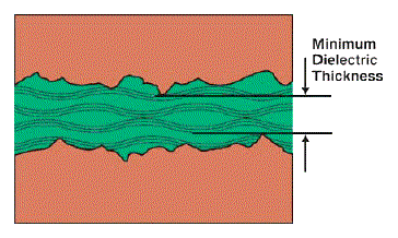 Figure 32: Projected peak-to-peak insulation distance
serialization
process of numbering of each unique PCB by the PCB manufacturer for traceability
sliver
pieces of photo resist or copper that have poor adhesion to underlying substrate because of the small surface area.
For example, a surface area below 0,01 mm2
soldering pad
conductive part intended for soldering components on the PCB
spacing
insulation distance
The term “gap” is synonymous with the word “spacing”, but this term is not used in the present standard.
stack
assembly comprising of one sequence of laminated layers
Half-stack identifies the sub-assembly.
test pad
pad that is dedicated for electrical testing on the PCB
track
conductive part routing the electrical connection between the pads
The term “line” and the term “conductive track” are synonyms with the word “track”
via
metal-plated hole drilled through all layers, only used for interconnection between layers
A via is not used for assembly
X,Y direction
orientation in the plane of the PCB, along length and width of the PCB
Z direction
orientation perpendicular to the plane of the PCB, along height of the PCB
Abbreviated terms
For the purpose of this Standard, the abbreviated terms from ECSS-S-ST-00-01 and the following apply:
|
Abbreviation
|
Meaning
|
|
AAD
|
area array device
|
|
AC
|
alternating current
|
|
AOI
|
automated optical inspection
|
|
BGA
|
ball grid array
|
|
CAD
|
computer aided design
|
|
CAE
|
computer aided engineering
|
|
CGA
|
column grid array
|
|
CIC
|
Copper – Invar - Copper
|
|
CoC
|
certificate of conformance
|
|
CRC
|
cyclic redundancy check
|
|
CTE
|
coefficient of thermal expansion
|
|
Cu
|
copper (element)
|
|
DC
|
direct current
|
|
DRD
|
document requirements definition
|
|
DWV
|
dielectric withstanding voltage
|
|
GND
|
electrical signal to ground
|
|
EMC
|
electromagnetic compatibility
|
|
FAI
|
first article inspection
|
|
FP
|
flat pack
|
|
FR4
|
type of epoxy resin for PCBs
|
|
HDI
|
high density interconnect
|
|
i.a.w.
|
in accordance with
|
|
I/O
|
input/output
|
|
LCC
|
leadless chip carrier
|
|
LF
|
low frequency
|
|
MRR
|
manufacturing readiness review
|
|
PCB
|
printed circuit board
|
|
PID
|
process identification document
|
|
ppm
|
parts per million (10-6)
|
|
PTH
|
plated through hole
|
|
PTFE
|
polytetrafluoroethylene
|
|
QFP
|
quad flat pack
|
|
RF
|
radio frequency (high frequency)
|
|
SOIC
|
small outline integrated circuits
|
|
SPF
|
single point failure
|
|
sq
|
square (in unit Ω/sq)
|
|
TDR
|
time domain reflectometry
|
|
Tg
|
temperature of glass transition
|
|
Th
|
thickness
|
|
Vcc
|
power supply voltage
|
|
Vrms
|
voltage root mean square
|
Principles
Qualified PCBs
Qualified PCBs for space application meet the following conditions:
PCB is procured in conformance with requirements of ECSS-Q-ST-70-11,
PCB is procured from a PCB manufacturer that is qualified in conformance with requirements of ECSS-Q-ST-70-10,
the PCB technology is qualified in conformance with requirements of ECSS-Q-ST-70-10 for that PCB manufacturer,
the PCB design is in conformance with the requirements of ECSS-Q-ST-70-12, and
the PCB design, the manufacturing process and materials are in conformance with the PID of the PCB manufacturer.
PA requirements of space projects use this standard as applicable document. Based on their heritage, suppliers can propose the re-use of existing PCB designs that are “recurrent” and that are not in compliance with all design requirements of this standard. The possible acceptability of those cases is reviewed by the project on case by case basis. The PCB design is “recurrent” only when no changes are made in the artwork, routing, lay-out, build-up, material selection.
Manufacturing tolerances
Dimensional measurements of PCBs are “as-designed” except when explicitly mentioned “as-manufactured”.
Design values are affected by the manufacturing tolerances. The minimum value on the PCB as-manufactured equals the design value subtracted with the manufacturing tolerance. See definition of terms in clause 3.2.
Reliability of design
Specific design features of PCBs are recorded as Review Items in the PCB definition dossier. This is done when the design features include a higher technological complexity that can affect manufacturability or (thermal) reliability. These design features are specifically evaluated by qualification prior to inclusion in the PID.
Requirements in this standard generally state minimum dimensions permitted. It is good practice to use minimum dimensions only when necessary to achieve the desired functionality and to design with margin when possible. For instance, it is recommended to implement minimum insulation distance between tracks only when space limitations prevent larger insulation distance. It is recommended to implement fan out of tracks which allows for larger insulation distances where more space is available.
The robustness of the PCB can be affected when combining multiple design features at the limit of the requirement or recorded as Review Item. The PCB manufacturer and the supplier evaluate this risk during the design review and provide formal approval during the MRR. The reliability of the manufactured PCB is evaluated by inspection on representative coupons.
Design review and MRR
Overview
This clause specifies the iterative process of designing a PCB in collaboration with the PCB manufacturer and specifies associated documentation for the formal authorization for manufacture.
Documentation
The supplier shall issue the PCB definition dossier in conformance with the DRD in Annex A.
The supplier shall list design features as Review Items in conformance with clause A.2.1<7> from the DRD of the Annex A.
The supplier may list other design features as Review Items .
The supplier shall submit the PCB definition dossier to the PCB manufacturer for the design review.
The supplier should submit to the PCB manufacturer the draft PCB definition dossier or a list of specific Review Items specified in the requirement 5.2b in the design phase, when those Review Items are at the limit of the PID capability.
Examples of Review Items that can be on the limit of PID capability are: dimensions, number of layers, maximum aspect ratio, number of sequences, material selection or a combination of these. Consultation with PCB manufacturer at this early design stage is recommended to avoid unnecessary risks. Multiple iterations can be performed to achieve an agreed PCB definition dossier.
The PCB manufacturer shall review the PCB definition dossier including Review Items for compliance with the PID.
As a result of the design review, the PCB manufacturer may identify to the supplier additional Review Items in the PCB definition dossier.
Review Items can exist for PCB designs even within the capability of the PID. These Review Items and methods to mitigate them are specified in this standard as best practices and recommendations.
The PCB manufacturer shall provide the PCB manufacturing dossier in conformance with DRD in the Annex B.
The PCB manufacturer shall issue to the supplier a MRR checklist, which is part of the PCB manufacturing dossier, in conformance with the DRD in the Annex B.
An example of a MRR checklist is given in Annex G.
During the MRR, supplier and PCB manufacturer shall approve the PCB manufacturing dossier, the PCB definition dossier and all Review Items.
The approvals are recorded in the MRR checklist.
The MRR shall provide authorisation for manufacture to the PCB manufacturer.
General design and production requirements
Reliability of design
The supplier shall design the PCB with margin.
This is also described in clause 4.3.
Choice of materials and build-up
Overview
For the selection of materials for PCB a number of physical properties are important, such as Tg, Young’s modulus, dielectric constant, CTE, hygroscopy. Table 61 provides an overview of some commonly used materials and their physical properties. The CTE of the as-manufactured PCB depends on the total copper thickness, which has a CTE of about 16 ppm/K.
It is important that for the selection of the technology for the PCB design the following is taken into account:
CTE mismatch between devices and PCB,
moisture sensitivity of PCB function,
interconnection constraints,
lay-out constraints.
Rigid-flex boards can be preferred to reduce the interconnection constraints.
Polyimide and epoxy are the most commonly used materials. Polyimide has an advantage over epoxy because it is more thermally stable and outperforms epoxy in thermal cycling and assembly. At the same time, polyimide is more hygroscopic than epoxy, which affects PCB ground use and assembly. Epoxy is available with different glass transition temperatures (Tg). Higher glass transition temperature is recommended for epoxy because it provides better thermal stability. Thermal expansion of resin in Z direction below and above Tg is typically higher than expansion of copper. Therefore it is beneficial for thermal endurance to use materials with low CTE in Z direction. Flame retardants in base materials are commonly required for ground based applications but are not necessary for space based PCBs.
For high frequency performance typically PTFE based materials are used. These materials require special lamination cycles as adhesion is generally poorer compared to polyimide and epoxy.
IPC-4121 provides a comparison of various properties for core constructions as function of resin and glass type.
Table 61: Characteristics of some example dielectric materials for laminates
|
Type of material
|
Dielectric constant
|
Dissipation Factor
|
Tg (°C)
|
water absorption (%)
|
Volume density (g/cm3)
|
CTE (ppm/K)
|
CTE (ppm/K)
|
Thermal conductivity (W/m.K)
|
Example
| ||||||
|
at 1 MHz
|
at 10 GHz
|
at 1 MHz
|
at 10 GHz
|
|
|
|
X
|
Y
|
Z
|
X
|
Y
|
Z
|
|
|
|
|
Epoxy HTg
|
4,24
|
3,92
|
0,015
|
-
|
180
|
0,15
|
-
|
13 - 14
|
13 - 14
|
45
|
14 - 17
|
14 - 17
|
230
|
0,4
|
370 HR
|
|
4,24
|
3,92
|
0,015
|
-
|
170
|
0,15
|
-
|
13 - 14
|
13 - 14
|
45
|
14 - 17
|
14 - 17
|
230
|
0,4
|
IS420 (Isola)
| |
|
Polyimide / Glass
|
4,2
|
-
|
0,01
|
-
|
> 250
|
0,26
|
1,6
|
16
|
16
|
51
|
-
|
-
|
158
|
0,2
|
35N (Arlon)
|
|
4,2
|
-
|
0,01
|
-
|
250
|
0,27
|
1,6
|
16
|
16
|
55
|
-
|
-
|
149
|
0,2
|
85N (Arlon)
| |
|
Polyimide / Aramid
|
3,6
|
-
|
0,014
|
-
|
250
|
0,6
|
1,37
|
6 - 9
|
6 - 9
|
93
|
-
|
-
|
279
|
0,2
|
85NT (Arlon)
|
|
Polyimide flex laminate
|
3,4
|
3,3
|
0,003
|
-
|
220
|
0,8
|
-
|
25
|
25
|
-
|
-
|
-
|
-
|
-
|
AP (DuPont)
|
|
Ceramic reinforced PTFE
|
-
|
2,94
|
-
|
0,0012
|
-
|
0,02
|
2,1
|
16
|
16
|
24
|
-
|
-
|
-
|
0,6
|
RT/Duroid 6002 (Rogers)
|
|
Hydrocarbon and ceramic reinforced glass
|
-
|
3,38
|
-
|
0,0027
|
> 280
|
0,06
|
1,79
|
11
|
14
|
46
|
-
|
-
|
-
|
0,71
|
RO 4003 (Rogers)
|
|
Glass reinforced PTFE
|
2,20
|
2,20
|
0,0004
|
0,0009
|
-
|
0,02
|
2,2
|
31
|
48
|
237
|
-
|
-
|
-
|
0,2
|
RT/Duroid 5880 (Rogers)
|
|
Ceramic thermoset
|
-
|
9,8
|
-
|
0,002
|
-
|
0,16
|
2,77
|
19
|
19
|
20
|
-
|
-
|
-
|
0,76
|
TMM10i (Rogers)
|
Material selection
Selection of the base laminate materials shall be performed in compliance with the requirements from the clause 5.2.1 of the ECSS-Q-ST-70-11.
The material selection for all types of PCBs shall be in compliance with the requirements from the clauses 7.1 to 7.6 of the ECSS-Q-ST-70-11.
Examples of types of PCBs are: single sided, double sided, multilayer, sequential, rigid, rigid-flex, flexible, sculptured flex, HDI, RF.
The as-manufactured PCB shall be in conformance with the outgassing requirements of the clause 5.5.3 from the ECSS-Q-ST-70-02 or project specific requirements on cleanliness.
The outgassing requirements are CVCM<0,1% and RML<1,0%.
Selection of the PCB manufacturer
The supplier shall procure PCBs from a PCB manufacturer with a qualification approval for an identified technology in conformance with the requirements from the clause 5 to clause 9 of the ECSS-Q-ST-70-10.
The supplier shall procure the PCBs in conformance with the requirements from the clause 5 to clause 7 of the ECSS-Q-ST-70-11.
Traceability and marking
The PCB shall be marked with part number and revision number from the PCB definition dossier as given by the supplier.
All individual PCBs within the panel shall be identified by a serial number.
The serialization of the PCB shall be established before the start of the fabrication.
The serial number shall identify the position of the PCB on the panel.
The serial number methodology shall be identified in the PID of the PCB manufacturer.
Rigid PCBs
PCB build-up
General
The build-up of the PCB and each sub-assembly should be symmetric.
This is done to avoid warp and twist.
The supplier shall record asymmetric build-up as a Review Item in the PCB definition dossier.
The build-up includes the copper thickness and its distribution.
In case Molybdenum or CIC layers are used, they shall be included in the build-up and recorded as a Review Item in the PCB definition dossier.
- 1 Specific requirements for the build-up are listed in the PCB definition dossier in A.2.1<5>a.3(h).
- 2 On external layers, copper clad laminate typically achieves better peel strength whereas copper foil achieves better registration.
Copper styles
The thickness of the copper cladding on both sides of the laminate should be equal except on outer layers of the PCB or half-stack.
Equal copper thickness is needed when laminate is etched in same process steps, as is the case for internal layers. The exception on outer layers is made because each side is etched in different process steps and because thin copper on external layers decreases the total thickness after plating.
In case the thickness of the copper cladding on the laminate is asymmetric, this asymmetric build-up of the PCB shall be recorded as a Review Item in the PCB definition dossier.
17/70 copper thickness is more risky than 17/35 or 35/70 copper thickness. The presence of fine pitch tracks in combination with asymmetric copper further increases the difficulty to process.
Except the case specified in the requirement 11.4.1e, the external and internal layers shall use basic copper thickness 70 µm, 35 µm or 17 µm.
- 1 Copper layers can be implemented as copper clad laminate or as separate copper foils.
- 2 Requirement 11.4.1e specifies microvia layers on HDI PCBS.
Copper distribution within a layer should be homogeneous.
This is done to ensure even pressure distribution during lamination, which can cause filling voids, cracks or glass compression.
Balancing of copper should be performed by including dummy non-functional copper.
This is more important for partial planes on thick copper layers such as 70 µm.
Signal tracks should not be routed on copper plane layers.
In case the total as-designed thickness of copper is above 700 µm, this shall be recorded as a Review Item in the PCB definition dossier.
High layer count in combination with thick copper layers can have significant impact on manufacturability and long-term reliability.
Copper quality “HTE” shall be used for copper clad laminate.
Type HTE can be procured in conformance with IPC-4562 Type E, grade 3.
Copper quality “JTC” or “HTE" shall be used for copper foils.
The values from the Table 71 should be used in the design calculations for copper foil thickness.
The values indicated in Table 71 are minimum as-manufactured thickness for the specified as-designed foil thickness.
Table 71: As-designed versus as-manufactured copper foil thickness
|
As-designed foil thickness
|
Minimum as-manufactured thickness for non-plated inner layers
|
Minimum as-manufactured thickness for plated layers with ≥25 µm plating
|
|
9
|
6
|
31
|
|
12
|
9
|
34
|
|
17
|
11
|
38
|
|
35
|
25
|
53
|
|
70
|
56
|
84
|
Dielectric thickness
A minimum of two sheets of prepreg shall be used for insulation between two layers.
A minimum of two sheets of glass should be used in glass-reinforced laminates.
In case a single sheet of glass is used in a glass-reinforced laminate it shall be recorded as Review Item in the PCB definition dossier.
Two sheets of glass reinforcement are specified to mitigate the risk of reduced insulation caused by contamination. This is also specified for laminates for class 3/A in accordance with IPC-6012 Appendix A. In case a single reinforcement in laminate is used, it is recommended to implement other means to mitigate the risk of contamination in laminate. IPC-4121 provides various properties, such as resin-to-glass ratio, for core laminate constructions.
The insulation distance as-designed between two layers in rigid laminate or prepreg in Z direction should be in conformance with the values from Table 137.
This table specifies a minimum distance of 100 µm.
Except the case specified in the 11.4.1h, the insulation distance as-manufactured between two layers in rigid laminate or prepreg in Z direction shall be in conformance with the values from Table 137.
- 1 This table specifies a minimum projected peak-to-peak distance of 70 µm.
- 2 Requirement 11.4.1h specifies microvia layers on HDI PCBs..
Double-sided copper clad laminate with a thickness as-designed of 4 mil (100 µm) shall not be used unless: - the voltage is less than 30V,
- the copper foil thickness on both sides of the laminate is 17 µm or 35 µm,
- the laminate batch is screened by the PCB manufacturer to have a nominal thickness of the etched laminate of ≥ 3,8 mil,
- the insulation distance as-manufactured is verified by the PCB manufacturer to be in compliance with requirement 7.1.3e, and
- it is recorded as a Review Item in the PCB definition dossier.
- 1 Requirement 7.1.3f.1 is in compliance with the values from Table 133.
- 2 The nominal thickness of etched laminate from the requirement 7.1.3f.3 can be read from the CoC. However, this does not indicate worst-case thickness as mentioned in the requirement 7.1.3e. Therefore the use of 4 mil laminate on the lower end of the tolerance between 3,5 mil and 3,8 mil is prohibited by this requirement.
- 3 The precautions specified in this requirement are defined to prevent a worst-case insulation value of less than 70 µm due to high tolerances with rough copper surface treatment as indicated in Table 72.
Double-sided copper clad laminate with a thickness as-designed of 5 mil (125 µm) shall not be used above 30 V unless: - the thickness of laminate as-manufactured is in conformance with the Table 133,
- the laminate batch is screened by the PCB manufacturer to have a nominal thickness of the etched laminate of ≥ 4,8 mil,
- the as-manufactured insulation distance is verified by the PCB manufacturer to be in compliance with requirement 7.1.3g.1,
- it is recorded as a Review Item in the PCB definition dossier.
- 1 The thickness value of the requirement 7.1.3g.1 is ≥100 µm.
- 2 This value specified in the requirement 7.1.3g.2 can be read from the CoC. It does not indicate worst-case thickness as mentioned in the requirement 7.1.3g.1. This prohibits the use of 5 mil laminate on the lower end of the tolerance between 4,5 mil and 4,8 mil.
- 3 Precautions specified in this requirement are defined to prevent a worst-case insulation value of less than 100 µm due to high tolerances with rough copper surface treatment as indicted in Table 72.
For insulation distance in Z direction of a laminate, the minimum projected peak-to-peak insulation distance specified in the requirement 7.1.3i shall be used.
The minimum projected peak-to-peak insulation distance shall include the thickness tolerance of the laminate core and the maximum roughness of copper surface treatment.
Projected peak-to-peak insulation distance is specified in Figure 3-1 of IPC-4101.
If available, laminates should be class D in conformance with requirements from the IPC-4101 except the cases specified in the requirement 7.1.3k.
- 1 Class D guarantees a minimum projected peak-to-peak insulation distance.
- 2 Typically used materials can be unavailable in class D even though this specification exists.
In case other laminate classes are used, the PCB manufacturer shall calculate minimum projected peak-to-peak insulation distance in conformance with requirement 7.1.3i.
An example of this is shown in Table 72 for class C laminate and commonly used copper profiles.
The PCB manufacturer shall define laminate and prepreg styles and amount to achieve the insulation distances as designed by the supplier in conformance with requirements of the clause 13.8.
The supplier is responsible to design insulation distances required to meet design voltages in conformance with the requirement 13.8.2c.
Table 72: Example of worst case as-manufactured insulation distance for laminate with double-sided copper cladding
|
As-designed laminate thickness
|
Laminate thickness tolerance i.a.w. IPC4101 Table3.7 class C.
|
Copper foil 18 or 35 µm
|
Copper foil 70 µm
| ||
|
“Very low profile” i.a.w. IPC4562 Table3.1
|
Worst-case as-manufactured projected peak-to-peak insulation distance
|
“Low profile” i.a.w. IPC4562 Table3.1
|
Worst-case as-manufactured projected peak-to-peak insulation distance
| ||
|
101,6 µm
|
±13 µm
|
5,1 µm
|
78,4 µm
|
10,2 µm
|
68,2 µm
|
|
127 µm
|
±18 µm
|
5,1 µm
|
98,8 µm
|
10,2 µm
|
88,6 µm
|
|
152 µm
|
±18 µm
|
5,1 µm
|
123,8 µm
|
10,2 µm
|
113,6 µm
|
|
203 µm
|
±25 µm
|
5,1 µm
|
167,8 µm
|
10,2 µm
|
157,6 µm
|
|
254 µm
|
±25 µm
|
5,1 µm
|
218,8 µm
|
10,2 µm
|
208,6 µm
|
PCB dimension
The maximum dimensions of the PCB depend on the panel dimensions used and qualified by the PCB manufacturer. A typical large panel size is 45x60 cm (18x24 inch). Not all surface area of the panel is available for the PCB design as mandatory coupons are included in the panel.
Thickness of PCB
General
PCB thickness shall be measured from bottom insulation to top insulation.
- 1 The manufacturing tolerance is provided by the PCB manufacturer.
- 2 It is important to include the manufacturing tolerance of 10% in conformance with the requirement 7.6.b.2 from the ECSS-Q-ST-70-11.
- 3 Tolerances on individual copper clad laminate of 100 µm is about ± 18%. Tolerance on the total PCB stack is typically lower.
- 4 Specific requirements for maximum thickness over metal surface finish are specified in the PCB definition dossier.
Polyimide PCB
The thickness as-manufactured of a rigid and rigid-flex polyimide PCB shall be ≤ 4,0 mm.
The as-designed thickness of a rigid and rigid-flex polyimide PCB should be ≤ 3,6 mm, except the case specified in the requirement 7.3.2c.
The as-designed thickness of a rigid and rigid-flex polyimide PCB may be > 3,6 mm in case:
- the thickness as-manufactured is in conformance with requirement 7.3.2a,
- the manufacturing tolerance is < 10%, and
- it is recorded as a Review Item in the PCB definition dossier.
Epoxy PCB
The thickness as-manufactured of a rigid and rigid-flex epoxy PCB shall be ≤ 2,4 mm.
The as-designed thickness of a rigid and rigid-flex epoxy PCB should be ≤ 2,2 mm, except the case specified in the requirement 7.3.3c.
The as-designed thickness of a rigid and rigid-flex epoxy PCB may be >2,2 mm in case:
- the thickness as-manufactured is in conformance with requirement 7.3.3a,
- the manufacturing tolerance is < 10%, and
- it is recorded as a Review Item in the PCB definition dossier.
Number of copper layers in PCB
Number of copper layers for polyimide PCB shall be ≤ 26.
Number of copper layers for epoxy PCB shall be ≤ 20.
Aspect ratio of vias
Except the case specified in the requirement 11.5.6a, the aspect ratio of vias on a rigid and rigid-flex PCB shall be ≤ 7.
- 1 There is no additional requirement for the minimum diameter of plated via in case the diameter conforms to the aspect ratio of ≤ 7.
- 2 Requirement 11.5.6a specifies aspect ratio for AAD with 1 mm pitch on HDI PCBs.
Track width and spacing
General
A verification should be performed to prevent non-functional changes of direction of tracks.
Some automated routing software can cause unnecessary changes of direction that have no function.
Manufacturing tolerances for width and spacing
The relative manufacturing tolerances on the track width and spacing of internal and external layers shall be as specified in Table 73.
The maximum absolute manufacturing tolerances on the track width and spacing of internal and external layers shall be as specified in Table 73.
- 1 For example, an internal track width of 400 µm on 35 µm copper thickness has a relative tolerance of ± 20 %, i.e. 80 µm, which is limited by the maximum absolute tolerance of 50 µm.
- 2 The tolerance applies to as-designed dimensions. For example, a spacing as-designed of 200 µm with a tolerance of ± 20 % results in a spacing as-manufactured of 160 µm - 240 µm. Typically, the minimum spacing of 160 µm is important for PCB design.
The use of planarization, copper reduction or surface preparation processes shall be excluded in the definition of the total copper thickness. - 1 Plating of sequential half stacks can be done with different plating methods, like panel plating, selective pattern plating or a combination and can include copper surface reduction processes to reduce copper surface thickness and give best options for fine pitch etching.
- 2 The plated copper thickness as-designed is 25 µm. This can be a thicker layer as-manufactured.
Table 73: Tolerance on track width and spacing of internal and external layers
|
Thickness category [µm]
|
Basic Cu
|
Plated Cu
|
Total Cu thickness
|
Relative tolerance on track width and spacing
|
Maximum absolute tolerance on track width and spacing
|
|
Th17
|
≤ 17
|
0
|
≤ 17
|
± 20 %
|
± 30 µm
|
|
17<Th60
|
≤ 17
|
1x25
|
≤ 42
|
± 20 %
|
± 50 µm
|
|
35
|
0
|
35
| |||
|
35
|
1x25
|
60
| |||
|
60<Th70
|
≤ 17
|
2x25
|
≤ 67
|
± 50 µm
| |
|
70
|
0
|
70
| |||
|
70<Th95
|
35
|
2x25
|
85
|
± 70 µm
| |
|
70
|
1x25
|
95
| |||
|
Note: Explanation of "FOR" is given in Table 131.
| |||||
External layers
The as-manufactured track width and spacing as a function of copper thickness for external layers of rigid PCB shall be in conformance with the values specified in the Table 74.
The as-designed track width and spacing for external layers of rigid PCB should be in conformance with the values specified in the Table 137 except the case specified in the requirement 7.4.3c.
In case the as-designed track width and spacing for external layers of rigid PCB is less than the values specified in the requirement 7.4.3b, the following conditions shall be met:
- the manufacturing tolerances as specified in the PID are smaller than as specified in Table 73,
- the as-manufactured dimensions specified in Table 74 and Table 137 are met, and
- it is recorded as a Review Item in the PCB definition dossier.
Tracks should not be routed on external layers.
In case tracks are routed on external layers they should not be routed under components.
The basic copper foil thickness of fine pitch shall be 17 µm.
Fine pitch track width and spacing may be used in case: - fine pitch tracks are used to route to the footprint of a fine pitch component,
- the length of fine pitch tracks is ≤ 20 mm from the solder pad,
- conformal coating is applied on fine pitch tracks or pads in conformance with the requirement 13.8.4b,
- the voltage is ≤ 30V, and
- it is recorded as a Review Item in the PCB definition dossier.
A long fine pitch track can cause solder pearls.
Spacing and width of pads shall be in conformance with the requirements for tracks specified in 7.4.3a, 7.4.3b, 7.4.3c, 7.4.3f and 7.4.3g.
Table 74: Minimum as-manufactured track width and spacing for external layers as a function of copper thickness
|
Basic Cu
|
Plated Cu
|
Thickness category [µm]
|
Pitch
|
As-manufactured
| |
|
width [µm]
|
spacing [µm]
| ||||
|
17
|
1x 25
|
17<Th60
|
fine/normal
|
120/160
|
120/160
|
|
17
|
2x 25
|
60<Th70
|
fine/normal
|
120/160
|
120/160
|
|
35
|
1x25
|
17<Th60
|
normal
|
160
|
160
|
|
35
|
2x25
|
70<Th95
|
normal
|
240
|
240
|
|
70
|
1x25
|
70<Th95
|
normal
|
240
|
240
|
Normal pitch tracks on internal layers
The as-manufactured track width and spacing as a function of copper thickness for internal layers of rigid PCB shall be in conformance with the values specified in the Table 75.
The as-designed track width and spacing for internal layers of rigid PCB should be in conformance with the values specified in the Table 137 except the case specified in the requirement 7.4.4c.
In case the as-designed track width and spacing for internal layers of rigid PCB is less than the values specified in the requirement 7.4.4b, the following conditions shall be met:
- the manufacturing tolerances as specified in the PID are smaller than as specified in Table 73,
- the as-manufactured dimensions specified in Table 75 and Table 137 are met, and
- it is recorded as a Review Item in the PCB definition dossier.
The thickness category of copper on internal layers shall be as specified in Table 73.
Table 75: Minimum as-manufactured track width and spacing for internal layers as a function of copper thickness
|
Thickness category[µm]
|
Pitch
|
As-manufactured
| |
|
width [µm]
|
spacing [µm]
| ||
|
Th17
|
fine/normal
|
80/104
|
96/104
|
|
17<Th60
|
normal
|
120
|
120
|
|
60<Th70
|
normal
|
160
|
160
|
|
70<Th95
|
normal
|
240
|
240
|
Fine pitch tracks on internal layers
Except the case specified in the requirement 11.5.5a, the track width and spacing for fine pitch on internal layers shall be in conformance with the as-manufactured dimensions specified in Table 75.
Requirement 11.5.5a specifies track width and spacing for impedance controlled routing to AAD with 1 mm pitch on HDI PCBs .
In case fine pitch tracks are used, this shall be recorded as a Review Item in the PCB definition dossier.
Fine pitch shall be limited to the functionality of impedance control or signal routing to AAD.
Fine pitch tracks shall be limited to ≤ 30 V.
For routing to AAD, fine pitch tracks shall fan out to normal pitch as soon as they are outside the AAD footprint.
In case no other circuitry is adjacent that requires the use of fine pitch, the routing of fine pitch tracks shall increase the insulation distance and track width as specified for normal pitch in the Table 75.
- 1 CAD software can implement different minimum insulation distances and track widths in areas with different space available.
- 2 The Figure 71 shows examples of possible improvements in routing.
Fine pitch shall be manufactured by using 17 µm basic copper thickness without plating steps.
Routing to AAD footprint on internal layers
Tracks in AAD footprint shall be placed equidistant between pads to increase insulation distance to both pads.
See example of nonconformance indicated by blue arrow in Figure 71.
Tracks shall exit from AAD footprint before changing direction to keep the insulation distance to the pad in compliance with normal pitch as specified in Table 75.
See example of nonconformance indicated by green arrow in Figure 71.
Widening of tracks shall occur close to AAD footprint to provide a wider track where no other circuitry is adjacent that requires the use of fine pitch.
See example of nonconformance indicated by yellow arrow in Figure 71.
Changing of direction of track should be in compliance with the requirement 7.4.1a.
See example of nonconformance indicated by white arrow in Figure 71
Pads of AAD footprint may be designed with teardrop reinforcement
Pads in Figure 71 are not designed with teardrop reinforcement.
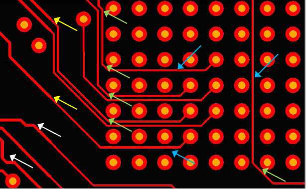 Figure 71: Example of automated fine pitch routing and possible improvements
Pad design
Non-functional pad removal
Non-functional pads shall be present on all layers, except two cases specified in the requirement 7.5.1b.
The presence of non-functional pads reduce the risk of hole wall pull-away and reduce the risk of cracks in resin-rich areas.
Non-functional pads may be removed:
- when the presence of the pads degrade the electrical performance, they can be removed by the supplier, or
- to prevent high pressure area during lamination that cause resin starvation in the prepreg, the pads can be removed by the PCB manufacturer.
Removal of non-functional pads is approved by supplier and PCB manufacturer during MRR in conformance with the requirement 7.5.1c.6
When non-functional pads are removed as specified in the requirement 7.5.1b, the following conditions shall be met:
- non-functional pads are present on all copper plane layers,
- non-functional pads are present on flex laminate,
- maximum half of the non-functional pads in the pad stack are removed,
- non-functional pads are removed on maximum two consecutive layers,
- non-functional pads are removed on maximum one side of a laminate, and
- it is recorded as a Review Item in the PCB definition dossier. Non-functional pads should not be removed on layer 2 and n-1.
Pad dimensions
Except the case specified in the requirement 11.5.2a, the annular ring as-manufactured on internal layers shall be in conformance with the requirement 9.5.b.15(d) of ECSS-Q-ST-70-10.
- 1 This requirement specifies 50 µm.
- 2 Requirement 11.5.2a specifies annular ring of internal pads for fine pitch footprint on HDI PCBs.
The annular ring as-manufactured on component side of external layers shall be in conformance with the requirement 9.5.b.15(b) of ECSS-Q-ST-70-10.
This requirement specifies 100 µm.
Except the case specified in the requirement 7.5.3b.2, the annular ring as-manufactured on solder side of external layers shall be in conformance with the requirement 9.5.b.15(a) of ECSS-Q-ST-70-10.
This requirement specifies 200 µm
For component holes on solder side the minimum diameter of external pads should be the diameter of as-manufactured hole plus ≥ 0,8 mm.
For component holes on solder side the minimum diameter of external pads may be the diameter of as-manufactured hole plus ≥ 0,6 mm in case:
- the as-manufactured annular ring as specified in the requirement 7.5.2c,
- the component holes are a footprint for a nano D connector,
- it is recorded as Review Item in the PCB definition dossier.
For via holes and component holes on component side the diameter of external pads should be the diameter of as-manufactured hole plus ≥ 0,6 mm.
For via holes and component holes on component side the diameter of external pads may be the diameter of as-manufactured hole plus ≥ 0,5 mm in case: - the as-manufactured annular ring as specified in the requirement 7.5.2b, and.
- it is recorded as a Review Item in the PCB definition dossier. The diameter of internal pads should be the diameter of drilled hole plus ≥ 0,3 mm.
- 1 The drilled diameter is typically 0,2 mm larger than the as-manufactured minimum hole diameter.
- 2 It is important to consider the number of drilling and lamination sequences and the PCB manufacturing tolerances for the design of the diameter of the pads.
The diameter of pads may be the diameter of the drilled hole plus < 0,3 mm in case this is recorded as a Review Item in the PCB definition dossier.
Tear drop reinforcement of pads to tracks can be used for a more robust design and to mitigate the risk of a smaller designed diameter.
Non-circular external pads
Pads for component holes on external layers shall be circular, except cases specified in the requirement 7.5.3b.
Non-circular pads may be used for component holes, in case the following conditions are met:
- the surface area of the oblong pad is not smaller than the surface area of the circular pad as specified in the requirements from the clause 7.5.2,
- the oblong pad meets the requirement for annular ring of 100 µm as-manufactured, and
- it is recorded as a Review Item in the PCB definition dossier.
- 1 For the requirement 7.5.3b.1 A(oblong) in Figure 72 is the surface area of the oblong pad and A(circular) in Figure 72 is the surface area of a circular pad
- 2 For the requirement 7.5.3b.2 see Annular ring(oblong) in Figure 72
- 3 The design in the requirement 7.5.3b.2 is a deviation of the requirement 7.5.2c (and ECSS-Q-ST-70-10 requirement 9.5b.15.a) of 200 µm annular ring for pads on solder side (see Annular ring(circular) in Figure 72) in one direction, compensated by a larger annular ring in the other direction.
- 4 Other non-circular pad designs are possible and typically used on external layers for AAD and SMT components. Dog-bone shapes or key hole shapes can be used for the verification of solder joint quality or to prevent thermal stress on (blind or micro) vias.
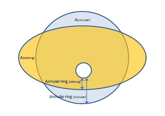 Figure 72: Comparison between circular and oblong pads showing annular ring and the centre of the hole misregistered with the centre of the pad
Copper planes in rigid PCB
Copper planes should have additional openings in a grid format.
- 1 For example, planes larger than 10 cm2 can be designed using a grid.
- 2 An example of a grid plane is shown in Figure 73.
The grid should be offset between layers.
These additional openings act as venting holes for desorption of humidity out of the PCB. For example, a grid can be 0,4 mm lines at a pitch of 0,6 mm and at 45° angle. The thermal and electrical resistance across such hatch plane is a factor of 2,5 larger than across a solid plane, assuming pattern as specified above. This can affect both power distribution and signal integrity, in particular for RF or digital PCB.
For partial copper planes, balancing of copper should be performed in conformance with requirements 7.1.2d and 7.1.2e.
Copper layers should be placed symmetrically within the build-up.
This is done to limit warp and twist.
In case copper layers are placed asymmetrically within the build-up, this shall be recorded as a Review Item in the PCB definition dossier.
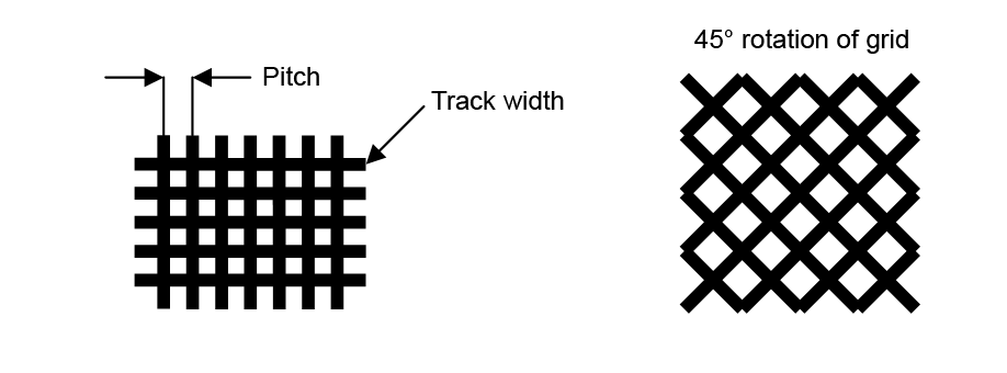 Figure 73: Grid copper plane with openings
Design considerations for the prevention of sliver and peelable
All areas of the conductive patterns as well as areas of insulating dielectric shall have a dimension of ≥ 0,1 mm in X and Y direction after etch compensation.
This is done to prevent sliver or peelable see Figure 74.
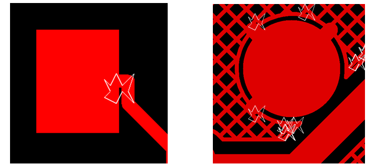 Figure 74: Example of peelable (left) and sliver (right)
PCB surface finish
Metallization
Plating of metallic layers and finishes shall be done in conformance with the requirements from the clause 5.2.3 of the ECSS-Q-ST-70-11.
Qualified surface finishes are tin-lead reflowed in hot oil and electrolytic gold. Electrolytic gold can be plated over copper or nickel.
Except cases specified in the requirement 7.8.1d, each finish shall be on separate outer layer nets when a single PCB uses a mixed surface finish of electrolytic gold and fused tin-lead.
Separate outer layer nets with mixed surface finishes shall have insulation distance of > 500 µm.
Mixed surface finish may be used on the same outer layer net in case the following conditions are met:
- a tin-lead overlap on electrolytic gold of ≥ 200 µm is used, and
- the distance of gold plating to a solder pad is ≥ 200 µm.
- 1 Condition specified in the requirement 7.8.1d.1 is to ensure coverage of the plated copper.
- 2 Condition specified in the requirement 7.8.1d.2 is to avoid gold-tin embrittlement in the solder joints.
A PCB with mixed surface finishes shall be recorded as a Review Item in the PCB definition dossier.
Other surface finishes than the ones specified in the requirements from 7.8.1a to 7.8.1d may be used for non-soldering purpose.
Solder mask
Overview
Solder mask has been used traditionally to prevent solder flowing away from AAD in a dog-bone footprint, possibly with through-hole vias. Instead, it is recommended to design with via-in-pad (blind, micro or filled via). Problems seen with solder mask include poor adhesion to tin-lead, poor outgassing performance, high risk associated with selective stripping of tin-lead, the implementation of a width of ≥ 200 µm to ensure adhesion and a transition zone of solder mask overlapping on tin-lead to prevent exposed copper and allow for registration tolerance.
Use of solder mask
Solder mask shall not be used.
Flex PCBs
Overview
This clause specifies requirements for flex PCBs with the purpose to maintain flexibility and achieve mechanical strength.
Dynamic applications
Dynamic applications with flex PCBs shall be project qualified.
The testing of flex PCBs only covers static applications and the integration of the PCB.
PCB build-up
General
The maximum number of copper layers on a flex PCB shall be 2.
Thickness of a flexible PCB shall be ≤ 0,6 mm over the cover layers as-designed and as-manufactured.
This assumes maximum thickness of laminate, copper, adhesive and cover layer.
Dielectric materials
Flex PCBs shall be manufactured with copper clad flexible polyimide laminate without adhesive between copper and laminate.
- 1 This laminate type is named “adhesiveless”.
- 2 The laminate typically used is of type Pyralux AP from DuPont.
The as-designed thickness of the flex laminate shall be 25 µm , 50 µm, 75 µm, 100 µm or 150 µm.
50 µm thickness is preferred.
The tolerance for the as-manufactured thickness of the flex laminate shall be:
- for ≤ 50 µm flex laminate: ≤ ±12,5 %, and
- for ≥ 75 µm flex laminate: ≤ ±10 %.
This implies that for the as-manufactured PCB, the minimum insulation between two layers of flexible laminate in Z direction is 22 µm.
The thickness of the polyimide cover layer shall be 25 µm or 50 µm.
The thickness of the acrylic adhesive on the cover layer shall be 25 µm or 50 µm.
A typical cover layer is of type Pyralux LF from DuPont.
Copper cladding
The thickness of copper cladding shall be 17 µm, 35 µm or 70 µm.
Thickness of copper cladding 70 µm should not be used.
This is recommended to avoid risk in the bonding cycle of the cover layer.
In case copper cladding of 70 µm is used, this shall be recorded as a Review Item in the PCB definition dossier.
Copper cladding on flex laminate of >17 µm shall be the type “rolled and annealed”.
Copper cladding on flex laminate of 17 µm shall be the type “rolled and annealed” or “electrodeposited”.
Copper planes in flex PCB
Full copper planes should not be used except the case specified in the requirement 8.3.4b.
In case full copper planes are used, this shall be recorded as a Review Item in the PCB definition dossier.
In case a copper plane is used in a flex PCB, a grid with openings should be implemented as specified in the Figure 73.
The purpose of the openings is to improve adhesion of the cover layer, desorption of humidity and flexibility of the PCB. A grid can be 0,4 mm lines at a pitch of 0,6 mm and at 45° angle. It is preferable to have the grid offset between layers. In this case, the electrical and thermal resistance increases by a factor of approximately x2,5 compared to a solid plane.
Track design
Tolerances on track width and spacing shall be as specified in the Table 73.
Track width shall be as specified in the Table 75 for normal pitch.
Track width shall be minimum 120 µm as-manufactured.
Spacing shall be as specified in the requirements of the clause 13.8.3.
Tracks should be evenly distributed over the entire width of the PCB.
Non-functional tracks may be used to achieve an even distribution of tracks over the entire width of the PCB.
Tracks on double-sided boards should not be superimposed and a clearance distance in X,Y direction should be implemented.
This is done to reduce the local thickness. An example of off-set tracks is shown in Figure 81.
Edges of tracks should not be superimposed.
This is done to prevent localised high pressure during lamination.
 Figure 81: Clearance of tracks on flex PCBs.
Tracks shall not change direction within the bending zone, as specified in Figure 82.
The edge of the PCB should include on one side of the laminate a non-functional track as mechanical reinforcement with a width of ≥ 0,3 mm.
- 1 This is indicated as “Ir” in Figure 82.
- 2 The non-functional track for mechanical reinforcement is named reinforcement strip.
The reinforcement strip should be implemented on the following areas: - Termination zone when no other mechanical fixing is designed apart from the termination leads,
- Zone where a change of direction of tracks or copper plane occurs,
- Bending zone. The distance of tracks or reinforcement strip to the edge of the board shall be ≥ 0,5 mm.
This is indicated as “b4” in Figure 82.
The distance of tracks or reinforcement strip to the edge of the board should be ≥ 1,0 mm.
Track width and spacing shall be in conformance with the values specified in the Table 134.
When tracks change direction, the angle (p) shall be ≥ 135° as specified in the Figure 82.
It is recommended to design tracks as straight as possible.
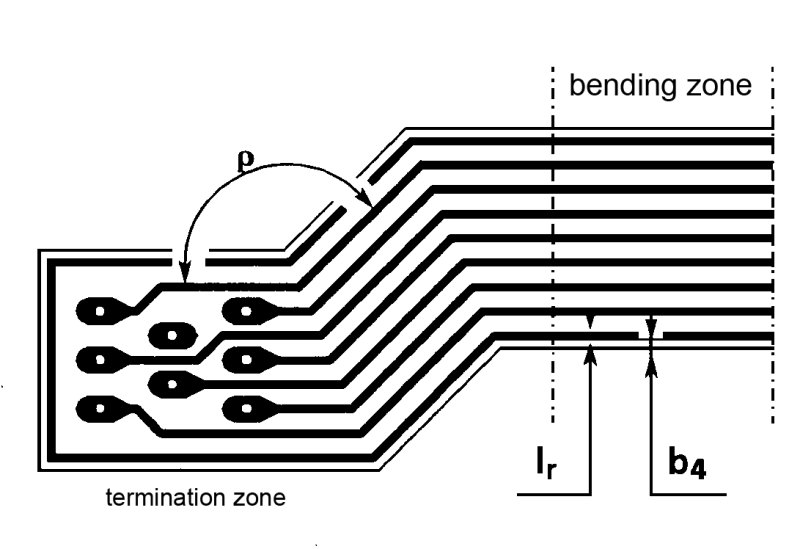 Figure 82: Tracks on flex, defining termination and bending zones.
Through holes
Annular ring
Annular ring on a flex PCB shall be the distance of the surface copper from the hole wall to the clearance opening in the cover layer.
Adhesive protruding from underneath the cover layer onto the surface copper shall be subtracted from the annular ring measurement.
Annular ring as-manufactured on a component hole shall be ≥ 0,25 mm.
Annular ring as-manufactured on non-soldering hole shall be ≥ 0,1 mm.
Vias and pads
PTH shall be located only in termination zones, not in the bending zone, as specified in Figure 82.
Terminal pads shall include PTH.
Terminal pads on single sided board have risk to be damaged during assembly. Terminal pads need to be reinforced by plating.
The cover layer shall include a clearance for assembly of a PTH in conformance with the clause 8.5.1.
Tear drop pad for flex PCB
The diameter of a circular pad with or without teardrop reinforcement shall be D1 as specified in Figure 83.
The diameter of an oblong pad shall be equal to D2 as specified in Figure 83.
The track width should be at least half the diameter of the pad except the case specified in the requirement 8.5.3d.
In the Figure 83 IC is track width and D1, D2 are diameters of the pad.
The track width may be less than half of the diameter of the pad in case the following conditions are met:
- a teardrop reinforcement is added to the connection of the track to the pad, and
- the reinforced zone has a length ≥ 0,8x the diameter of the pad.
In Figure 83 Zr is the length of the reinforced zone.
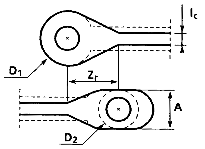 Figure 83: Teardrop reinforcement of terminal pads in flex PCB.
Bending radius
Overview
The PCB is designed to bend in L, U or S shapes with a radius of flexion that enables the PCB to be mounted and dismounted without damage. These radii depend on the type of board, the thickness of laminate and copper layers and a static or dynamic bending application, see Figure 84.
General
The radius on a flex PCB having 50 µm laminate thickness and 35 µm double sided copper thickness and including cover layer shall be ≥ 12x total thickness of the flex for a static application.
In the Figure 84 R is the bending radius of a flex PCB
Other PCB build-ups or dynamic applications shall be qualified by the supplier.
Other PCB build-ups include thicker laminate, thicker copper, or multilayers
The termination zone shall include all termination pads.
Bending of the flex PCB shall be designed not to occur on the termination zone and on an additional distance of 2 mm.
- 1 In the Figure 84 the additional distance is indicated as X.
- 2 Even though no bending is designed to occur on the termination zone, some bending can still occur on the assembled PCB due to the stress on the flex section. A stiffening of the termination zone by implementing double cover layer or adhesive can decrease the bending locally.
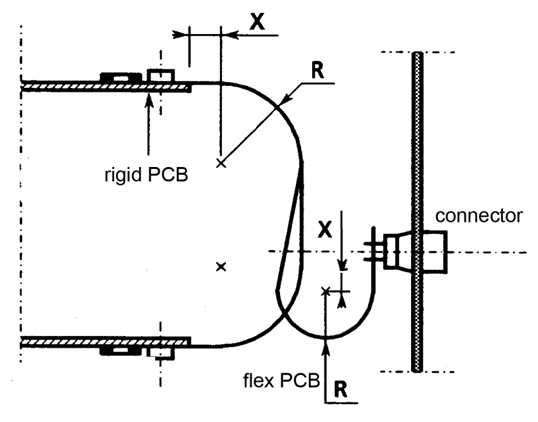 Figure 84: Bending radius of assembled flex
Sculptured flex PCB
Overview
Sculptured flex PCBs can be used as a connection between 2 PCBs or connectors. Sculptured flex circuits comprises of a copper circuit with different thickness sandwiched between two cover layers, as illustrated in Figure 85 and Figure 86.
General
The thickness of the cover layer, excluding adhesive, shall be 25 µm.
The thickness of the acrylic adhesive of the cover layer shall be 50 µm or 75 µm.
A typical cover layer is type Pyralux LF 0210 from DuPont.
The surface finish shall be in conformance with the requirement 7.8.1b.
- 1 This requirement specifies the use of hot oil reflowed tin-lead.
- 2 The connector pins are cut after reflow and exposed copper is permitted.
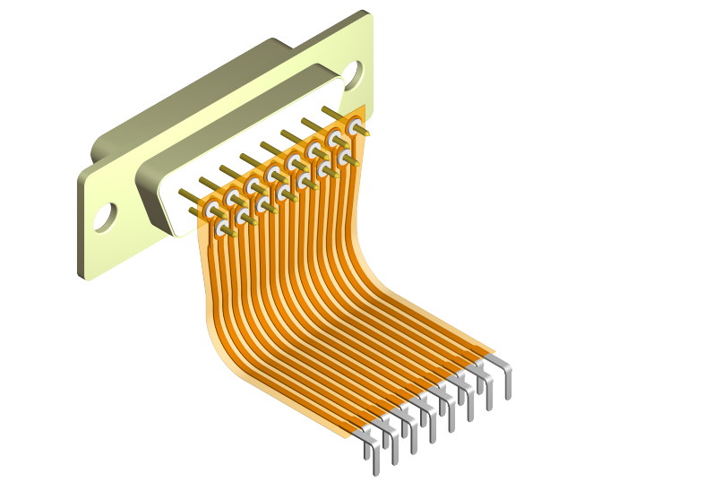 Figure 85: Sculptured flex circuit
Copper foil dimensions for build-up
A single foil of copper shall be used in the build-up.
Copper clad laminate is not used.
The initial thickness of the copper foil shall be 250 µm or 300 µm.
Copper type CW004 grade R240 ( ½ hard )
The sculptured shape of the copper shall be manufactured by selective etching of the copper foil.
The build-up, initial and etched copper thickness, track width and insulation distance shall be in conformance with the minimum dimensions specified in Table 81.
Table 81: Minimum as-manufactured dimensions of sculptured flex conductor
|
|
Thick initial copper
|
Thin initial copper
| ||
|
initial copper
|
etched copper
|
initial copper
|
etched copper
| |
|
Initial copper thickness
|
300 µm
|
|
250 µm
|
|
|
Track width for initial copper
|
400 µm
|
300 µm
| ||
|
Insulation distance for initial copper
|
500 µm
|
400 µm
| ||
|
Connection finger width
|
500 µm
|
350 µm
| ||
|
Etched thickness
|
|
150 µm
|
|
100 µm
|
|
Track width for etched copper
|
300 µm
|
200 µm
| ||
|
Insulation distance for etched copper
|
350 µm
|
250 µm
| ||
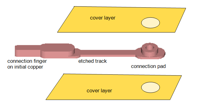 Figure 86: Build-up of sculptured flex circuit
Connection finger
The connection fingers may be bend in a staggered pattern to fit the footprint of the connecting PCB
An example of staggered bend connection fingers is shown in Figure 87.
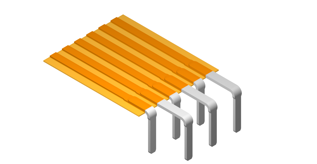 Figure 87: Connection finger of sculptured flex circuit
Through-holes
Through-holes shall be manufactured by drilling into the initial copper thickness.
Oblong pads should be used only in case circular pads cannot be used due to insufficient spacing in one direction.
The drill diameter of the hole shall be ≥ 0,5 mm.
Component holes with circular pads should have a pad diameter as-designed of ≥ 0,4 mm larger than the drilled diameter.
This results in a pad size of 200 µm as-designed.
The minimum as-manufactured pad size on the component side may be 0.
The pad size is similar to annular ring but this term is not used for sculptured flex technology. The as-manufactured pad size with misregistration is indicated with the red arrow in Figure 88.
There shall be no adhesive inside the hole.
Adhesive can be squeezed from underneath the cover layer and misregistration of the cover layer on component side can risk to have adhesive inside the hole.
The minimum as-designed pad diameter on the solder side should be ≥ 0,7 mm larger than the drilled diameter.
The annular ring on solder side shall be in compliance with the requirement 7.5.2c.
- 1 Requirement 7.5.2c specifies 200 µm.
- 2 The pad diameter on solder side is indicated with the blue arrow in Figure 88.
 Figure 88 Side view of a component hole for sculptured flex
Bending radius
The bending radius of sculptured flex circuit shall be ≥ 12x thickness and ≥ 3,2 mm.
Bending shall only occur on the etched track.
Bending shall not occur on the full thickness copper.
The etched track is shown in Figure 86 and copper thickness is specified in Table 81.
Rigid-flex PCBs
Overview
Multiple flex laminates with cover layers can be incorporated within a PCB. Figure 91 shows an example of 1 flex laminate incorporated in the rigid-flex PCB.
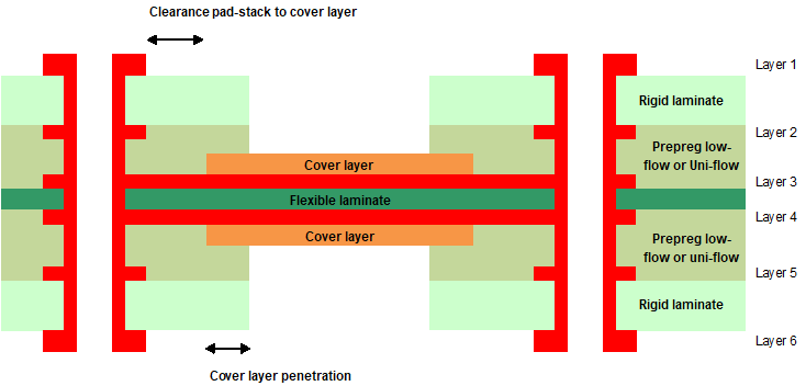 Figure 91 Example of a build-up of a 6 layer symmetric rigid-flex
General
The design of rigid parts of a rigid-flex PCBs shall be performed in conformance with the requirements from the clause 7.
The design of flex parts of a rigid-flex PCBs shall be performed in conformance with the requirements from the clause 8.
Design of rigid and flex parts include track width and spacing.
No termination zone shall be defined for the flex section of a rigid-flex PCB.
Build-up
The symmetry of the build-up shall be in conformance with the requirement 7.1.1a and 7.1.1b.
In the rigid part of the PCB the flex layers shall be bonded by using prepreg.
In the rigid part of the PCB adhesive shall not be used for bonding of the flex layers.
There are different manufacturing principles that either use standard flow prepreg as used in rigid boards, or modified no-flow type prepregs. No-flow prepreg cannot be used for resin filling of blind vias, and thereby a mix of prepreg styles can be necessary, when a sequential rigid-flex board is designed.
Copper foil thickness of 70 µm shall not be used on flex or rigid layers bonded with no-flow prepreg unless it is recorded as a Review Item in the PCB definition dossier.
This can add risk for bonding in cover layer bond cycles or the bond cycle with no-flow prepreg.
The number of flex laminates shall be ≤ 6, which can result in 12 copper layers when double sided flex laminates are used.
Flex layers can be bonded together by using a bondply cover layer with adhesive on both sides. The advantage of this is improved cleanliness between layers and improved control of impedance. The disadvantage is the flexibility and bending radius of the flex stack.
Three flex laminates or more in the build-up shall be recorded as Review Item in the PCB definition dossier.
Three flex laminates can include 6 copper layers.
Except the cases specified in the requirement 9.3h the rigid-flex PCB shall be designed and delivered with a support frame.
The rigid-flex PCB may be delivered without a support frame in case the following conditions are met:
- the PCB manufacturer delivers the rigid-flex PCB with a support that prevents damage to the PCB during shipment, and
- the customer implements a support structure that prevents damage to the rigid-flex PCB during assembly and handling.
Cover layer
The cover layer shall be placed in the flexible section of the PCB.
The cover layer shall not be placed in the rigid section of the PCB, except for the interface to the flex section as specified in the requirement 9.4c.
The cover layer shall extend into the rigid section of the PCB by ≥ 1,5 mm.
In a multilayer rigid-flex PCB where flex laminates are bonded together with bondply, the ends of the cover layers and bondply should be off-set in the rigid section by 1 mm to prevent a line of weakness.
The cover layer shall not overlap the internal pad of a via in the rigid section.
This is done to reduce stress on the hole wall due to high Z-expansion of cover layer adhesive and to maintain a good hole quality by not using dissimilar materials.
Interface of rigid part and flexible part
The hole wall shall be ≥ 2 mm separated from the edge of the rigid part of the PCB.
A larger separation between hole wall and edge of the rigid part is recommended in case it fits within the PCB lay-out.
Tracks on flex layers shall not change direction within 1 mm on both sides of the interface between flex and rigid sections.
Tracks extend 1 mm out of the rigid part of the PCB before they change direction. Tracks extend 1 mm into the rigid part of the PCB before they change direction.
Bending of the flex section shall be performed in conformance with the requirements from the clause 8.6.
Bending of the flex PCB shall not occur within 1,5 mm from the rigid section of the PCB.
Pads
The diameter of the pads on flex layers in the rigid section of the PCB shall be ≥ 0,6 mm larger than the diameter of the drilled hole except the case specified in the requirements 9.6b.
The diameter of pads on flex layers in the rigid section of the PCB may be < 0,6 mm larger than the diameter of the drilled hole in case the following conditions are met:
- the annular ring as-manufactured is achieved in conformance with requirements from the clause 7.3.4.3.3 of ECSS-Q-ST-70-10, and
- it is recorded as a Review Item in the PCB definition dossier. Non-functional pads on flex laminate shall be in conformance with requirement 7.5.1c.2.
Thermal rules and heat sinks
Overview
Heat sinks have the purpose of improving the thermal management of the PCB especially in the vicinity of components with a high thermal dissipation or current carrying tracks. Heat sinks also have an effect on in-plane thermal expansion.
Metal inserts, such as invar or molybdenum, can also be used to restrict in plane thermal expansion under large leadless components, such as LCC and AAD. Metal inserts are considered as heat sinks and are covered by this clause.
Heat sinks can affect the solderability of the PCB as they increase the thermal mass.
General requirements
Design with heat sink shall be recorded as a Review Item in the PCB definition dossier.
Heat sinks shall be electrically connected in conformance with the requirement 13.5a.
Specific requirements for external heat sink
Overview
Heat sinks can be smaller, larger or the same size as the PCB.
Construction of the interface between PCB and heat sink
Heat sink shall be made of copper or aluminium core bonded to the outer layer of PCB.
Bonding can be done by no-flow prepreg, cover layer or adhesive.
The copper or aluminium core shall have a protective layer to prevent corrosion.
The type of protective layer is specified in the PCB definition dossier. Examples of protective layers to prevent corrosion are anodization, alodine, nickel plating, gold plating. These corrosion protections can have specific drawbacks for further PCB processing.
The heat sink shall be manufactured by milling or etching.
Milling is preferred because it can provide better edge definition. Etching of thick layers result in a wider edge profile.
The PCB manufacturer shall inform the supplier of the method of bonding the heat sink.
This is done to verify the thermal properties of the assembly.
Minimum two non-plated through-holes shall be diagonally placed on the PCB for registration of the heat sink.
No conductive surface pattern shall be present beneath the heat sink, except the case specified in the requirement 10.3.2g.
A conductive surface pattern may be present beneath the heat sink in case:
- the adhesion of the heat sink to the external layer is ensured,
- the insulation of tracks of different potential is ensured,
- the surface area of tin-lead under the heat sink is minimised, and
- it is recorded as a Review Item in the PCB definition dossier.
- 1 For conditions specified in the requirements 10.3.2g.1 and 10.3.2g.3 to ensure adhesion on conductive surface pattern and tin-lead, it is an option to bond a cover layer on tin-lead or to perform selective stripping of tin-lead and bond with prepreg.
- 2 For condition specified in the requirement 10.3.2g.2 to ensure insulation, it is an option to bond a cover layer on conductive surface pattern.
- 3 The behaviour of tin-lead on a PTH pad during assembly can affect the design of the bonding method of the heat sink.
Dimensional requirements
The mechanical stability of individual clearances of the pattern of the heat sink shall be recorded as a Review Item in the PCB definition dossier.
Distance between 2 clearances shall be ≥ 1,5 mm along straight edges.
Distance along straight edges is indicated as “Iz1” in Figure 101.
The length of the straight edges shall be reviewed for mechanical stability in conformance with requirement 10.2a.
Distance between 2 clearances shall be ≥ 1,0 mm between circular edges.
Distance between circular edges is indicated as “Iz2” in Figure 101.
Distance between pads on the PCB and the edge of the clearance of the heat sink shall be ≥ 0,3 mm.
Distance between pads on the PCB and the edge of the clearance of the heat sink is indicated as “i” in Figure 101.
Distance between a clearance in the heat sink and the edge of the PCB laminate shall be ≥ 0,5 mm.
Distance between a clearance in the heat sink and the edge of the PCB laminate is indicated as“b6” in Figure 101.
Distance between the clearance in the heat sink and the edge of the heat sink shall be ≥ 1,5 mm.
Distance between the clearance in the heat sink and the edge of the heat sink is indicated as“b7” in Figure 101.
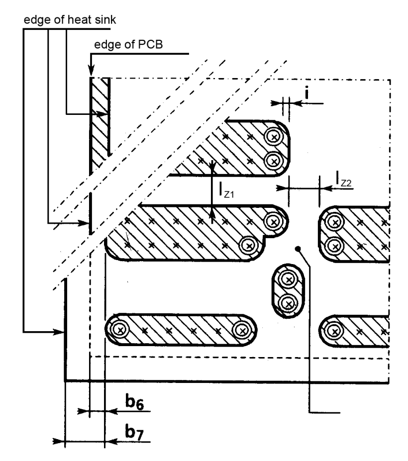 Figure 101: Lay out of heat sink and PCB
Specific requirements for internal heat sink
General
Heat sink shall be made of copper, copper-molybdenum-copper or CIC.
- 1 Heat sinks can be foils covering the entire surface of a layer or inserts placed locally under a specific component.
- 2 Heat sinks that consist of a copper layer can be made by using copper foil or copper clad laminate. The advantage of a foil is the ability of prepreg to fill clearances from both sides. The advantages of copper clad laminate is better registration, ease in handling and processing and the possibility of more complex electrical routing in case of split ground planes on heat sinks.
There should be no tracks on the same layer as a heat sink.
Local heat sink inserts can have tracks on the same layer.
Cu thickness and type
Foils and laminates with as-designed copper thickness ≥ 105 µm shall be designed in conformance with the requirements from clause 10 for heat sinks.
The number of copper heat sink layers shall be ≤ 2.
The thickness of copper layer shall be 105 µm to 210 µm in case 2 layers of heat sinks are used.
The thickness of copper heat sink shall be ≤ 700 µm when 1 layer of heat sink is used.
The copper foil shall be procured in conformance with the requirements from the IPC-4562.
Types of copper foil types commonly used are: HTE grade 3, and JTC grade 1.
Copper foil for heat sinks shall be in conformance with the requirement 7.1.2i.
High quality copper foil type HTE or JTC is necessary to ensure reliable electrical connection with vias.
CIC and Molybdenum inserts
CIC may be used to reduce in plane CTE.
- 1 Material designation IPC-CF-152/2 CIC W 6D as specified in IPC-CF-152B.
- 2 Most common composition of CIC is 12,5% copper, 75% invar, 12,5% copper.
The thickness of CIC shall be ≤ 150 µm.
The number of heat sink layers with CIC shall be ≤ 2.
The CIC layers shall have a tolerance of ≤ ± 10%.
Molybdenum may be used to reduce in plane CTE and improve heat transfer.
Standard specification for molybdenum is according to ASTM-B386-03.
The thickness of molybdenum inserts shall be 0,5 mm.
The number of layers containing molybdenum inserts shall be ≤ 1.
The molybdenum inserts shall have a tolerance of ≤ ± 0,035 mm.
Dimensional requirements
The mechanical stability of individual clearances of the pattern of the heat sink shall be recorded as a Review Item in the PCB definition dossier.
Clearances that are separated by a long straight edge known as ‘thin web’ are a concern for mechanical stability.
For heat sinks that are designed to be within the edge of the PCB, the distance between the edge of the heat sink and the edge of the PCB shall be ≥ 1,5 mm.
Sufficient resin from the edge of the heat sink to the edge of the PCB ensures adequate insulation and mechanical stiffness needed for subsequent milling of the PCB.
Heat sinks that are aligned with the edge of the PCB or exposed on one side by depth controlled milling shall have a protective coating for corrosion protection.
Example of protective coating is nickel plating.
The distance between a plated hole and the heat sink shall be in conformance with the requirement 13.8.2k and values specified in the Table 133.
The distance between two circular clearances shall be ≥ 2x the copper thickness of the heat sink.
In case the distance between the two clearances is less than two times the copper thickness, the remaining metal shall be removed.
This remaining metal is named “thin web”. This is illustrated in Figure 102.
In case holes are overlapping, the angle of intersection, as specified in Figure 103, shall be minimum 110°.
This applies to etching as well as drilling and milling.
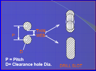 Figure 102: drilling holes and slots in internal heat sink
 Figure 103: Angle of intersection of overlapping holes
HDI PCBs
Overview
This clause defines additional technology for HDI PCBs, such as microvias. In addition, this clause specifies deviations for the following features:
For dielectric thickness of microvia layers on HDI PCBs, a deviation to requirement 7.1.3e is specified in requirement 11.4.1h.
For copper foil thickness on microvia layers on HDI PCBS, a deviation to requirement 7.1.2c is specified in requirement 11.4.1e.
For fine pitch track width and spacing of impedance controlled routing to 1 mm pitch AAD on HDI PCBs, a deviation to requirement 7.4.5a is specified in requirement 11.5.5a.
For annular ring of internal pads for fine pitch footprint on HDI PCBs a deviation to requirement 7.5.2a is specified in requirement 11.5.2a.
For aspect ratio of 1 mm pitch AAD on HDI PCBs, a deviation to requirement 7.3.5a is specified in requirement 11.5.6a.
Justification
A PCB may be classified as HDI PCB during the design review in case the routing cannot be performed using conventional dimensions due to the assembly of high I/O components.
An HDI PCB shall be designed in conformance with the requirements of the clause 11.
All design features of the clause 11 shall be recorded as a Review Item in the PCB definition dossier.
Microvia technology
For the design of an HDI PCB the following technologies shall apply:
- without microvias,
- with microvia staggered with buried via without cap,
- with microvia stacked on cap plated filled buried via.
- 1 HDI technology without microvias as specified in requirement 11.3a.1 is typically of lower complexity and of higher reliability compared to HDI technologies with microvias. HDI technology with staggered microvias as specified in requirement 11.3a.2 is of lower complexity compared to stacked microvias as specified in requirement 11.3a.3. It is recommended to design using less complex technology.
- 2 Examples of stacked and staggered microvias in the build-up of an HDI PCB are shown in Figure 111. The offset achieved by staggering is indicated as D.
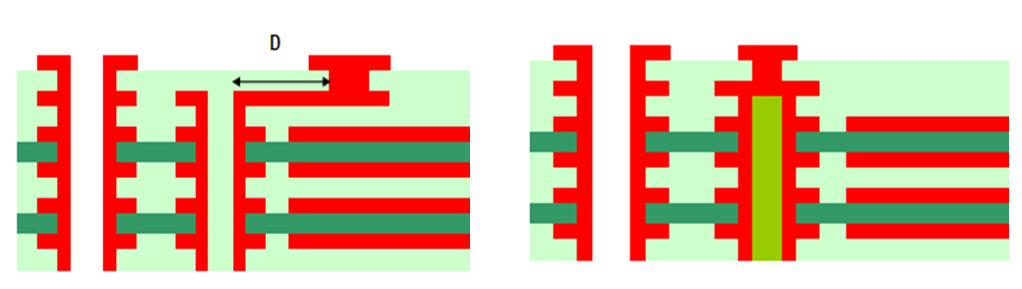 Figure 111: Build-up of HDI PCBs with staggered (left) and stacked (right) microvia.
Microvias
Build-up of microvia layers
In case microvias are used, they shall connect from an external layers of the rigid section of the PCB.
In case microvias are used, the number of microvia layers on either side of the core PCB shall be 1.
Dummy copper plane filling should be used on internal microvia layers.
Dummy copper is used to establish a lay-out that is as homogeneous as possible. This is done to reduce embedding of copper circuit into the resin and to maximise the dielectric thickness.
On microvia layers, the external and internal copper layers should be designed using basic copper thickness 17 µm.
On microvia layers, the external and internal copper layers may be designed using basic copper thickness of 9 or 12 µm, in case the following conditions are met:
- the peel strength is measured on the test coupon to be ≥ 12 N/cm,
- a carrier on the foil is used during manufacturing, and
- it is recorded as a Review Item in the PCB definition dossier.
- 1 The copper thickness defined in requirement 11.4.1d is in conformance with the requirement 7.1.2c. The copper thickness defined in requirement 11.4.1e is a deviation from the requirement 7.1.2c.
- 2 The benefit of reduced copper thickness is to improve etching accuracy of fine features. To ensure an insulation of 60 µm between layers it can be beneficial to use thin copper on the internal microvia layer to avoid planarization processes.
- 3 The potential lower peel strength of thin copper foil is a risk factor for manufacture, which is mitigated by the coupon measurement.
- 4 Thin copper foil is more fragile, therefore a rigid carrier is used during manufacture. When the core surface is non-planar, it is possible the rigid carrier does not conform well to the non-planar prepreg causing lack of adhesion or deformation of the copper foil. The following features can cause non-planarity of the core surface: rigid-flex constructions, high via density, high track density, high copper thickness, use of no-flow prepreg.
Microvia layers should be designed with copper foil and prepreg.
Insulation of microvia layers shall be performed by using 2 sheets of prepreg in conformance with the requirement 7.1.3a.
The as-manufactured insulation in Z direction in microvia layers shall be ≥ 60 µm in conformance with Table 133.
This is a deviation from the requirement of 70 µm as specified by the requirement 9.6.c.6 of ECSS-Q-ST-70-10.
The as-designed insulation in Z direction in microvia layers shall be ≤100 µm.
The typical configuration to achieve ≥60 µm and ≤100 µm insulation, is by using 2 sheets of prepreg type 106.
For voltages >30V microvia layers shall not have superimposed conductors.
This is done to ensure that insulation in Z direction is in conformance with the Table 133.
Design of microvias
The aspect ratio of a microvia on a HDI PCB shall be ≤ 1.
The microvia shall be laser drilled.
The microvia shall be filled with copper.
The dimple on the surface of the filled microvia shall be ≤ 30 µm.
An illustration of a dimple on a microvia is given in Figure 112.
The plated copper thickness on the corner of the microvia shall be ≥25 µm.
Microvia diameter should be ≥ 150 µm as-designed.
The tolerance is small therefore the diameter as-manufactured is approximately identical.
The diameter of the area connecting to layer 2 shall be ≥ 100 µm as-manufactured.
This is less than 150 µm as-designed to allow for conical shape of microvia.
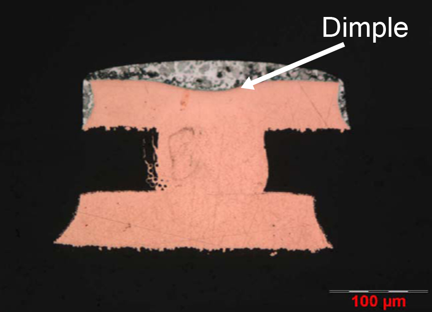 Figure 112: Dimple on a microvia
Pad design for microvia
The diameter of external pads shall be the diameter of the ablated hole plus ≥ 0,15 mm.
The diameter of external pad may be the diameter of the ablated hole plus ≥ 0,1 mm in case the following conditions are met:
- the annular ring is in conformance with the requirement 11.4.4b, and
- the diameter of external pad is recorded as a Review Item in the PCB definition dossier. The diameter of internal pads shall be the diameter of the ablated hole plus ≥ 0,15 mm.
It is important to consider the complexity of the PCB and the PCB manufacturing tolerances for the design of the diameter of the pads.
The internal pad of a staggered microvia and the pad of the buried via may be placed tangent to each other.
Assuming 100 µm and 10 µm for the annular ring as-manufactured of the pads of blind via and microvia, this results in a distance of about 110 µm.
Annular ring for microvias
The annular ring as-manufactured for microvias for internal pads shall be ≥ 10 µm.
The annular ring as-manufactured for microvias on external layer shall be ≥ 10 µm
The visual inspection on external layer possible on all microvias can use as criteria no breakout, i.e. tangency. This is done because it is not possible to visually inspect for this annular ring requirement.
Evaluation of annular ring of microvias by microsectioning shall be in conformance with the requirement 11.4.4b.
Core PCB for HDI
General build-up
For HDI PCB, the core PCB shall be type rigid or rigid-flex.
The rigid part of an HDI PCB shall be designed in conformance with the requirements from the clause 7.
The total number of copper layers in the rigid part shall be in conformance with the requirements from clause 7.3.4.
The total number of copper layers include the microvia layers.
PCB thickness shall be in conformance with the requirements from the clause 7.3.
Copper thickness of internal layers that do not include microvias shall be in conformance with the requirement 7.1.2a.
Annular ring on vias for fine pitch footprint
The diameter of internal pads may be reduced in case the following conditions are met:
- a teardrop reinforcement is implemented,
- the annular ring as-manufactured in the direction of the track is in conformance with the requirement 7.5.2a,
- the annular ring as-manufactured in the directions that are opposite and perpendicular to the track are > 25 µm,
- length of wicking and drilling cracks is ≤ 25 µm, and
- it is recorded as a Review Item in the PCB definition dossier.
- 1 Requirement 7.5.2a specifies annular ring >50 µm.
- 2 Requirement 11.5.2a.3 is a deviation of the requirement for annular ring 7.5.2a.
- 3 In the requirement 11.5.2a.4 length of wicking and drilling cracks is the same dimension as the annular ring. This permits less wicking and drilling cracks than the requirement 7.3.4.3.3.e.1 of ECSS-Q-ST-70-10.
- 4 An example of teardrop pad design is shown in Figure 113. In this figure “A” is the minimum annular ring between hole and circular pad design; “B” is the effective annular ring with teardrop reinforcement applied.
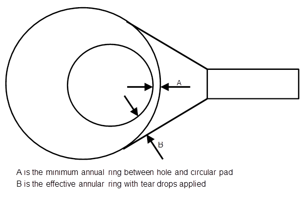 Figure 113: Tear drop pad design
Track width and spacing on external layers
External layers should not include tracks.
This is in particular important for critical tracks.
The spacing and width of pads and tracks for external layers may be reduced to requirements for fine pitch in conformance with the values specified in Table 74.
The length of fine pitch on external layers shall be in conformance with the requirement 7.4.3g.
Track width and spacing on internal layers for impedance control and routing to AAD
The spacing and width of pads and tracks for impedance control and routing to AAD on internal layers may be reduced to requirements for fine pitch in conformance with the values from Table 75.
The requirements for fine pitch of clause 7.4.5 shall apply.
An example of routing a differential pair in a 1,27 mm pitch footprint is given in Figure 114. Ground planes on other layers are omitted for clarity. The following dimensions are considered:
- The available pad diameter is 710 μm.
- Allowance for design router is 10 μm.
- The maximum pad diameter is 700 μm.
- The minimum annular ring as-designed is 150 μm.
- Pad design includes teardrop and minimum annular ring as-manufactured as defined in requirement 11.5.2a.
- The maximum available drill diameter is 400 μm.
- The maximum aspect ratio is 7.
- The maximum board thickness for the drill sequence is 2,8 mm.
 Figure 114: Example of routing two differential pair tracks between vias in a footprint of an AAD with 1,27 mm pitch.
Track width and spacing on internal layers for differential pair routing within the footprint of 1,0 mm pitch AAD
On internal layers the width of tracks may be reduced to 80 µm and the spacing reduced to 90 µm, in case:
- the tracks route an edge-coupled differential pair between via pads for a 1 mm pitch AAD,
- the current is ≤ 50 mA and voltage is ≤ 10 V,
- the spacing and track width are increased outside the footprint of the AAD to normal values in conformance with the requirements from clause 7.4.6,
- the copper thickness is in conformance with the requirement 7.4.5g,
- the manufacturing tolerance for 90 µm spacing is within -10% / +20%,
- the manufacture of the tracks is inspected prior to lamination for conformance with designed track width and spacing within the required tolerance, and
- it is recorded as a Review Item in the PCB definition dossier.
- 1 NOTE to 11.5.5a.5: This reduces the tolerances from the standard ±20% as specified in the Table 73. This provides a minimum as-manufactured insulation distance of 81 µm as specified in the Table 133.
- 2 NOTE to 11.5.5a.6: The inspection can be performed by AOI and by dimensional measurement under microscope on the foot of the track for spacing and track width.
- 3 The reduced feature sizes increase the risk of errors during etching resulting in open or short circuits.
Aspect ratio of vias for footprint of AAD with 1 mm pitch
The aspect ratio of vias may be higher than 7 as specified in the requirement 7.3.5a in case:
- the aspect ratio is ≤ 10,
- the vias are used within the footprint of an AAD with a pitch of 1mm,
- the plating inside vias with high aspect ratio is verified on the coupon as specified in the requirement 15.2d.6, and
- it is recorded as a Review Item in the PCB definition dossier.
- 1 It is more difficult to achieve homogeneous plating and the required thickness inside vias with a high aspect ratio.
- 2 An example of routing a differential pair in a 1 mm pitch footprint is given in Figure 115. Ground planes on other layers are omitted for clarity. The following dimensions are considered:
- The available pad diameter is 570 μm.
- Allowance for design router is 10 μm.
- The maximum pad diameter is 560 μm.
- The minimum annular ring as-designed is 150 μm.
- Pad design includes teardrop and minimum annular ring as-manufactured is as defined in requirement 11.5.2a.
- The maximum available drill diameter is 250μm.
- The maximum aspect ratio is 10.
- The maximum board thickness for the drill sequence is 2,5 mm.
 Figure 115: Example of routing two differential pair tracks between vias in a footprint of an AAD with 1 mm pitch.
PCBs for high frequency applications
Material selection
Table 61 presents examples of some materials used for manufacture of RF PCBs. For the selection of materials it is important to consider that materials with good RF performance typically have poorer processing characteristics (e.g. adhesion and resin flow during lamination). High performance RF materials can exhibit lower peel strength of copper. This can affect the assembly. Some RF materials based on PTFE or mixed build-ups can exhibit smear in the drilling process. For material selection it is important to consider the RF properties and the processability of the material. The possibility to mix for instance RF laminate with standard prepreg can provide good processability while maintaining acceptable RF performance.
Build-up of RF PCB
The build-up of RF PCBs shall be in conformance with requirements from clause 7.1, except the cases specified in the requirements from 12.2b to 12.2e.
For copper cladding and copper foils the requirements 7.1.2h, 7.1.2i shall not apply.
Copper type “electrodeposited - ED” or “rolled and annealed - RA” may be used for copper cladding and copper foils.
For Molybdenum and CIC layers the requirement 7.1.1c shall not apply.
Molybdenum and CIC layers shall not be used in RF PCBs.
Embedded film resistors
The use of embedded film resistors in internal layers shall be recorded as a Review Item in the PCB definition dossier.
The tolerance on the as-manufactured resistance value shall be ≤ ±20%.
Due to the relatively high tolerance, the application of embedded film resistors is limited to line termination.
Embedded film resistors shall be of type NiP or NiCr.
Type NiP is available from OhmegaPly. Type NiCr is available from Ticer.
A surface resistance of 25 Ω/sq should be used.
A surface resistance of 50 Ω/sq may be used.
A surface resistance of 25 Ω/sq is achieved on a thicker resistive layer which is beneficial for thermal reliability.
Layers that include embedded film resistors should not be plated.
This is done to achieve the best accuracy of etching and resistor value as-manufactured.
No more than one plating sequence shall be performed on layers that include embedded film resistors.
All embedded film resistors on a layer should be oriented in a single direction.
The orientation of embedded film resistors shall be recorded as a Review Item in the PCB definition dossier.
The best etching accuracy is obtained when embedded film resistors are oriented in the direction of the conveyor of the etching process.
The width of an embedded film resistor shall be ≥ 250 µm.
The aspect ratio of length and width of an embedded film resistor shall be ≥ 1.
A higher aspect ratio achieves better accuracy of the resistive value.
The ratio of length to width of an embedded film resistor shall be ≤ 5.
- 1 A lower ratio achieves better thermal endurance.
- 2 The configurations specified in requirements 12.3d, 12.3e, 12.3k and 12.3l provide embedded film resistor values between 25 Ω and 250 Ω.
Dedicated representative coupons shall be designed to allow verification of the embedded film resistor values on the etched layer before further lamination.
Dedicated representative coupons shall be designed to allow verification of the embedded film resistor values on the as-manufactured PCB as specified in the requirement 15.2d.13.
Thickness of RF PCB
The thickness of RF PCB as-designed should be ≤ 3 mm.
The thickness of RF PCB as-designed may be > 3 mm in case the following conditions are met:
- the thickness as-designed is ≤ 5,5 mm,
- the materials used are not based on PTFE, and
- it is recorded as a Review Item in the PCB definition dossier.
High PCB thickness involve a more difficult drilling process, lamination and handling in automated equipment. It is important that the PCB manufacturer confirms the good processability of the materials.
The number of layers for RF PCBs should be ≤ 8.
The number of layers for RF PCBs may be > 8 in case the following conditions are met:
- the number of layers is ≤ 14, and
- it is recorded as a Review Item in the PCB definition dossier.
Track width and spacing
External layers
The spacing and width for external layers of RF PCBs shall be in conformance with the values from Table 74.
For RF elements the spacing may be reduced to the values in conformance with Table 121 in case:
- the voltage between nets is ≤ 1 V,
- no assembly is performed on the RF elements,
- no critical tracks are included in the RF element,
- a specific visual inspection and functional measurement of the RF element is performed, and.
- it is recorded as a Review Item in the PCB definition dossier. Table 121: Minimum spacing and width as-designed for RF elements on external layers
|
Total copper thickness (base + plated) [µm]
|
17,5≤Th≤50
|
Th>50
|
|
width [µm]
|
125
|
200
|
|
spacing [µm]
|
125
|
200
|
Internal Layers
The spacing and width for internal layers of RF PCBs shall be in conformance with the values from Table 75.
Pad design
Pad dimensions
Dimensions of the via hole pads shall be in conformance with the requirements from clause 7.5.2.
Non-functional pads
Removal of non-functional pads shall be performed in conformance with the requirements from clause 7.5.1.
Surface finish
The surface finish for RF PCBs shall be in conformance with the requirements from clause 7.8.1.
Profiled layers and vias
Z-controlled backdrilling of vias may be used in case:
- the Z-controlled backdrilling on vias is included on the coupon, and
- it is recorded as Review Item in the PCB definition dossier.
Backdrilling is done to achieve better insulation or to avoid antenna effect of the via wall.
The use of profiled top layers shall be recorded as a Review Item in the PCB definition dossier.
Profiled layers can be manufactured by Z-controlled milling or by laminating layers with openings. Profiled top layers can be used to expose a signal circuit on layer 2 in case the top layer is used as ground plane.
The use of profiled aluminium backing used for cooling shall be recorded as a Review Item in the PCB definition dossier.
Electrical requirements for PCB design
Overview
Table 131 explains the terms “AND”, “OR” and “FOR” as well as the used cross referencing to requirements or notes in Table 133, Table 134, Table 135, Table 136 and Table 137.
Table 131: Legend of terms
|
Terms
|
Meaning
|
|
AND
|
The term “AND” indicates that the largest value of the two are used for the relevant voltage.
|
|
OR
|
The term “OR” indicates that various options are listed and any of the options can be selected.
|
|
FOR
|
The term “FOR” indicates the perimeter of a technology (for example HDI, fine pitch, uncoated connectors) for which an exemption has been specified to a requirement for standard insulation distance.
|
|
Cross-reference to requirement
|
Cross-referencing to requirements is used to trace back the short descriptions given in the tables to the normative references.
|
|
Cross-reference to Note
|
Cross-referencing to notes is used to trace back the short descriptions given in the tables to informative references.
|
Figure 131 illustrates the insulation distances, numbered 1 to 5, specified in the Table 133, Table 134, Table 135, Table 136 and Table 137.
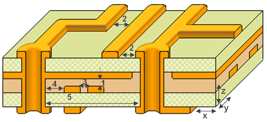 1: spacing in Z direction
2: spacing in X,Y direction on external layer
3: spacing in X,Y direction on internal layer between conductors
4: spacing in X,Y direction on internal layer between a conductor and a hole wall
5: spacing in X,Y direction on internal layer between hole walls
Figure 131: Cross section of PCB with insulation distances.
General
The term “AND” indicates that the largest value of the two shall be used.
This is explained in Table 131.
PCB drying
Precautions shall be taken to reduce the moisture level inside the PCB for electrical testing and for measuring electrical characteristics.
Recommended bake for bare PCB is 6 hours at 120˚C. Polyimide is more hygroscopic than epoxy.
Electrical characteristics
Insulation resistance between tracks shall be:
- intralayer: > 1010 Ω,
- interlayer: > 1011 Ω.
DWV between tracks shall be 1000 Vrms/mm for intralayer and interlayer.
Short-time current overload shall be in conformance with the requirements from the clause 7.3.5.1.2 of ECSS-Q-ST-70-10.
Long-time current overload shall be in conformance with the requirements from the clause 7.3.5.1.3 of ECSS-Q-ST-70-10.
The values for current overload from 7.3.5.1.2 and 7.3.5.1.3 of ECSS-Q-ST-70-10 are summarised in the Table 132.
Table 132: Current overload limits
|
Basic copper thickness
|
Short-time current overload
|
Long-time current overload
|
|
9 µm
|
n/a
|
n/a
|
|
17 µm
|
n/a
|
n/a
|
|
35 µm
|
7 A for 4 s
|
≥ 8 A
|
|
70 µm
|
14 A for 4 s
|
≥ 16 A
|
For power distribution a copper thickness of 35 µm or more should be used.
Thin copper tracks of below 35 µm are not suitable for power distribution. Therefore no requirement is specified for thin copper.
In case sequential lamination increases the copper thickness, the current limits may be interpolated or extrapolated.
Floating metal
All conductive parts and patterns shall not be left isolated, in conformance with clauses 6.3.1, 9.2.1 and 9.2.2 of ECSS-E-ST-20-06.
ECSS-E-ST-20-06 defines:
- the area of a floating surface is ≤ 1 cm2
- the capacitance of the floating surface is ≤10pF.
Current rating
Overview
Current rating in PCB tracks is based on the temperature increment of tracks compared to the initial PCB temperature when not powered. The method to compute the maximum allowed current is based on families of isothermal curves. These curves cover a range from 1°C up to 100°C and allow to compute the current starting from the copper cross section of the track or vice versa, for the required temperature increment.
The current rating model used in this standard is specified in the document IPC-2152 and the model is presented in graphical form. This standard is an evolution of and supersedes the previous model from IPC-2221A. Another model is presented in CNES/QFT/IN.0113, which is a more conservative model compared to IPC-2152. The mathematical fitting of the three models is presented as a guideline in Annex D. A comparison of the models is shown in Figure D-1.
Requirements for temperature increment
The temperature increment of tracks with respect to the dielectric substrate shall be ≤ 10 °C.
The temperature increment of tracks with respect to the dielectric substrate should be ≤ 5 °C.
The temperature of tracks shall be ≤ 95 °C.
The temperature of tracks should be ≤ 85 °C.
The increment of 10 °C is based on a temperature of the PCB substrate of 85 °C, in which case the tracks can heat to 95 °C due to self-heating. The self-heating of tracks up to 10°C compared to the substrate, regardless of overall substrate temperature, is based on heritage.
Requirements for the model IPC-2152 for current rating
Except for the cases specified in the clause 13.6.4, the model used to calculate temperature increment shall be in conformance with the model for conductor sizing in space environment in conformance with requirements specified in chapters 1 to 5 and appendix A of IPC-2152.
The mathematical fitting of Figure 5-14 of chapter 5.2.2. of IPC-2152 and the other models is presented as a guideline in Annex D.
Current rating shall apply to the conductive circuit of the as-manufactured PCB including manufacturing tolerances.
- 1 Minimum as-manufactured track width and minimum as-manufactured copper thickness include tolerances specified in Table 71 and Table 73.
- 2 The graphical representation of the model in IPC-2152 uses nominal dimensions for track width and copper thickness. Chapter A.4.3. of IPC-2152 specifies that the final cross sectional area can be significantly different from the nominal value and needs to be considered.
The PCB configuration for which IPC-2152 is used to calculate current rating, shall be as follows:
PCB thickness is more than 1,5 mm.
PCB dielectric material has a thermal conductivity as for polyimide or epoxy.
PCB total surface area is more than 75x75 mm.
In case the PCB configuration is not in conformance with requirement 13.6.3c, the supplier shall demonstrate the validity of the model used for the current rating.
In this case the model of IPC-2152 is not considered to be valid.
The temperature rise of a track may be reduced when it is superimposed by a copper plane, in conformance with requirements specified in chapter A.4.6.2. of IPC-2152.
This chapter specifies that the presence of copper planes is recommended to be used to calculate temperature and to be considered as design margin.
Current rating of a via shall use the same temperature rise as a track with equivalent cross section, in conformance with requirements specified in chapter A.3.4 of IPC-2152.
This chapter specifies that multiple vias can be used to reach the same cross sectional area of the connecting track.
Multiple tracks in parallel with a spacing of less than 25 mm shall be assessed as parallel conductors, in conformance with requirements specified in chapter A.3.3 of IPC-2152.
Temperature rise of parallel conductors is determined by calculating the equivalent cross-sectional area and the equivalent current. A summary is also given in paragraph “e” of chapter 4 of IPC-2152.
The current rating of polyimide and epoxy PCBs shall be in conformance with requirements specified in chapter A.4.4 of IPC-2152.
The chapter A.4.4 in IPC-2152 specifies that there is less than 2% difference.
Amendments to the model from IPC-2152
Overview
The requirements of the clause 13.6.4.2 specify amendments with respect to the model for conductor sizing in space environment defined in the clause 13.6.3. These amendments are specified for the current rating and for the temperature rise in the specified configurations.
List of amendments
The current rating of external conductors shall be reduced by 10%.
This is an amendment to chapter A.6 of IPC-2152, which specifies that the current rating of external layers is the same as for internal layers. The justification for the 10% margin is specified in chapter 4.5 of CNES/QFT/IN.0113.
For PCBs with a thickness between 1,5 mm and 1,8 mm, the temperature rise of tracks shall be increased by 20%.
The mathematical fitting of Figure 5-14 of chapter 5.2.2. of IPC-2152 presented as a guideline in Annex D is valid for PCBs of 1,8 mm. The justification for 20% margin for thinner PCBs is given in chapter A.4.2 of IPC-2152.
Current rating of a via connecting to a copper plane may be 5 times higher.
This amendment to IPC-2152 is based on chapter 5.3 of CNES/QFT/IN.0113.
Current rating of a track may be 5 times higher in case it is less than 2mm long and connecting a via to a copper plane.
This amendment to IPC-2152 is based on chapter 5.3 of CNES/QFT/IN.0113.
In case a track leads to a PTH of a connector footprint and the track is reduced in width to pass between pads within the footprint, the current rating may be 2 times higher.
This is specified to avoid reducing annular ring to allow a wider track to pass in between pads. The increased current rating is justified by the presence of PTHs with copper pads used for assembly of connectors.
Provisions to prevent open circuit failure on critical tracks
Overview
The open circuit failure of a track in a PCB can lead to loss of function, a random behaviour, or worse, to the propagation of failure. As example, the open circuit failure of a connection in the DC/DC converter feedback loop can cause the loss of the DC/DC function and the failure propagation to the supplied downstream circuits.
Routing
Criticality of tracks shall be as specified in requirement 13.9.2a.
Critical tracks should be routed on a single layer.
A verification shall be performed to reduce the use of vias on critical tracks.
Some automated routing software can cause unnecessary use of vias.
For a critical track a second redundant via shall be used for the interconnection.
This is done to prevent open circuit failure of a single interconnection between track, via pad and via barrel.
Voltage rating
Overview
The insulation distance is determined by the following parameters:
Voltage rating, as specified in requirements of clause 13.8 for single insulation and in clause 13.9 for double insulation.
Manufacturing tolerances associated with the copper thickness and track width, as specified in requirements of clause 7.4.1.
Manufacturing capability as function of copper thickness, as specified in requirements of clause 7.4.3 for external layers and requirements of clause 7.4.4 for internal layers.
Exemptions made to accommodate HDI designs, as specified in requirements 11.4.1h, 11.4.1i, 11.4.1j, 11.5.2a, 11.5.3b, 11.5.4a, 11.5.5a and 11.5.6a.
Exemptions made to accommodate the use of uncoated connectors, as specified in requirements of clause 13.8.4.
Tolerances on laminate or prepreg, as specified in requirements of clause 7.1.3.
Tolerances on hole wall to hole wall registration depending on number of bond sequences, as specified in requirement 13.8.2i and its Note.
All parameters listed are included in Table 137.
General requirements
Voltage rating shall apply to the as-manufactured PCB.
Voltage rating shall apply to the worst-case peak transient voltage.
The supplier shall design the PCB with the insulation distances as specified in the requirements from the clause 13.8.
The insulation distance as function of voltage of the as-manufactured PCB shall be in compliance with values specified in Table 133 and Table 134.
- 1 The insulation distances also depends on manufacturing capability and tolerances as specified in clause 13.8.1 and specified in Table 74 and Table 75.
- 2 The Table 133 and Table 134 cover any elevation. Withstanding voltage between two tracks in air at 87% relative humidity is 1600 V/mm. It is considered that breakdown or arcing cannot occur below this field strength as indicated in the paper by D. P Cullen and G O’Brien (see bibliography).
Insulation distance in Z direction for superimposed conductors shall be in conformance with values specified in Table 133 and Table 134.
The requirements 7.1.3e and 10.3.1 also specify insulation distance of superimposed conductors, as explained in the clause 13.8.1.
Conductors that are not superimposed in Z direction shall be offset in X,Y direction by the distance for X,Y internal conductor-to-conductor spacing as specified in Table 133 and Table 134.
Insulation distance from conductors to plated or non-plated hole wall shall be in conformance with the values specified in the Table 133.
These insulation distances include an additional spacing of 50 µm to allow for wicking. The requirement does not need to be considered in addition to the requirement for X,Y internal conductor-to-conductor spacing in case the minimum annular ring as-manufactured is 50 µm and the wicking is ≤ 50 µm.
Insulation distance of conductors to PCB edge shall be as for X,Y internal conductor to hole wall, as specified in Table 133.
The insulation distance between hole wall of vias on different nets shall be in conformance with the values specified in the Table 133.
The as-manufactured distance is not affected by the number of bond sequences. However, the tolerance on the as-designed distance increases with the number of bond sequences, as specified in the Table 137.
The insulation distance between hole wall of vias on the same net may be less than the distances specified in the Table 133.
Vias on the same net can be used for redundancy. This can apply in particular for microvias.
The insulation distance between the heat sink and a hole wall shall be in conformance with values from Table 133.
Voltages above 500 V shall be subject to specific qualifications of the design.
Table 133: Minimum insulation distance as function of voltage on as-manufactured PCB for rigid laminate.
|
V
|
Z
|
X,Y external with conformal coating
|
X,Y external without conformal coating
|
X,Y internal conductor to conductor
|
X,Y internal conductor to hole wall
|
X,Y internal
|
|
0-10V
|
70 µm
|
120 µm
|
200 µm
|
104 um
|
154 µm
|
350 µm
|
|
11-30V
|
300 µm
|
104 um
| ||||
|
31-500V
|
1 µm/V
|
2 µm/V
|
5 µm/V
|
1 µm/V
|
(1µm/V+50 um)
|
2 µm/V
|
|
Note: The legend to this table is provided in Table 131.
| ||||||
Spacing on flex and rigid-flex laminate
The spacing of conductors on flex laminate in the rigid section shall be in conformance with values for X,Y internal specified in the Table 133.
Conductors on flex laminate in rigid section are covered by prepreg.
The spacing of conductors on flex laminate in the flex section shall be in conformance with values for X,Y internal specified in the Table 134.
Conductors on flex laminate in flex section are covered by cover layer.
The spacing of conductors on flex laminate in the flex section for soldering a flex termination shall be in conformance with values for X,Y external specified in the Table 133.
- 1 Conductors in flex section for soldering a flex termination are not covered by cover layer.
- 2 Insulation distance in Z direction does not apply for sculptured flex, since it contains only a single layer of copper.
Table 134: Minimum insulation distance as function of voltage on as-manufactured PCB for flex laminate.
|
V
|
Z
|
X,Y internal
|
X,Y external
|
|
0-150 V
|
1 µm/V
|
1,5 µm/V
|
as specified in Table 133
|
|
Note: The legend to this table is provided in Table 131.
| |||
Conformal coating
Conductors on external layers should be covered with conformal coating.
Fine pitch conductors on external layers shall be covered with conformal coating.
Uncoated conductors on a PCB shall not be used for voltages > 30 V, except the case specified in the requirement 13.8.4d.
This is to avoid Paschen discharge when switched on during launch.
Uncoated conductors may be used above 30 V for connector pads where coating or potting cannot penetrate locally between the connector pins.
For the footprint of components and connectors that cannot be conformally coated, the insulation distance shall be in compliance with the requirements specified in Table 133 for X,Y external without conformal coating.
The requirement 13.8.4e shall apply in case the conformal coating is used but cannot penetrate the footprint and cannot completely encapsulate the pads.
Coating types that provide encapsulation of the PCB shall be included as conformal coating.
Higher voltage (> 30 V) PCBs designed without conformal coating are commonly encapsulated by other means, such as potting. Connectors can be potted or coated in similar way.
Double insulation design rules for critical tracks
Overview
The design of PCBs can have an impact on the reliability of a system. Any credible single failure into a PCB can lead to loss of a critical function of a system.
Critical nets
Nets shall be identified as “critical” when they include the following functionalities:
- non-protected sections of a main bus power distribution system up to and including the first protection device,
- nets that are a single point failure SPF for the system,
- nets on which a loss of insulation can result in electrical failure propagation to a critical net,
- cross-strapped functions and associated common links from source to load.
- 1 Details for requirement 13.9.2a.1 are specified in requirement 5.8.1.c. of the ECSS-E-ST-20.
- 2 Example for the requirement 13.9.2a.3 is primary and redundant nets on a single PCB.
- 3 Examples of cross-strapped functions from the requirement 13.9.2a.4 are hot redundant power links, majority voters "reliable" links, specific telecommand or telemetry matrices.
Critical nets shall be subject to double insulation in conformance with requirements from the Clause 13.9.
PA requirements of projects may specify requirements to implement double insulation on specific nets.
FAI shall be performed in case double insulation applies.
Prevention of short circuit
Increase insulation in the PCB
The insulation in Z direction between adjacent layers as specified in the requirement 13.8.2e and Table 133 shall be increased by one of the three methods:
- Method 1: Increase the insulation distance in Z direction by implementing the distance specified in Table 135 and Table 136.
- Method 2: Maintain insulation distance in Z direction as specified in Table 133 and Table 134 and use a combination of two different individually cured insulators as specified in the following options:
- Prepreg with laminate and copper on one side only,
- Prepreg with flex laminate and copper on one side only
- Method 3: Maintain insulation distance in Z direction as specified in Table 133 and Table 134 and have conductors on adjacent layers not superimposed and off-set by an insulation distance in X,Y direction as specified in requirement 13.9.3.1c.
Method 3 of requirement 13.9.3.1a shall be used on microvia layers.
The insulation distance in X,Y direction shall be increased in conformance with values specified in Table 135 and Table 136. - 1 Increasing insulation distance as specified in the requirement 13.9.3.1a.1 results in a lower field strength.
- 2 Figure 132 and Figure 133 show examples of double insulation methods. The letters A, B, C, D, E, F, G, H, I, L indicate insulation distance.
- 3 An example of insulation by prepreg and rigid laminate as specified in the requirement 13.9.3.1a.2(a) is shown in Figure 132 between copper tracks 2 and 5. The copper on the bottom side of the laminate (between track 4 and 6) has been etched away such that double insulation is achieved between track 2 and 5.
- 4 An example of insulation of prepreg and flex laminate as specified in the requirement 13.9.3.1a.2(b) is shown in Figure 133 between copper tracks 2 and 5.
- 5 An example of off-set conductors as specified in requirement 13.9.3.1a.3 is shown in Figure 132 between copper tracks 2 and 4.
- 6 An example of insulation in X,Y direction as specified in the requirement 13.9.3.1c, is shown in Figure 132 between copper tracks 2 and 1.
- 7 For insulation in Z direction as specified in requirement 13.9.3.1a, method number 3 is considered more reliable for electrical insulation than method 2 and method 1. Method 2 is again more reliable than method 1.
- 8 For insulation in Z direction as specified in requirement 13.9.3.1a, method number 2 is subject to qualification of the PCB manufacturing processes as specified in the PID.
- 9 Fine pitch tracks are not compliant with double insulation because of the increased distance specified in the Table 135.
Table 135: Minimum double insulation distance as function of voltage on as-manufactured PCB for rigid laminate.
|
V
|
Z
|
X,Y external with conformal coating
|
X,Y external without conformal coating
|
X,Y internal conductor to conductor
|
X,Y internal
|
X,Y internal
|
|
0-10V
|
100 µm
|
240 µm
|
Not permitted
|
240 µm
|
290 µm
|
700 µm
|
|
11-30V
| ||||||
|
31-500
|
1,5 µm/V
|
4 µm/V
|
2 µm/V
|
(2 µm/V+50)
|
4 µm/V
| |
|
Note: The legend to this table is provided in Table 131.
| ||||||
Table 136: Minimum double insulation distance as function of voltage on as-manufactured PCB for flex laminate.
|
V
|
Z
|
X,Y internal
|
X,Y external
|
|
0-150 V
|
2 µm/V
|
3 µm/V
|
as specified in Table 135
|
|
Note: The legend to this table is provided in Table 131.
| |||
Increase insulation of PCB assembly
Conformal coating shall be applied on external conductors in case of double insulation.
The insulation of conductive elements on external layers for a PCB assembly for which double insulation applies, shall be increased as follows:
- The insulation distance of the surface pattern to adjacent surroundings is ≥ 2x the distance as specified in Table 141 up to a distance of 1 mm.
- The insulation distance of components to adjacent surroundings equals the recommended data as specified in Table 142.
- The insulation distance to component pads is ≥ 2x the distance specified in Table 143.
This is done to mitigate the risk of loss of insulation due to foreign particles, voids, or cracks in laminate or prepreg.
The insulation distance from a conductor to the PCB edge in conformance with the requirement 13.8.2h shall be doubled in case the PCB edge faces an external conductive element within a distance of less than 1 mm.
Flexible PCB sections that include critical tracks and that face other conductive elements with an insulation distance of < 1 mm shall include an additional insulation layer of ≥ 25 µm on the conductive element.
Additional insulation can be provided by 25 µm Kapton tape.
Overhang of chip components shall not reduce the insulation distance below the values specified in the requirement 13.9.3.2b.3.
Routing
Critical tracks as specified in the requirement 13.9.2a should not be routed on external layers.
This is also recommended for non-critical track in conformance with requirements from the clause 7.4.3a.
In case critical tracks are routed on external layers, they shall not be routed under components.
This is done to allow inspection of critical tracks.
A critical net shall be covered with conformal coating including the track, pads and component leads.
 Figure 132: Example of double insulation by increasing distance in X,Y and by not superimposing copper on adjacent layers
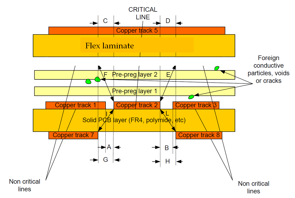 Figure 133: Example of double insulation by increasing distances in X,Y and by using two insulators in Z direction.
Insulation distance of combined requirements on rigid PCB
As-manufactured insulation distance shall be in conformance with the values specified in Table 137.
As-designed insulation distance should be in conformance with the values specified in Table 137.
As-designed insulation distance may be less than the values specified in the Table 137 in case the following conditions are met:
- a dedicated inspection is performed to verify that the as-manufactured insulation distance is in compliance with the values from the Table 137, and
- the insulation distance is recorded as a Review Item in the PCB definition dossier.
- 1 See the overview specified in clause 13.8.1 for a list of parameters that affect the insulation distance and that are included in the Table 137.
- 2 For legend to Table 137 see the overview in clause 13.1.
Table 137: Minimum insulation distances on rigid PCB as function of all combined requirements (part 1 of 4)
|
Insulation → |
Z laminate
|
Z prepreg
| |||||
|
standard
|
Double 13.9
|
standard
|
Double 13.9
| ||||
|
V (peak 13.8.2b)
|
Cu Th →
|
≤ 35 µm
|
70 µm
|
≤ 35 µm
|
70 µm
|
-
|
-
|
|
0<V≤10
|
As manufactured
|
70 µm
|
100 µm
|
70 µm
|
100 µm
| ||
|
As-designed
|
≥ 4mil 7.1.3f
|
≥ 5mil 7.1.3g
|
5mil screened 7.1.3g
|
-
|
-
| ||
|
10<V≤30
|
As-manufactured
|
70 µm
|
100 µm
|
70 µm
|
100 µm
| ||
|
As-designed
|
≥ 4mil 7.1.3f
|
≥ 5mil 7.1.3g
|
5mil screened 7.1.3g
|
-
|
-
| ||
|
30<V≤50
|
As-manufactured
|
100 µm
|
130 µm
|
100 µm
|
130 µm
| ||
|
As-designed
|
5mil screened 7.1.3g
|
See Table 72
|
-
|
-
| |||
|
50<V≤100
|
As-manufactured
|
100 µm
|
(1,5 µm/V AND 130 µm)
|
100 µm
|
(1,5 µm/V AND 130 µm)
| ||
|
As-designed
|
5mil screened 7.1.3g
|
See Table 72
|
-
|
-
| |||
|
100<V≤500
|
As-manufactured
|
1 µm/V
|
1,5 µm/V
|
1 µm/V
|
1,5 µm/V
| ||
|
As-designed
|
See Table 72
|
See Table 72
|
-
|
-
| |||
Table 137: Minimum insulation distances on rigid PCB as function of all combined requirements (continued 2 of 4)
|
Insulation → |
X,Y external without conformal coating
|
X,Y external with conformal coating
| |||||||||
|
standard
|
Double 13.9
|
standard
|
Double 13.9
| ||||||||
|
max tolerance in X,Y 7.4.2b →
|
50 µm
|
50 µm
|
70 µm
|
|
50 µm
|
50 µm
|
70 µm
|
50 µm
|
50 µm
|
70 µm
| |
|
V (peak 13.8.2b)
|
Cu Th →
|
fine pitch
|
normal pitch
|
normal pitch
|
|
fine pitch
|
normal pitch
|
normal pitch
|
fine pitch
|
normal pitch
|
normal pitch
|
|
0<V≤10
|
As-manufactured
|
not permitted
|
200 µm
|
280 µm
|
not permitted
|
120 µm
|
160 µm
|
240 µm
|
not permitted
|
320 µm
|
480 µm
|
|
As-designed
|
250 µm
|
350 µm
|
150 µm
|
200 µm
|
300 µm
|
370 µm
|
550 µm
| ||||
|
10<V≤30
|
As-manufactured
|
300 µm
|
380 µm
|
120 µm
|
160 µm
|
240 µm
|
320 µm
|
480 µm
| |||
|
As-designed
|
350 µm
|
450 µm
|
150 µm
|
200 µm
|
300 µm
|
370 µm
|
550 µm
| ||||
|
30<V≤50
|
As-manufactured
|
not permitted, except
|
not permitted
|
160 µm
|
240 µm
|
320 µm
|
480 µm
| ||||
|
As-designed
|
FOR 13.8.4d:
|
FOR 13.8.4d:
|
200 µm
|
300 µm
|
370 µm
|
550 µm
| |||||
|
50<V≤100
|
As-manufactured
|
not permitted, except
|
2 µm/V
|
240 µm
|
4 µm/V
|
480 µm
| |||||
|
As-designed
|
FOR 13.8.4d:
|
FOR 13.8.4d:
|
2,5 µm/V
|
300 µm
|
(4 µm/V + 50 µm)
|
550 µm
| |||||
|
100<V≤500
|
As-manufactured
|
not permitted, except
|
2 µm/V
|
2 µm/V
|
4 µm/V
|
4 µm/V
| |||||
|
As-designed
|
FOR 13.8.4d:
|
FOR 13.8.4d:
|
(2 µm/V +50µm)
|
(2 µm/V + 70µm)
|
(4 µm/V +50µm)
|
(4 µm/V +70µm)
| |||||
Table 137: Minimum insulation distances on rigid PCB as function of all combined requirements (continued 3 of 4)
|
Insulation →
|
X,Y internal conductor to conductor
| ||||||||||
|
standard
|
Double 13.9
| ||||||||||
|
max tolerance in X,Y 7.4.2b →
|
30 µm
|
30 µm
|
50 µm
|
50 µm
|
70 µm
|
30 µm
|
30 µm
|
50 µm
|
50 µm
|
70 µm
| |
|
V (peak 13.8.2b)
|
Cu Th →
|
fine pitch
|
normal pitch
|
17<Th≤60 µm
|
60<Th≤70 µm
|
70<Th≤95 µm
|
fine pitch
|
normal pitch
|
17<Th≤60 µm
|
60<Th≤70 µm
|
70<Th≤95 µm
|
|
0<V≤10
|
As-manufactured
|
FOR fine pitch 7.4.5a: 96 µm
|
104 µm
|
120 µm
|
160 µm
|
240 µm
|
not permitted
|
240 µm
|
240 µm
|
280 µm
|
360 µm
|
|
As-designed
|
FOR fine pitch 7.4.5a: 120 µmFOR 1mm pitch HDI 11.5.5a: 90 µm
|
130 µm
|
150 µm
|
200 µm
|
300 µm
|
270 µm
|
290 µm
|
330 µm
|
430 µm
| ||
|
10<V≤30
|
As-manufactured
|
FOR fine pitch 7.4.5a: 96 µm
|
104 µm
|
120 µm
|
160 µm
|
240 µm
|
240 µm
|
240 µm
|
280 µm
|
360 µm
| |
|
As-designed
|
FOR fine pitch 7.4.5a: 120 µm
|
130 µm
|
150 µm
|
200 µm
|
300 µm
|
270 µm
|
290 µm
|
330 µm
|
430 µm
| ||
|
30<V≤50
|
As-manufactured
|
not permitted
|
150 µm
|
150 µm
|
160 µm
|
240 µm
|
300 µm
|
300 µm
|
310 µm
|
390 µm
| |
|
As-designed
|
180 µm
|
188 µm
|
200 µm
|
300 µm
|
330 µm
|
350 µm
|
360 µm
|
460 µm
| |||
|
50<V≤100
|
As-manufactured
|
150 µm
|
150 µm
|
160 µm
|
240 µm
|
300 µm
|
300 µm
|
310 µm
|
390 µm
| ||
|
As-designed
|
180 µm
|
188 µm
|
200 µm
|
300 µm
|
330 µm
|
350 µm
|
360 µm
|
460 µm
| |||
|
100<V≤500
|
As-manufactured
|
1 µm/V
|
1 µm/V
|
1 µm/V
|
1 µm/V
|
2 µm/V
|
2 µm/V
|
2 µm/V
|
2 µm/V
| ||
|
As-designed
|
(1 µm/V +30µm)
|
(1 µm/V +50µm)
|
(1 µm/V +50µm)
|
(1 µm/V +70µm)
|
(2 µm/V +30µm)
|
(2 µm/V +50µm)
|
(2 µm/V +50µm)
|
(2 µm/V +70µm)
| |||
Table 137: Minimum insulation distances on rigid PCB as function of all combined requirements (continued 4 of 4)
|
Insulation → |
X,Y internal conductor to hole wall
|
X,Y internal hole wall to hole wall
| |||||
|
standard
|
Double 13.9
|
standard
|
Double 13.9
| ||||
|
max tolerance in X,Y 13.8.2iNOTE →
|
-
|
-
|
100 µm
|
300 µm
|
100 µm
|
300 µm
| |
|
V (peak 13.8.2b)
|
bond sequence →
|
-
|
-
|
single bond sequence
|
sequential bonding and rigid flex
|
single bond sequence
|
sequential bonding and rigid flex
|
|
0<V≤10
|
As-manufactured
|
X,Y internal + annular ring of 50 µm
|
350 µm
|
350 µm
|
700 µm
|
700 µm
| |
|
As-designed
|
450 µm
|
650 µm
|
800 µm
|
1000 µm
| |||
|
10<V≤30
|
As-manufactured
|
350 µm
|
350 µm
|
700 µm
|
700 µm
| ||
|
As-designed
|
450 µm
|
650 µm
|
800 µm
|
1000 µm
| |||
|
30<V≤50
|
As-manufactured
|
350 µm
|
350 µm
|
700 µm
|
700 µm
| ||
|
As-designed
|
450 µm
|
650 µm
|
800 µm
|
1000 µm
| |||
|
50<V≤100
|
As-manufactured
|
350 µm
|
350 µm
|
700 µm
|
700 µm
| ||
|
As-designed
|
450 µm
|
650 µm
|
800 µm
|
1000 µm
| |||
|
100<V≤500
|
As-manufactured
|
2 µm/V
|
2 µm/V
|
4 µm/V
|
4 µm/V
| ||
|
As-designed
|
(2 µm/V + 100 µm) AND 450 µm
|
(2 µm/V + 300 µm) AND 650 µm
|
(4 µm/V + 100 µm) AND 800 µm
|
(4 µm/V + 300 µm) AND 1000 µm
| |||
|
Note: The legend to this table is provided in Table 131.
| |||||||
Controlled impedance tracks
Definitions specific to controlled impedance
Microstrip is a track coupled to one copper plane. Stripline is a track between two copper planes. Stripline provides better shielding of the signals compared to microstrip, but it requires more plane layers.
Differential microstrip are two parallel tracks on the same layer and coupled to one copper plane. Differential striplines are two parallel tracks either edge coupled or broadside coupled and coupled to two copper planes.
For end to end configuration only a single driver and receiver is present at the extremes of a track. For multidrop configuration multiple drivers and receivers are possible along a track.
General rules
Controlled impedance tracks shall be recorded as a Review Item in the PCB definition dossier.
Controlled impedance tracks should be routed on a single layer.
Vias should not be used in controlled impedance tracks except for the connection of component pads.
The controlled impedance tracks should be designed with end-to-end configuration.
The controlled impedance tracks may be designed with multidrop configuration.
When using multidrop configuration the impedance calculation shall include the additional discrete loads.
Microstrip and stripline
Microstrip or stripline shall be used for single ended controlled impedance tracks.
Differential microstrip and differential stripline shall be used for differential controlled impedance tracks.
An example of edge coupled differential striplines is given in Figure 134. This figure shows the following characteristic dimensions used to calculate impedance:
- H: distance between planes as-manufactured
- H1: laminate thickness between tracks and plane.
- W: width of the top of the tracks
- W1: width of the foot of the tracks
- S: spacing between foot of tracks.
Differential tracks shall be routed in parallel without change of the distance between the tracks except the case specified in the requirement 13.11.3d.
Differential tracks may be routed non-parallel at the end of the track.
This is permitted to route to pads.
 Figure 134: Edge coupled differential striplines
Line impedance termination for end-to-end configuration
Series termination shall be used for end-to-end configuration.
The resistor for series termination shall be placed at the driver output.
AC parallel termination may be used in the end-to-end configuration at the input of the receiver.
Line impedance termination for multidrop configuration
Parallel termination shall be used in multidrop configuration.
DC or AC termination may be used in a multidrop configuration.
* AC termination can be preferred to save power.
In multidrop configuration with one driver and several receivers the driver shall be at one end of the line and the termination at the other end.
In multidrop configuration with several drivers and several receivers the line termination shall be at both ends of the line.
Digital PCB
Overview
Digital circuitries are those in which the information on a line can assume only two values “0” or “1”. They are, in general, more robust to noise with respect to the analog ones. They can be critical during the transition of the threshold region if the input signal is not monotonic.
The criticality of digital signals is indicated as non-critical, critical and highly critical. The criteria for criticality are not the same as for critical nets subject to double insulation as specified in the clause 13.9.2.
Zone management and routing
The layout of a PCB should be partitioned by using zone management where different logical blocks are physically separated from each other.
Different blocks to be separated in a board layout can be low speed (or static) links, analog links, power lines, high speed serial digital links, RF signals.
The low speed circuit should be separated from the high speed digital circuit.
High speed signals should not be routed through low speed zones.
This is done to prevent cross talk.
Ground planes shall be used in high speed digital applications.
Ground planes should be used in all digital applications.
High speed signals shall be routed over uninterrupted planes
Examples of uninterrupted planes are Vcc or GND.
The loop area of high speed signals should be minimised.
Loop area is minimised to reduce current noise. This can be achieved by routing the forwarded signal directly below or above a ground plane as return path. Further precautions can be found in the following references: chapter B.3.3 and B.3.4 of IPC-2251; chapter 6.4.6 of IPC-2221B.
Circuitry and components for high speed signals should be kept close together.
The length of routing in digital applications for high speed signals should be minimised, except when matched timing is used.
Reducing the length of signal paths is done, especially for high speed parallel links between components, to reduce crosstalk, voltage noise and adaptation of line impedance. This also achieves a more compact PCB design. The technology determines how to implement minimisation. For example, rise and fall time are more critical than frequency. Tracks length lower than “critical length” defined in Table 5-4 of IPC-2251 is an example of minimisation. When “critical length“ is exceeded, the tracks are considered as transmission lines. This is described in chapter 4.4.2.d of IPC-2251 and in IPC-2141A.
Criticality of digital signals
Non-critical signals
Signals that are not sensitive to the coupling between them shall be identified as “non-critical”.
Examples of non-critical signals are: data bus, address bus.
Non-critical signals specified in the requirement 13.12.3.1a may be routed together in bundles disregarding transients between them.
- 1 Transients are temporary anomalies in the electrical signal, such as overshoot, undershoot, ringing, lines reflection, crosstalk.
- 2 Transients are typically expired or reduced to an acceptable level before the sampling time.
Direct coupling between bundles of non-critical signals specified in the requirement 13.12.3.1a should be avoided.
Critical signals
Signals that require a monotonic waveform through the voltage threshold of the receivers shall be identified as “critical”.
Examples of critical signals are: clocks signals, write signals.
The routing of critical signals specified in the requirement 13.12.3.2a should maintain signal integrity at the receiver end.
Signal integrity tools can be used to simulate the behaviour of the PCB after routing.
The integrity of critical signals specified in the requirement 13.12.3.2a shall be verified by electrical testing of the PCB.
Highly critical signals
Signals that can affect the performance of the circuit as a result of noise, crosstalk, jitter, ringing or propagation delay, shall be identified as “highly critical”.
Examples of highly critical signals are: PLL signals, low voltage and high frequency LVDS signals.
Highly critical signals specified in the requirement 13.12.3.3a should be routed without adjacent signals or protected by shielding.
Separation of other highly critical signals is done to prevent crosstalk and noise pickup. Separation can be achieved by planes and rows of shielding vias.
The integrity of highly critical signals specified in the requirement 13.12.3.3a shall be verified by electrical testing of the PCB.
Analog PCB
Overview
PCB for analog circuitries are used to interconnect heterogeneous discrete components such as resistors, capacitors, diodes, transistors, amplifiers to implement an analog function. Analog circuitries are more susceptible to noise compared to digital circuitries. The PCB design can affect the overall performance. Analog signals include all values within a range. The criticality depends on the resolution or on the bandwidth of the signal.
The criticality of analog signals is indicated as non-critical, critical and highly critical. The criteria for criticality are not the same as for critical nets subject to double insulation as specified in the clause 13.9.2.
Criticality of analog signals
Non-critical signals
Signals that have low speed, low bandwidth or low resolution shall be identified as “non-critical”.
The signal-to-noise ratio, pickup and crosstalk noise (or any combination) are non-critical for such signals. These signals do not affect the performance or the functionality of the equipment.
Critical signals
Signals for which signal-to-noise ratio, pickup or crosstalk noise can affect performance of a circuit shall be identified as “critical”.
Examples of critical signals are: feedback signals of control loop of series and switching regulators.
Highly critical signals
Signals with high speed or high bandwidth or low amplitude or high resolution shall be identified as “highly critical”.
The performance degradation of such signals can affect the functionality of the equipment.
The parasitic inductance of a track and the parasitic capacitance of a pad can affect high speed analog circuit performance.
The length of a track connecting an inverted input of a high speed amplifier with a passive component should be minimised.
This reduces the noise coupling to high impedance input of the amplifier. The objective is to guarantee the noise performance of the amplifier.
Highly critical circuitry specified in the requirement 13.13.2.3a shall have priority in the design, placement and routing.
Routing and shielding
Ground planes shall be used for critical and highly critical analog circuitries specified in the requirements 13.13.2.2a and13.13.2.3a.
Ground planes should be used for non-critical analog circuitries specified in the requirement 13.13.2.1a.
* Ground planes shield signals from pickup noise.
The track length of high impedance signals should be minimized.
This is done to reduce crosstalk and pickup noise.
High impedance signals should be shielded or have guard rings implemented.
“Set on test” components should be placed near to the adjusted component.
Test point and jumpers for analog circuitry should be placed near to the circuit that requires adjustment.
Examples of circuit that can require adjustment are: series regulator, voltage reference, DC/DC converters.
Mixed analog-digital PCB
Analog and digital circuitry on the same PCB shall be separated from each other by zone management and shielding.
Planes of analog and digital circuitries should be separated.
Superimposed analog and digital planes can result in AC coupling and digital noise on the analog signal.
Planes of analog and digital circuitries may be combined in case separation of the planes has an adverse effect on performance or functionality or EMC.
In case planes of analog and digital circuitries are combined, power supply decoupling shall be implemented.
Digital signals should not be routed through analog zones.
The accurate routing of the analog and digital signals is important for DAC, ADC and MUX applications.
Design for assembly
Overview
The requirements in this clause apply to the design of the PCB for PCB assembly by internal or external assembly house. The surface pattern of the PCB depends on the PCB geometry, the assembly method and the location of mechanical and external elements.
General
When PCB design and PCB assembly are performed in different companies, the supplier shall confirm with the assembly house which assembly processes are used.
Pad geometry and outer layers shall be reviewed by the assembly house for potential assembly problems in compliance with requirements from clause 5 to clause 15 of ECSS-Q-ST-70-08 and in compliance with requirements from clause 5 to clause 16 of ECSS-Q-ST-70-38.
Pad geometry and outer layers shall be approved by the assembly house in compliance with requirements from clause 5 to clause 15 of ECSS-Q-ST-70-08 and in compliance with requirements from clause 5 to clause 16 of ECSS-Q-ST-70-38.
Assemblies using SnPb solder alloys shall not be used on gold plated pads in conformance with the requirements 6.8.2a of the ECSS-Q-ST-70-08.
Today Electroless Nickel–Palladium Immersion gold surface finish is under evaluation.
Placement requirements
Conductive patterns
The distance of the surface pattern to the adjacent surroundings shall be in conformance with values specified in Table 141.
An illustration is given in Figure 141.
Table 141: Minimum distance as-manufactured of the surface pattern to the adjacent surroundings
|
Dimension
|
Description
|
Permitted
|
Recommended
|
|
A 1
|
Dimension between track and PCB edge
|
0,7 mm
|
|
|
A 2
|
Dimension between track and mechanical part
|
1,0 mm
|
2,0 mm
|
|
A 3
|
Dimension between track and non-plated through hole
|
0,4 mm
|
|
|
A 4
|
Dimension between via pad and hole for mechanical function
|
1,0 mm
|
|
|
A 5
|
Dimension between track and screw
|
0,5 mm
|
|
|
A 6
|
Dimension between conductive surface pattern and PCB edge
|
0,25 mm
|
|
|
A 7
|
Dimension between edge of screw hole and PCB edge
|
1,0 mm
|
1,5 mm
|
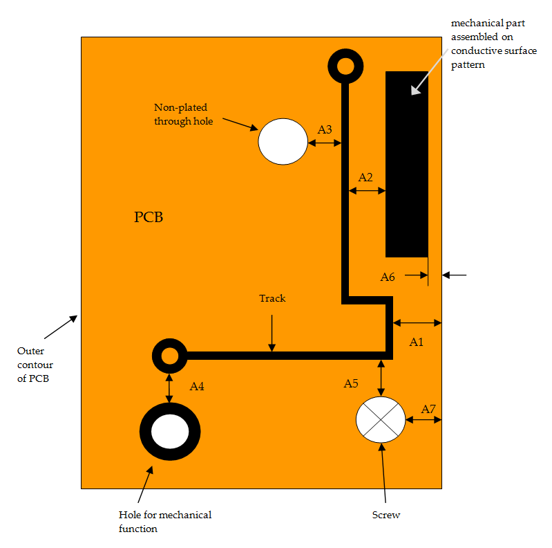 Figure 141: Illustration of surface pattern to adjacent surroundings
Components
The conductive parts of components shall not be in contact with each other or with any metal in their adjacent surroundings.
For example screws, rack, and structure.
The distance of components to adjacent surroundings shall be in conformance with values specified in Table 142.
An illustration is given in Figure 142.
The width of the zone without components along the PCB edges should be ≥ 5 mm.
This is done to provide a clearance for the conveyor in the assembly equipment.
In case the lay-out of the PCB requires the restricted zone to be less than 5 mm from the edge of the PCB, the PCB assembly house shall be consulted.
Table 142: Minimum distance as-manufactured of components to adjacent surroundings
|
Minimum dimension
|
Description
|
Permitted data
|
Recommended data
|
|
B 1
|
Distance between component body to component body, one of which is non-conductive
|
> 0 mm, in case that precautions are taken to prevent damage during vibration.
|
0,6 mm
|
|
B 2
|
Distance between component lead and cover (of electronic box)
|
1,0 mm
|
1,0 mm
|
|
B 3
|
Component lead to component lead (B3-a)
|
0,5 mm
|
1,0 mm
|
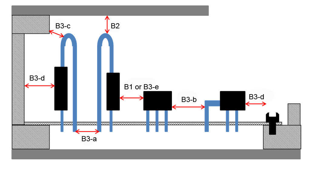 Figure 142: Illustration of component placing on PCB w.r.t. adjacent surrounding
Component pads
Design for assembly on component pads shall be in conformance with requirements from the clause 8 of ECSS-Q-ST-70-08 and clause 11 of ECSS-Q-ST-70-38.
The distance of component pads to adjacent surroundings shall be in conformance with values specified in Table 143.
An illustration is given in Figure 143
The location of the devices shall be such that each solder connection can be visually inspected.
High components should not be placed close together.
This is done to enable repair by manual soldering.
Around an AAD a clearance should be implemented for repair.
Requirements for PCB repair are specified in ECSS-Q-ST-70-28.
For PCBs submitted to conveyor wave soldering, components and tracks should be oriented in the solder direction.
Designed test points shall be separated from the component solder pads.
Test points may be incorporated in the solder pad by extending the pad dimensions so that test probing takes place outside the critical solder joint area in conformance with requirements 12.3.a.22 of the ECSS-Q-ST-70-08 and 13.3.a.21 of the ECSS-Q-ST-70-38.
The extended pad shall be included in the assembly qualification as the extra size affects the volume of solder in the joint.
Thermal relief shall be designed between component PTH and copper planes.
Table 143: Minimum distance as-manufactured to component pads
|
Minimum dimension
|
Description
|
Permitted data
|
|
A, B, C, G, J
|
- Dimension between pads of PTH on solder side
|
0,3 mm
|
|
D, E, H, I
|
- Dimension between pads of PTH on component side
|
0,5 mm
|
|
F
|
Dimension between component body to pad
|
0,5 mm
|
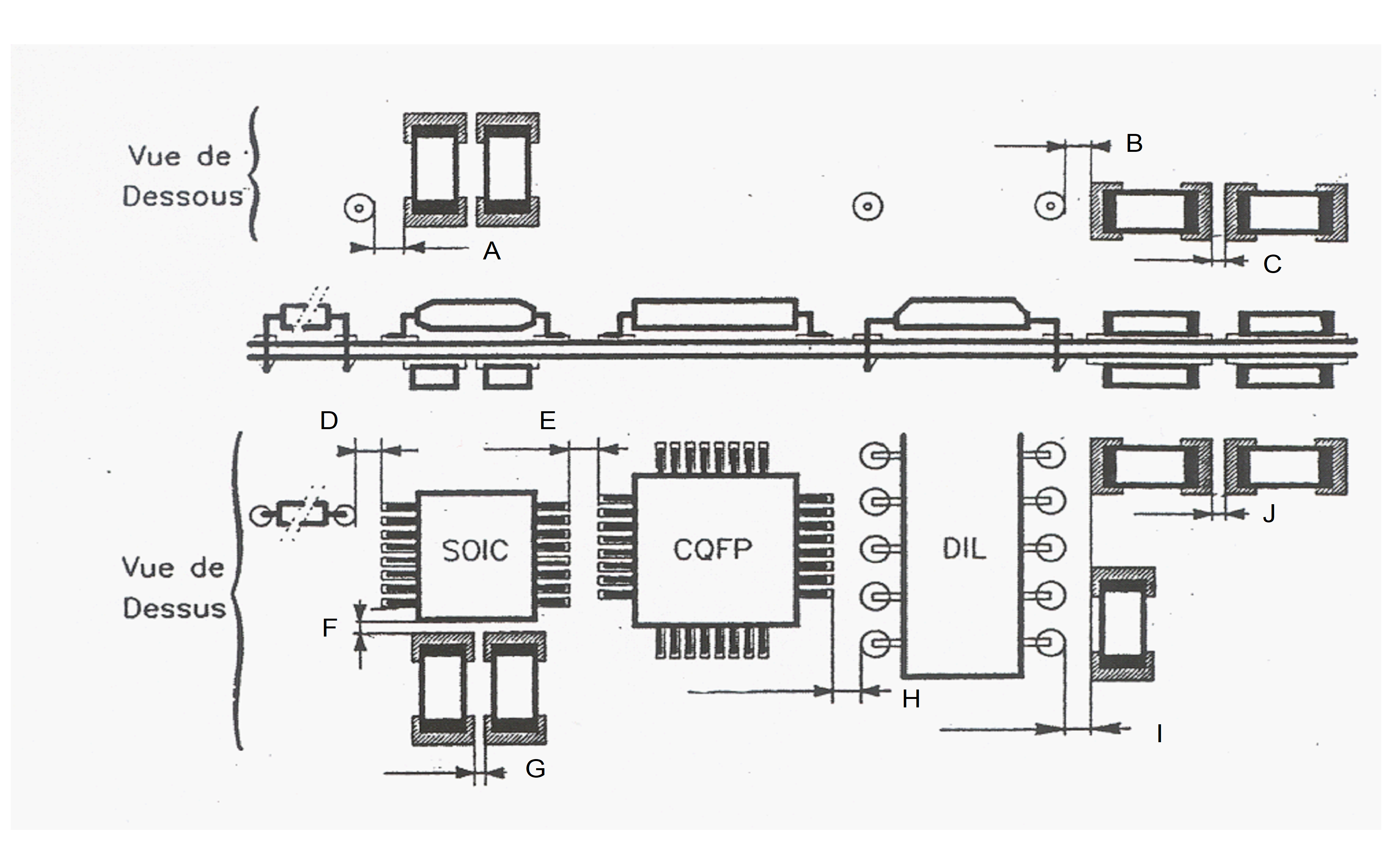 Figure 143: Illustration of pad placing on PCB with respect to adjacent surroundings
Fan out of SMT pads
The track length between SMT pad and via shall be in conformance with values specified in Table 144
- 1 In Figure 144: LT is the track length between SMT and via.
- 2 The through going via can absorb all tin-lead away from the pad during assembly.
For other track dimensions, the supplier shall extrapolate or interpolate from the values specified in requirement 14.3.4a.
Larger distances are preferred, even though tracks are avoided on external layers.
The fan out should be symmetric.
This is done to avoid unwanted movement of components during reflow soldering. An example of a symmetric fan out is given in Figure 144.
The SMT pad of an AAD may be asymmetric.
Examples of asymmetric SMT pad are key hole, solder verification snip. The purpose of this is to verify quality of the solder joint.
The four quadrants of the total footprint of the AAD shall be designed point symmetric such that each quadrant has the asymmetry in four directions.
This is done to prevent the component drifting away from the footprint during assembly. An example of a point symmetric AAD footprint is given in Figure 145.
The width of the track connecting to an SMT pad of a chip device shall be ≤ 1/3 of the width of the pad.
- 1 An illustration of fan out from SMT pad is given in Figure 144.
- 2 In Figure 144: WT is the width of the track connecting to an SMT pad of a chip device, and WP is width of the pad
- 3 This is done for thermal relief to prevent the track acting as a heat sink and removing heat from the pad during assembly.
- 4 This requirement is defined for chip devices not for flat packs.
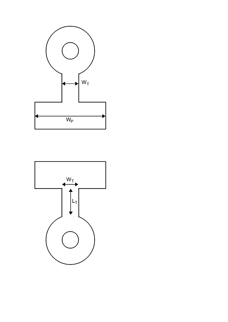 Figure 144: Fan out from SMT pad to via
Table 144: Minimum track length to component pads
|
WT [mm]
|
LT [mm]
|
|
0,2
|
≥ 0,25
|
|
0,3
|
≥ 0,7
|
 Figure 145: Example of point symmetric AAD footprint
### Fan out of PTH
The track width connecting to soldering pad of PTH shall be maximum half of the diameter of the pad.
- 1 An illustration of track connecting to soldering pad is shown in Figure 146
- 2 In Figure 146: Ic is the track width connecting to soldering pad of PTH with diameter D.
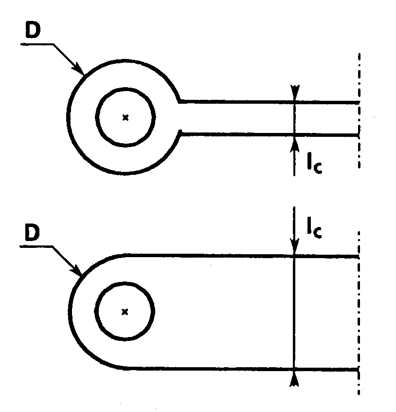 Figure 146: Track width (Ic) ratio to PTH pad (D) diameter.
The track length between soldering pad of PTH and via shall be at least half the diameter of the largest pad
- 1 An illustration of track between soldering pad and via is shown in Figure 147.
- 2 In Figure 147: Lc is the track length between soldering pad of PTH with diameter D1 and via pad with diameter D3.
 Figure 147: Track length (Lc) between soldering pad of PTH (D1) and via pad (D3)
Specific requirements for fused tin-lead finish
Adhesive bonding should not be performed on fused tin-lead.
Bonded devices shall have clearance for spot bonding.
Dimensional requirements for SMT foot print
Overview
The design rules of this clause apply for new pad designs. Successful assembly verification justifies the use of existing pad designs provided that minimum insulation distance is achieved, as specified in requirement 14.5.2c. This requirement defines permission for continued use of pad designs that have been successfully verified prior to the first issue date of this standard.
The use of blind via in component pad can act as a heat sink.
This clause specifies as-manufactured pad dimensions for various component footprints. The as-designed pad dimensions depend on following:
the etching tolerance for the surface copper thickness,
etching undercut
tolerance of component dimensions
minimum width of solder fillet
misalignment of component on footprint
Table 145 Legend for dimensions of components and footprint
|
Minimum dimension
|
Description
|
|
i
|
insulation distance
|
|
M1
|
Solder fillet
|
|
M2
| |
|
M3
| |
|
X
|
Width of pad
|
|
AA
|
Distance between pads
|
|
BB
|
Total length of pad footprint
|
|
Y
|
Length of pad
|
|
L, E
|
Length of component
|
|
T
|
Length of termination
|
|
W, C
|
Width of termination
|
|
P
|
Pitch of AAD
|
|
D
|
Diameter of pad for AAD
|
General
Insulation distance shall be in conformance with requirements of clauses 13.8, 13.9 and 13.10.
The largest distance shall be used in case the distance between pads specified as AA in Table 146, Table 147, Table 148, Table 149 and Table 1410 is smaller than the insulation distance specified in the requirement 14.5.2a.
- 1 Insulation distance is indicated with the letter “i” in Figure 148, Figure 149, Figure 1410, Figure 1411, Figure 1412 and Figure 1413.
- 2 The minimum insulation distance applies to all pad designs, including existing pad designs, new pad designs and pad designs not specified in this standard.
Existing pad designs may deviate from the requirements of clauses 14.5.3 to 14.5.7, in case the following conditions are met:
the existing pad designs have been already verified in accordance with clause 14 of ECSS-Q-ST-70-38 prior to the first issue date of ECSS-Q-ST-70-12, and
insulation distance is in conformance with requirement 14.5.2a.
For background on requirement 14.5.2c see clause 14.5.1.
Pad designs of components that are not specified in requirements from clauses 14.5.3 to 14.5.8 shall be designed in compliance with the manufacturer’s datasheet and requirements from clause 14.5.2a.
Bipolar components
The pad design for bipolar components shall be in conformance with the as-manufactured values specified in the Table 146, except for the case specified in 14.5.2c
- 1 Examples of bipolar components are: cylindrical, rectangular and square end-capped devices
- 2 An illustration is given in Figure 148.
 Figure 148:Illustration of bipolar component pads
Table 146 As-manufactured pad sizes for bipolar components
|
Minimum dimension
|
Permitted data
|
|
M1
|
0,2 mm
|
|
M2
|
0,1 mm
|
|
M3
|
> 0 mm
|
|
X
|
Wmax+ 2*M3
|
|
AA
|
Lmin-2*(Tmax + M2)
|
|
BB
|
Lmax+2*M1
|
|
Y
|

|
SOIC components
The pad design for components of type SOIC with gullwing-leads shall be in conformance with the as-manufactured values specified in Table 147, except for the case specified in 14.5.2c.
An illustration is given in Figure 149.
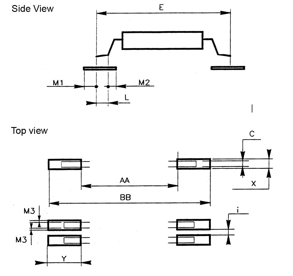 Figure 149: Illustration of SOIC component pads
Table 147: As-manufactured pad sizes for SOIC components
|
Minimum dimension
|
Permitted data
|
|
M1
|
0,2 mm
|
|
M2
|
0,2 mm
|
|
M3
|
> 0 mm
|
|
X
|
Cmax+ 2*M3
|
|
AA
|
Emin-2*(Lmax + M2)
|
|
BB
|
Emax+2*M1
|
|
Y
|

|
J-leaded components
The pad design for components with J-leads shall be in conformance with the as-manufactured values specified in Table 148, except for the case specified in 14.5.2c.
An illustration is given in Figure 1410.
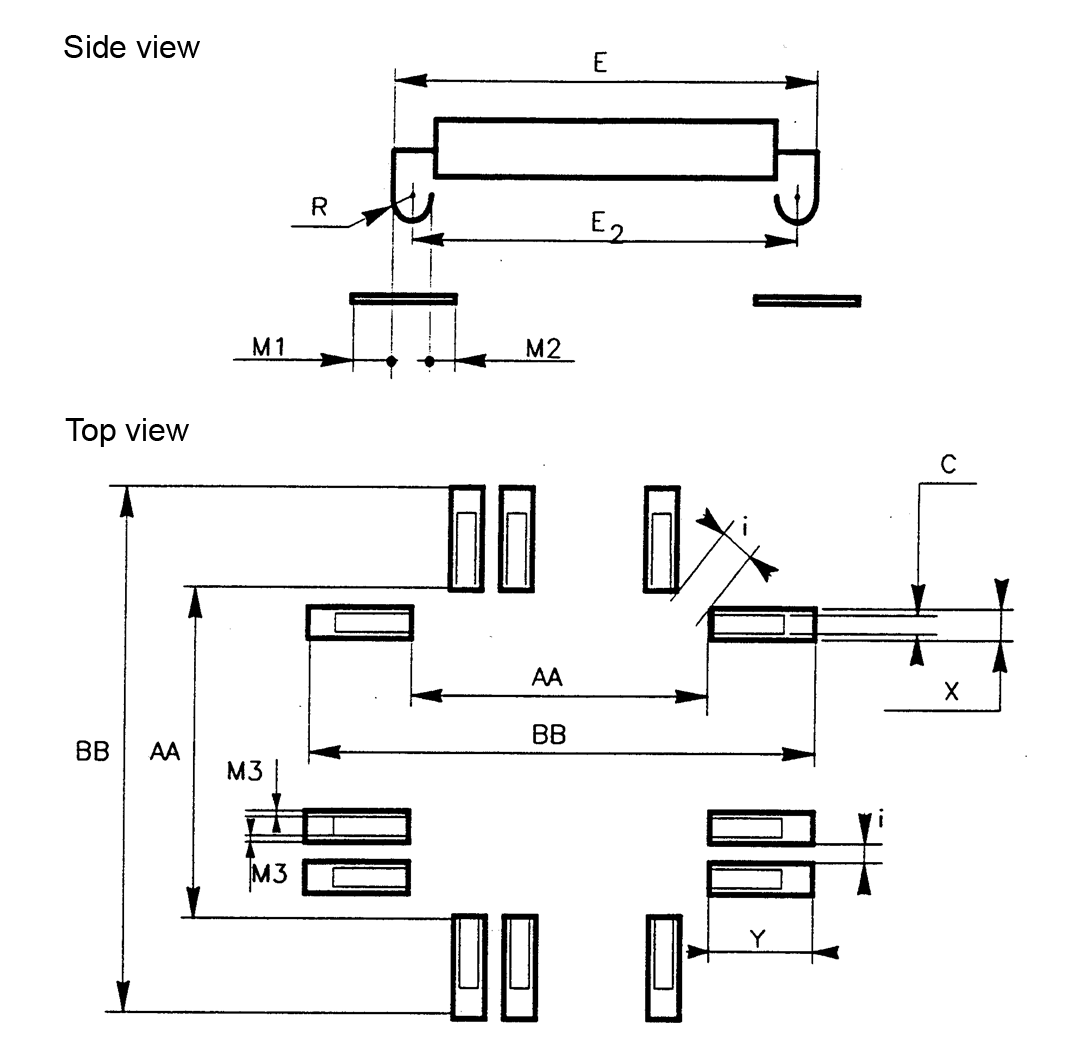 Figure 1410: Illustration of J-leaded component pads
Table 148: As-manufactured pad sizes for J-leaded components
|
Minimum dimension
|
Permitted data
|
|
M1
|
0,2 mm
|
|
M2
|
0,2 mm
|
|
M3
|
> 0 mm
|
|
X
|
Cmax+ 2*M3
|
|
AA
|
E2 min-2*(Rmax + M2)
|
|
BB
|
Emax+2*M1
|
|
Y
|

|
LCC components
The pad design for components of type LCC shall be in conformance with the as-manufactured values specified in the Table 149, except for the case specified in 14.5.2c.
- 1 An illustration is given in Figure 1411.
- 2 LCC means leadless chip carrier.
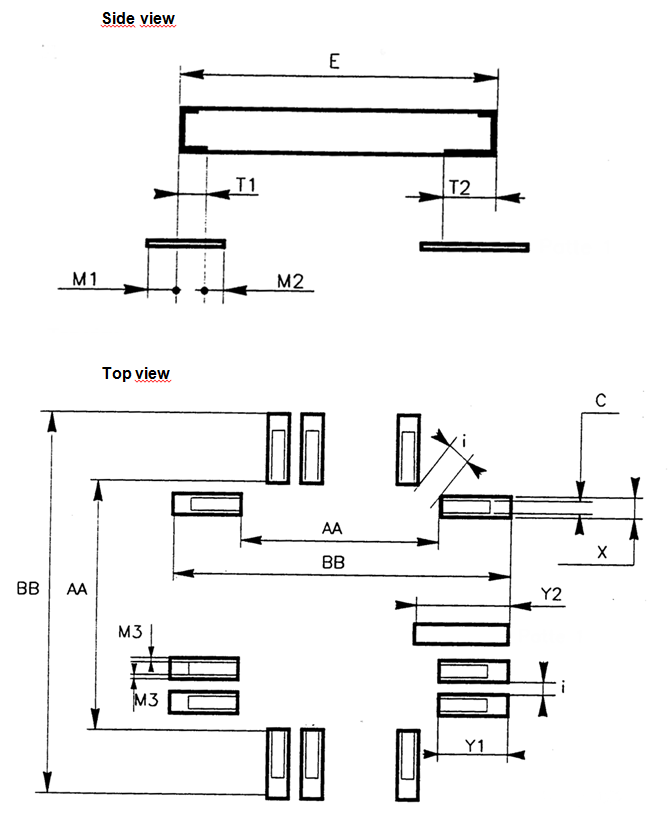 Figure 1411: Illustration of LCC component pads
Table 149: As-manufactured pad sizes for LCC components
|
Minimum dimension
|
Permitted data
|
|
M1
|
0,2 mm
|
|
M2
|
0,2 mm
|
|
M3
|
> 0 mm
|
|
X
|
Cmax+ 2*M3
|
|
AA
|
Emin-2*(T1+ M2)
|
|
BB
|
Emax+2*M1
|
|
Y1
|

|
|
Y2
|
Y1+(T2- T1)
|
Flat pack components
The pad design for components of type FP and QFP shall be in conformance with the as-manufactured values specified in the Table 1410, except for the case specified in 14.5.2c.
- 1 An illustration is given in Figure 1412.
- 2 FP means flat pack. QFP means quad flat pack.
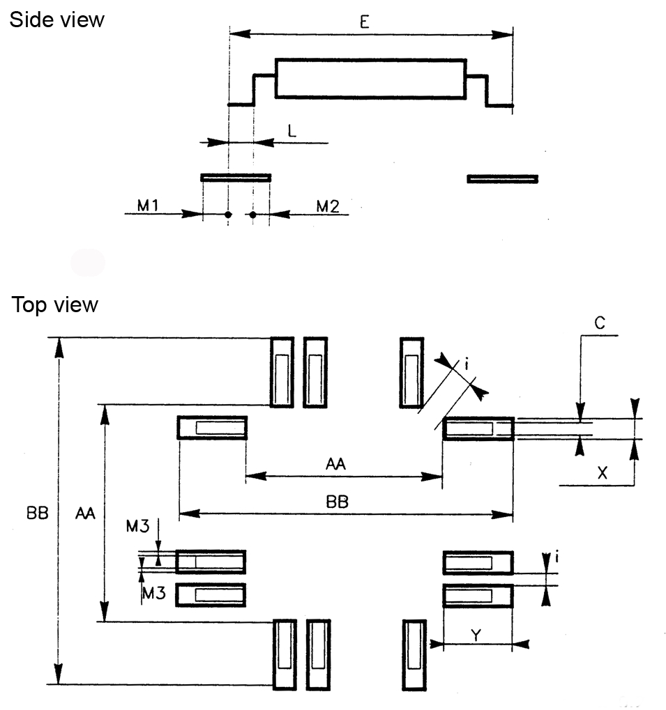 Figure 1412: Illustration of FP and QFP component pads
Table 1410: As-manufactured pad sizes for FP and QFP components
|
Minimum dimension
|
Permitted data
|
|
M1
|
0,2 mm
|
|
M2
|
0,2 mm
|
|
M3
|
> 0 mm
|
|
X
|
Cmax+ 2*M3
|
|
AA
|
Emin-2*(Lmax + M2)
|
|
BB
|
Emax+2*M1
|
|
Y
|

|
AAD components
The pad design for components of type AAD should be in conformance with the as-designed values specified in Table 1411.
An illustration of circular pad design for AAD footprint is given in Figure 1413. An illustration of teardrop pad design of AAD footprint is given in Figure 145.
The pad design for components of type AAD should be circular or with teardrop.
The pad design for components of type AAD should be with via-in-pad technology.
 Figure 1413: Illustration of AAD component pads
Table 1411: As-designed pad diameter for AAD components
|
Component pitch (P)
|
Minimum pad diameter (D)
|
|
1,27 mm
|
0,7 mm
|
|
1,0 mm
|
0,6 mm
|
Design of test coupon
Design rules for test coupon
The supplier shall be accountable for the design of the test coupon in conformance with requirements from the Clause 15.
The design of the test coupon shall be indicated as a Review Item.
It is common practice that the PCB manufacturer designs the coupon on behalf of the supplier. However, these requirements ensure that the supplier verifies the design of the coupon and has the end responsibility.
Test coupon design
The test coupon design should be representative of the PCB.
In case the PCB design is complex and the coupon cannot be designed with full representativity, the inspection on the coupon should be supplemented by a FAI.
The different density of a coupon compared to the rest of the PCB can limit the representativity. A higher copper density of the footprint of an AAD compared to a typical coupon design can cause a lower plating thickness. The higher via density of the footprint of an AAD can cause problems with resin flow and filling, which can remain undetected in a coupon of different density. High pressure areas local within the PCB can cause lower dielectric spacing compared to the coupon.
Test coupon location in the manufacturing panel should be representative of the worst case.
Worst-case location for registration is typically on the corners of the panel. However, worst-case for plating is typically in the centre of the panel. In this case, it is important the PCB manufacturer compares the plating thickness in the coupon with the rest of the panel. This is typically verified during qualification.
The following specific features shall be represented on the coupon in the same configuration as on the PCB:
- PCB build-up,
- Copper planes,
- Non-functional pads,
- Internal heat sinks,
- Hole types as follows:
- PTH for components
- Through-hole vias
- Blind vias
- Buried vias
- Microvias in the same configuration as on the PCB
- The minimum hole size of each type.
- The pad stack with the minimum pad diameter
- Either the maximum component hole size or the most frequently used component hole size.
- The minimum track width and spacing on each layer.
- All used surface finishes and overlap zones in conformance with requirement 7.8.1d.1.
- All plating, drilling and lamination sequences.
- Backdrilling of vias.
- Embedded film resistors of highest and lowest resistance
- Flex layers including cut-out and cover layer placement
- 1 Minimum hole size is included into requirement 15.2d.6 to verify plating in maximum aspect ratio holes.
- 2 The pad stack with minimum pad diameter is included into requirement 15.2d.7 to verify worst-case annular ring as-manufactured and registration.
- 3 In the requirement 15.2d.8 the supplier can decide which hole sizes to be incorporated on the coupon.
- 4 Minimum track width and spacing is included into requirement 15.2d.9 to be verified as function of copper thickness on a dedicated pattern.
In case teardrop reinforcement is used on the PCB, the following conditions shall be designed on the coupon: - the teardrop reinforcement is not included on the coupon, and
- the minimum pad diameter is included on the coupon.
This is done to ensure the annular ring requirement specified in the 11.5.2a.3 (i.e. 25 µm) is achieved without teardrop reinforcement.
The coupons shall be capable of completing the following tests:
- Thermal tests:
- Solderability,
- Rework Simulation,
- Thermal Stress.
- Mechanical tests:
- Peel strength,
- Pull-off test,
- Flex bend cycles,
- Tape bond test.
- Electrical tests:
- Insulation resistance,
- Interconnection resistance and continuity test,
- Inter-layer dielectric withstanding voltage,
- Controlled impedance,
- Embedded film resistance.
- Dimensional inspection:
- Annular ring,
- Track width and spacing.
- Inspection of general aspect in microsections. A dedicated coupon pattern shall be implemented to verify controlled impedances, when used on the PCB.
This dedicated coupon can be designed by the PCB manufacturer.
With multiple small PCBs on a panel, a spare PCB may be used instead of a coupon.
Each coupon shall have a serial number that ensures traceability to the panel.
ANNEX(normative)PCB definition dossier - DRD
DRD identification
Requirement identification and source document
This DRD is called from ECSS-Q-ST-70-12 requirement 5.2a.
Purpose and objective
The PCB definition dossier specifies the design and contains all information required for the tooling. The PCB definition dossier is part of the PCB manufacturing dossier under approval in the MRR.
Expected response
Scope and content
General
The PCB definition dossier shall include the following data:
- Description, as specified in A.2.1<2>,
- Mechanical layout, as specified in A.2.1<3>,
- Artwork data , as specified in A.2.1<4>,
- Drawing, as specified in A.2.1<5>,
- Specific electrical test, as specified in A.2.1<6>,
- Review Items , as specified in A.2.1<7>,
- Check list, as specified in A.2.1<8>, Description
The PCB definition dossier shall include a description containing at least the following data:
- Base material,
- Finishes,
- Number of layers,
- Size,
- Thickness and tolerance,
- Part number of PCB design: specified by supplier,
- Revision number of PCB design,
- Heat sink including:
- Heat sink thickness,
- Tolerances permitted,
- Material used,
- Type of protective surface coating.
Synonyms of revision number in requirement 7 are issue number and version number.
Mechanical layout
The PCB definition dossier shall include the mechanical layout containing at least the following data:
- One or more mechanical drawings including a dimensioning system,
- Location and form for the PCB manufacturer to place date code and serialization.
- 1 It is recommended in the requirement 1 to use a reference hole as datum point. The reference hole is recommended to be drilled in the first drill cycle.
- 2 The form of numbering as specified in requirement 2 can be in ink or conductive pattern.
- 3 An example of mechanical layout is shown in Figure A-1.
Artwork data
The PCB definition dossier shall include the artwork data containing at least the following information:
- Artwork data of each conductive PCB layer,
- Artwork data for non-conductive layers,
- Drilling and milling files.
- 1 Examples of conductive layers for the requirement 1 are circuitry and selective finishes.
- 2 Examples of non-conductive layers for the requirement 2 are solder mask and silk screen
- 3 It is preferred in the requirement 3 to distinguish by different tool codes the plated and non-plated holes in the drill file even if they have identical diameter.
- 4 For example, ODB++ is a format that describes all artwork of all layers in one file.
Drawing
The PCB definition dossier shall include the drawings containing at least the following:
- Drilling drawing,
- Drilling tables, including:
- Symbol,
- Diameter of as-manufactured holes,
- Tolerance,
- Plated or not plated,
- Quantity.
- Build-up data, including:
- Numbered conductive layers from top to bottom,
- Total copper thickness, basic + plated, for each layers with tolerances,
- Presence of planes: ground and supply, mesh plane or full copper,
- Presence of layers with controlled impedance,
- Thickness tolerance of laminate and prepreg, including minimum as-manufactured insulation distances,
- Total PCB thickness and tolerance,
- Specification if thickness is measured over bare laminate or over conductive pattern,
- Specific requirements for build-up.
- 1 Examples of specific requirements for build-up are:
- style of prepreg and laminate,
- use of separate copper foil or copper cladding on laminate for external layers,
- use of single or double sided laminate,
- use of two individually cured insulators to achieve double insulation.
- 2 Examples of Drilling drawing, Drilling table and Build-up data are given in Figure A-2, Figure A-3, Figure A-4.
Electrical test
The PCB definition dossier shall include the electrical test description containing at least the following data:
- Netlist,
- Definition of any electrical tests that are specific to the PCB design and in addition to the standard set of electrical tests,
- Identification of conductive lines that are designed to be of higher DC resistance that are at risk not to pass standard continuity testing,
- The definition of controlled impedance tracks including:
- Reference planes,
- Type of coupling,
- Track dimensions, including height, width, cross section,
- Spacing dimensions in X,Y and in Z direction,
- Impedance value, tolerance and method of measurement.
- Identification of any deliberate errors.
- 1 Example for requirement 4(b): broadside coupled, edge coupled.
- 2 In the requirement 4(e) the standard method for measuring impedance and tolerance is TDR in case the method is not specified
- 3 Example for the requirement 5 are differences between artwork and net list such as star points.
Review Items
The PCB definition dossier shall include all Review Items.
The following design features are required to be recorded as Review Items by the present standard:
Asymmetric build-up as specified in 7.1.1b,Molybdenum or CIC layers as specified in 7.1.1cAsymmetric copper cladding as specified in 7.1.2b,Total copper thickness >700 µm as specified in 7.1.2g, Single sheet of glass reinforcement in laminate as specified in 7.1.3c,4 mil laminate as specified in 7.1.3f,5 mil laminate at >30V as specified in 7.1.3g,Total PCB thickness as specified 7.3.2c and 7.3.3c,Reduced as-designed track width and spacing as specified in 7.4.3c and 7.4.4c,Fine pitch tracks as specified in 7.4.3g, and 7.4.5b,Removal of non-functional pads as specified in 7.5.1c,Reduced as-designed pad dimensions on solder side and component side as specified 7.5.2e and 7.5.2g,Pad diameter on rigid laminate <0,3mm larger than drilled hole as specified in 7.5.2i,Non-circular pads as specified in 7.5.3bAsymmetric copper planes as specified in 7.6e,Mixed surface finish as specified in 7.8.1e,70 µm copper cladding in flex laminate as specified in 8.3.3c,Full copper planes in flex laminate as specified in 8.3.4b,70 µm copper foil in combination with no-flow prepreg as specified in 9.3d,More than 2 flex laminates as specified in 9.3f, Pad diameter on flex laminates <0,6 mm larger than diameter of drilled hole as specified in 9.6b,Heat sinks and their mechanical stability as specified in 10.2a, 10.3.3a and 10.4.4a.Conductive surface pattern below external heat sink as specified in 10.3.2g,HDI as specified in 11.2c,Basic copper layer thickness <17 µm as specified in 11.4.1e,Diameter of external pad of microvia <0,15 mm larger than the ablated hole as specified in 11.4.3b,Reduced annular ring with teardrop reinforcement as specified in 11.5.2a,Differential pair routed in 1 mm pitch AAD footprint as specified in 11.5.5a,Aspect ratio of vias >7 for 1 mm pitch AAD footprint as specified in 11.5.6a,Embedded film resistors as specified in the requirements 12.3a and 12.3i,Thickness of RF PCB >3mm as specified in 12.4b,Number of layers in RF PCB >8 as specified in 12.4d,Reduced insulation distance for RF elements as specified in 12.5.1b,Z-controlled backdrilling as specified in 12.8a,Profiled top layers as specified in 12.8b,Profiled aluminium backing as specified in 12.8c,Reduced as–designed insulation distance as specified in 13.10c,Controlled impedance tracks as specified in 13.11.2,Design of test coupon as specified in 15.1b.The PCB definition dossier shall include all specific inspections required for the Review Items.
Check list
The PCB definition dossier shall include a check list containing at least the following data:
- all file names included in the archive,
- last modified data of each file,
- size of the file,
- CRC.
- The purpose of the check list is to define the content of the archive file to prevent transmission of wrong data. In Figure A-5 an example of a check list is shown. The check list indicates the content of the archive file by the four items mentioned in A.2.1<8>.
Special remarks
The format of the data of the PCB definition dossier shall be agreed between supplier and PCB manufacturer.
One single file should be used for transferring the data between supplier and PCB manufacturer.
The transmitted file should be an archive with lossless compression.
Examples of file extensions of archives with lossless compression are: .zip, .rar,.7z, .tar.
The supplier shall ensure the file format enables verification of file integrity to prevent corruption.
For example verification by CRC.
Example figures
 Figure: Example of PCB mechanical layout
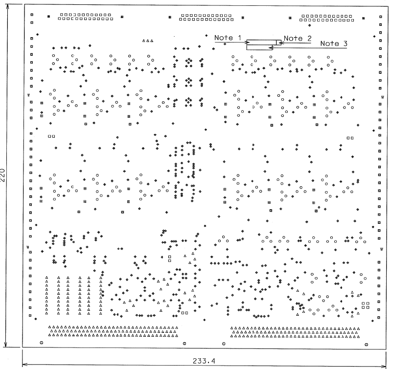 Figure: Example of a drilling drawing
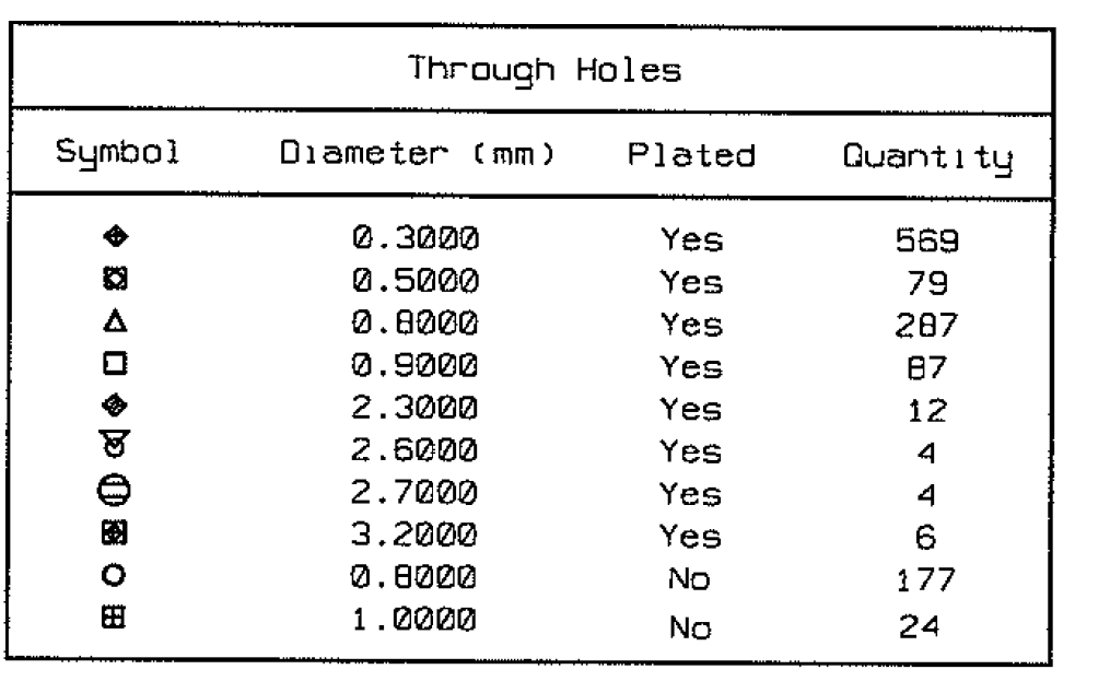 Figure: Example of a table indicating as-designed plated hole diameters
|
|
Stack
|
Insulation thickness (as-manufactured board)
|
Copper plane
|
Base copper thick-ness
|
|
|
Drilling
|
|
sequence
|
|
|
|
Total copper thickness (as-manufactured board)
|
|
Number of layers
| |
|
|
|
(m)
|
|
(m)
|
|
|
1
|
|
2
|
|
3
|
|
As-designed (m)
|
Tolerances
|
|
|
|
1
|
|
|
|
17
|
|
|
|
|
|
|
|
|
77,5
|
±30%
|
1
| |
|
|
|
100µm min
|
|
|
|
|
|
|
|
|
|
|
|
|
|
|
|
2
|
|
|
|
35
|
|
|
|
|
|
|
|
|
35
|
±20%
|
2
| |
|
|
|
100µm min
|
|
|
|
|
|
|
|
|
|
|
|
|
|
|
|
3
|
|
|
|
35
|
|
|
|
|
|
|
|
|
35
|
±20%
|
3
| |
|
|
|
100µm min
|
|
|
|
|
|
|
|
|
|
|
|
|
|
|
|
4
|
|
|
|
35
|
|
|
|
|
|
|
|
|
35
|
±20%
|
4
| |
|
|
|
100µm min
|
|
|
|
|
|
|
|
|
|
|
|
|
|
|
|
5
|
|
|
|
35
|
|
|
|
|
|
|
|
|
35
|
±20%
|
5
| |
|
|
|
100µm min
|
|
|
|
|
|
|
|
|
|
|
|
|
|
|
|
6
|
|
|
|
35
|
|
|
|
|
|
|
|
|
35
|
±20%
|
6
| |
|
|
|
100µm min
|
|
|
|
|
|
|
|
|
|
|
|
|
|
|
|
7
|
|
|
Yes
|
35
|
|
|
|
|
|
|
|
|
35
|
±20%
|
7
| |
|
|
|
100µm min
|
|
|
|
|
|
|
|
|
|
|
|
|
|
|
|
8
|
|
|
Yes
|
35
|
|
|
|
|
|
|
|
|
60
|
±20%
|
8
| |
|
|
|
100µm min
|
|
|
|
|
|
|
|
|
|
|
|
|
|
|
|
9
|
|
|
Yes
|
35
|
|
|
|
|
|
|
|
|
60
|
±20%
|
9
| |
|
|
|
100µm min
|
|
|
|
|
|
|
|
|
|
|
|
|
|
|
|
10
|
|
|
Yes
|
35
|
|
|
|
|
|
|
|
|
35
|
±20%
|
10
| |
|
|
|
100µm min
|
|
|
|
|
|
|
|
|
|
|
|
|
|
|
|
11
|
|
|
|
35
|
|
|
|
|
|
|
|
|
35
|
±20%
|
11
| |
|
|
|
100µm min
|
|
|
|
|
|
|
|
|
|
|
|
|
|
|
|
12
|
|
|
|
35
|
|
|
|
|
|
|
|
|
35
|
±20%
|
12
| |
|
|
|
100µm min
|
|
|
|
|
|
|
|
|
|
|
|
|
|
|
|
13
|
|
|
|
35
|
|
|
|
|
|
|
|
|
35
|
±20%
|
13
| |
|
|
|
100µm min
|
|
|
|
|
|
|
|
|
|
|
|
|
|
|
|
14
|
|
|
|
35
|
|
|
|
|
|
|
|
|
35
|
±20%
|
14
| |
|
|
|
100µm min
|
|
|
|
|
|
|
|
|
|
|
|
|
|
|
|
15
|
|
|
|
35
|
|
|
|
|
|
|
|
|
35
|
±20%
|
15
| |
|
|
|
100µm min
|
|
|
|
|
|
|
|
|
|
|
|
|
|
|
|
16
|
|
|
|
17
|
|
|
|
|
|
|
|
|
77,5
|
±30%
|
16
| |
Figure: Example of build-up data
 Figure: Example of the archive file with CRC
ANNEX(normative) PCB manufacturing dossier – DRD
DRD identification
Requirement identification and source document
This DRD is called from the ECSS-Q-ST-70-12 requirement 5.2h
Purpose and objective
The PCB manufacturing dossier specifies the tooling and contains all information required for the manufacture. The PCB manufacturing dossier is under approval in the MRR.
Expected response
Scope and content
The PCB manufacturing dossier shall contain following information:
- Reference to the purchase order including the following items:
- ID number
- Line item numbers for each required PCB type
- Line item numbers for each required PCB tooling
- Line item numbers for other required services like FAI
- Required quantities for each line item
- Required delivery dates for each line item
- Reference to the PCB definition dossier for each PCB type.
- Tooling files
- Imaging
- Drilling
- Milling or routing
- Plating
- Lamination
- AOI
- Electrical testing
- Process route card or traveller information
- Inspection drawings
- MRR checklist
An example of an MRR checklist is provided in Annex G.
The supplier and PCB manufacturer shall document in the MRR checklist their approval of the PCB manufacturing dossier, the PCB definition dossier and all Review Items.
Special remarks
None
ANNEX(informative)Example of capability list of PID
Example of technical capabilities of PCB manufacturer as specified in the PID is shown in the Table C-1.
Table: Example of technical capabilities of PCB manufacturer as specified in the PID
|
PCB manufacturer
|
|
|
|
PID issue/revision
|
|
|
|
Technology
|
DS
|
|
|
|
ML
|
|
|
|
Rigid-flex
|
|
|
|
HDI
|
|
|
Number layers
|
Rigid
|
|
|
/sequence
|
Flex
|
|
|
|
Drilling sequence
|
|
|
|
Lamination sequence
|
|
|
Thickness/size
|
PCB Size (mm)
|
|
|
|
Maximum PCB Thickness (mm)
|
|
|
|
External minimum Cu thickness (µm)
|
|
|
|
External maximum Cu thickness (µm)
|
|
|
|
Internal minimum Cu thickness (µm)
|
|
|
|
Internal maximum Cu thickness (µm)
|
|
|
Material
|
Epoxy
|
|
|
|
HTg epoxy
|
|
|
|
Polyimide
|
|
|
|
Flexible
|
|
|
|
PTFE
|
|
|
|
Mixed materials
|
|
|
|
Metal core
|
|
|
Surface finish
|
Sn/Pb reflow
|
|
|
|
Ni/Au electroplated (Hard/soft)
|
|
|
|
ENIG
|
|
|
|
Tin diffusion layer
|
|
|
|
Soldermask
|
|
|
Design features
|
External trace width (µm)
|
|
|
|
External space width (µm)
|
|
|
|
Internal trace width (�µm)
|
|
|
|
Internal space width (µm)
|
|
|
|
Min Z insulation thickness (µm)
|
|
|
Min hole size
|
PTH
|
|
|
|
Blind
|
|
|
|
Buried
|
|
|
|
Microvia
|
|
|
Aspect ratio
|
PTH
|
|
|
|
Blind
|
|
|
|
Buried
|
|
|
|
Microvia
|
|
ANNEX(informative)Track current rating computation methodology
Introduction of the three models
Overview
Track current rating can be computed with the following three commonly used models:
IPC-2221A. The original chart dated from the 1950’s from National Bureau of Standards as shown in figure 6.4 IPC-2221A (also referenced in Appendix A7 of IPC-2152) This model has been superseded by IPC-2152.
IPC-2152 using the conductor sizing chart for vacuum and space environment in chapter 5.2.2 (dated August 2009).
CNES/QFT/IN.0113.
The three models are similar for current rating computation. The CNES model is slightly more conservative than IPC-2152. An example is shown in Figure D-1.
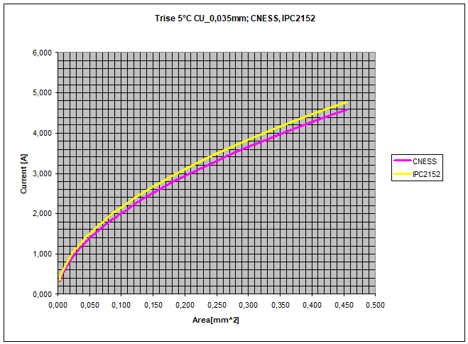 Figure: Comparison between CNES and IPC-2152 current rating at increase
Formulae for the three models
In the three models the temperature increment of tracks is calculated with respect to the initial temperature of the PCB when it is not powered.
Current rating and cross sectional area are calculated in the three models by using the following formulae:
Current rating [I in Amp]
Cross sectional area of tracks [A in mm2]
Temperature increment of tracks [ΔT in °C].
Constants k0, k1, m0, m1. The values of the constants are specified in the paragraphs describing each model.
Conversion factor mm2 to mils2 c1=1550.
Formula for current rating:
![]() Formula for cross sectional area:
Formula for cross sectional area:
![]()
Example of current rating
Using the mathematical model of IPC-2152 specified in clause D.2, to carry a current of 1 A and to maintain a temperature increment of 5 °C, a track of as-manufactured thickness of 25 µm (as-designed thickness of 35 µm, as per Table 71) should have an as-manufactured track width of 925 µm (as-designed width of 975 µm, as per Table 73).
Track current rating computation based on IPC-2152
The IPC-2152 is the most comprehensive standard for the computation of the track current rating. It includes track sizing charts for vacuum or space environment, for several PCB thicknesses and for several copper plane thicknesses in SI (metric) and Imperial (inch) units. This standard allows to accurately calculate the current rating of a track from cross sectional area and the temperature rising of the track. However no derating are applied to take into account the complexity of the PCB.
The model presented in this clause is based on a curve fitting performed on Figure 5-14 of chapter 5.2.2. of IPC-2152.
The model is valid for a range up to 30 A and up to 100°C temperature increment with respect to an initial PCB temperature of 25°C when not powered.
Current rating and cross sectional area are calculated as per the formula in clause D.1.2 with the following constants:
k0 = 0,0756
k1 = 0,4375
m0 = 0,5000
m1 = 0,0301
Example charts based on this model are shown in Figure D-2 to Figure D-7.
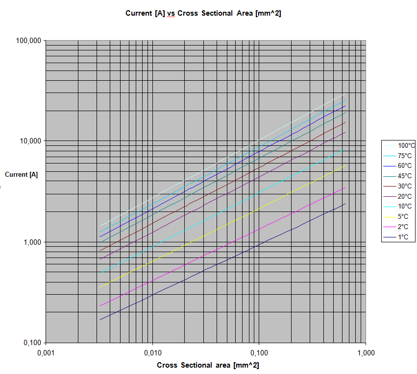 Figure: IPC-2152: Current rating [A] vs cross sectional area [mm2] in double log scale
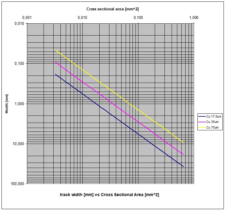 Figure: IPC-2152: Track width [mm] vs cross sectional area [mm2 ]
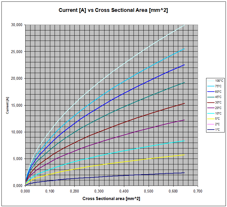 Figure: IPC-2152: Current rating based on Figure D-2, range 0-25 A
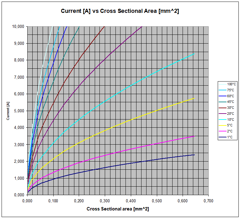 Figure: IPC-2152: Current rating based on Figure D-2, range 0-10 A
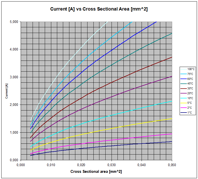 Figure: IPC-2152: Current rating based on Figure D-2, range 0-5 A
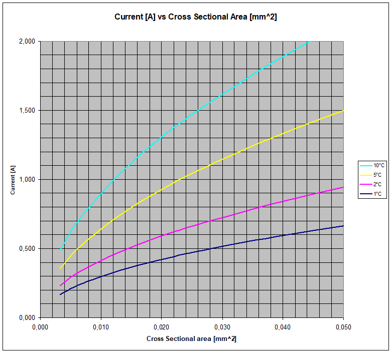 Figure: IPC-2152: Current rating based on Figure D-2, range 0-2 A
Track current rating computation based on CNES/QFT/IN.0113
The CNES current rating computation is based on the thermal model correlated to experimental data. The values obtained for current carrying capacity are about 10% more conservative with reference to those of IPC-2152.
The model does not apply derating to take into account the complexity of the PCB.
The model presented in this clause is based on a curve fitting performed on the data given in the table “Tableau de quelques valeurs particulieres, Intensite=f(largeur, ΔT)” on page 10 of CNES/QFT/IN.0113”.
The model is derived from experimental data ranging up to 8 A and up to 100°C temperature increment with respect to an initial PCB temperature of 25°C when not powered.
Current rating and cross sectional area are calculated as per the formula in clause D.1.2 with the following constants:
k0= 0,0594
k1= 0,4800
m0= 0,5420
m1= 0,0034
Example charts based on this model are shown in Figure D-8 to Figure D-13.
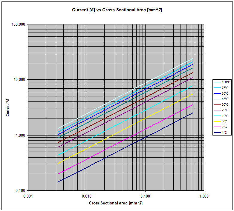 Figure: CNES/QFT/IN.0113: Current rating [A] vs cross sectional area [mm2] in double log scale
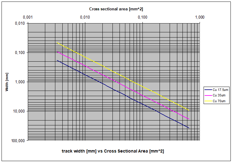 Figure: CNES/QFT/IN.0113: Track width [mm] vs cross sectional area [mm2]
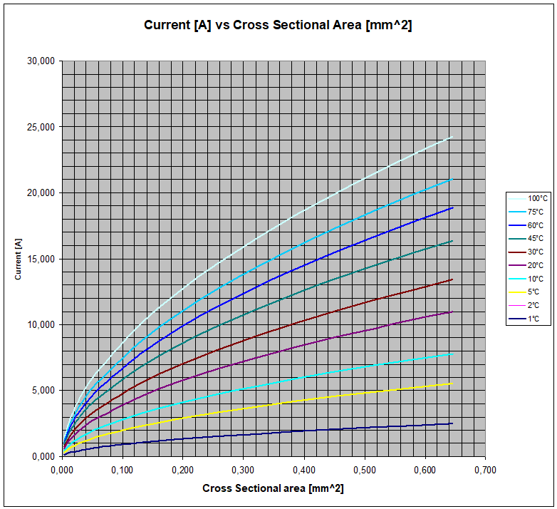 Figure: CNES/QFT/IN.0113: Current rating based on Figure D-8, range 0-25 A
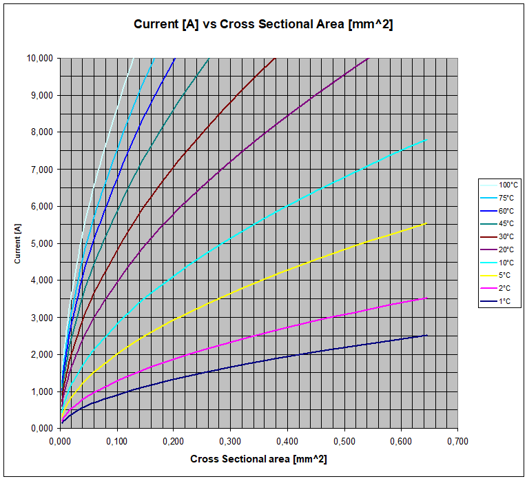 Figure: CNES/QFT/IN.0113: Current rating based on Figure D-8, range 0-10 A
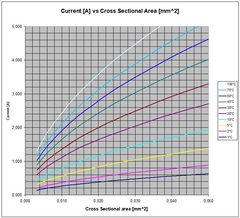 Figure: CNES/QFT/IN.0113: Current rating based on Figure D-8, range 0-5 A
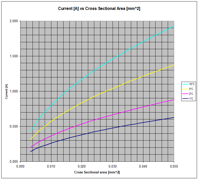 Figure: CNES/QFT/IN.0113: Current rating based on Figure D-8, range 0-2 A
Track current rating computation based on IPC-2221A
The model presented in this clause is based on a curve fitting performed on figure C for internal conductors of Figure 6-4 of IPC-2221A.
IPC-2221A is the most conservative method of the three methods defined Annex D. Derating is not used in this model.
The current rating is calculated with the following conditions:
I<0,7A for Trise 1 °C
I<0,9A for Trise 2 °C
I<1,0A for Trise 5 °C
I<1,2A for Trise 10 °C
- Within these conditions the current rating is about 70% of the current rating calculated with IPC-2152.
Current rating and cross sectional area are calculated as per the formula in the clause D.1.2 with the following constants:
k0 = 0,0240
k1 = 0,4393
m0 = 0,7252
m1 = 0,0002
Example charts based on this model are shown in Figure D-14 to Figure D-19.
 Figure: IPC-2221A: Current rating [A] vs cross sectional area [mm2] in double log scale
 Figure: IPC-2221A: Track width [mm] vs cross sectional area [mm2]
 Figure: IPC-2221A: Current rating based on Figure D-14, range 0-25 A
 Figure: IPC-2221A: Current rating based on Figure D-14, range 0-10 A
 Figure: IPC-2221A: Current rating based on Figure D-14, range 0-5 A
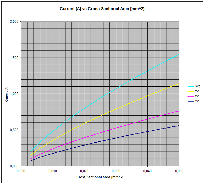 Figure: IPC-2221A: Current rating based on Figure D-14, range 0-2 A
ANNEX(informative)Example of calculation of PTH pad dimensions
Two examples of calculations of PTH pad dimensions are shown below. These calculations shown in Figure E-1 and Figure E-2 are specific for the PCB manufacturer as specified in the PID and depend on the complexity of the PCB designs.
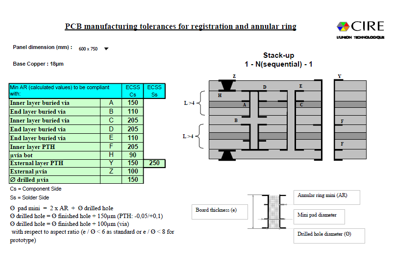 Figure: PCB manufacturing tolerances for registration and annular ring for HDI PCB
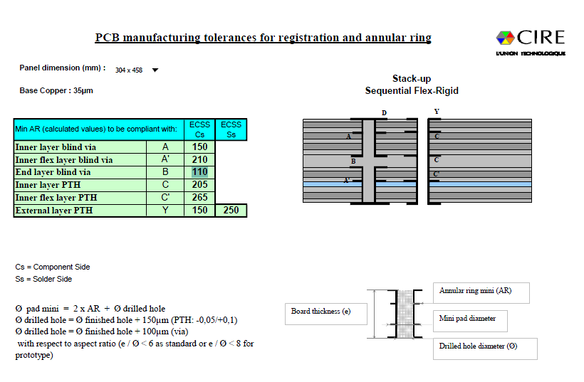 Figure: PCB manufacturing tolerances for registration and annular ring for rigid-flex sequential PCB
ANNEX(informative) Prevention of resin starvation and cracks
Prevention of resin cracks.
Under some conditions, cracks can develop in the laminate resin. They are more likely to appear:
In brittle resin types;
In locations with only resin and no reinforcement, such as openings in thick ground planes;
If the resin is mechanically stressed by drilling or routing.
The cause for the cracking can be mechanical impact or volume shrinkage during curing of the prepreg. Once a crack is formed, it can propagate into the laminate. The board manufacturing process can influence the formation of cracks. Design precautions to reduce the risk of crack formation include the following measures:
Avoid large volumes of resin without prepreg reinforcement.
Heat sinks often include large volumes of resin that can increase the risk of cracks. To avoid this, prepreg inserts in openings can be used.
Avoid low pressure areas due to opposite openings in superimposed copper layers.
Keep non-functional pads in planes.
Review the selection of material with PCB manufacturer.
Prepreg with filled resin can provide improved mechanical properties.
Prevention of resin starvation
Resin starvation is defined as a condition of insufficient resin to completely wet the glass reinforcement and fill the space between fibres. To reduce the risk for resin starvation the following can be done:
Allow sufficient prepreg thickness to fill the space between the copper pattern. High profile copper features throughout the PCB layers, such as a pad stack or superimposed tracks, can cause high pressure during lamination and can squeeze resin locally out of the prepreg if insufficient resin is available. The PCB manufacturer can implement additional prepreg between 70 µm copper layers compared to 35 µm copper layers.
Removal of non-functional pads can reduce the risk of resin starvation (see requirement 7.5.1b.2).
Fill open areas in thick copper layers with a non-functional-copper pattern to reduce the amount of resin required for filling. This can also help improve the thickness uniformity of the board.
See IPC-2222A clause 9.1.4 which mentions resin starvation and cracks in a discussion of removal of non-functional pads.
ANNEX(informative)Example of MRR checklist
The following is an example of “MRR checklist” document.
|
Supplier Specification:
| |||
|
PCB Manufacturer
|
|
Project
|
|
|
Supplier Article or Reference No:
|
|
Issue/revision
|
|
|
Article title:
|
|
Issue/revision
|
|
|
Supplier purchase order No:
|
|
purchase order Date
|
|
|
Feature Set
|
|
|
|
|
Is this a new or a recurring design?
|
|
||
|
If recurring please define all changes made to data set since the last purchase or state none.
|
|
||
|
If recurring please reference ALL occurrence reports raised against previous procurements of this or state none.
|
|
||
|
Is the design fully compliant with ECSS-Q-ST-70-12?
|
|
||
|
If the design is not compliant to ECSS-Q-ST-70-12 please list all deviations.
|
|
||
|
Has method and position of identification marking been defined?
|
|
||
|
* Printed Circuit Board Manufacturer Declaration:
(To be completed by the PCB manufacturer) | |||
|
Supplier work order No:
|
|
work order date
|
|
|
If this is a recurring design please define all changes made to tooling or processing since the last purchase or state none.
|
|
||
|
Manufacturer’s PID (Process Identification Document):
| |
|
Approved PID Reference including issue and revision
|
|
|
Deviations to the Approved PID
|
|
|
Contract Review:
| |
|
Please confirm contract review has taken place and reference controlling procedure(s) used.
|
|
|
Please list any anomalies or deviations arising from the contract review or state none.
|
|
|
Design:
| |||||
|
Have any changes to the provided data been requested following design rule checking (DRC)?
|
|
||||
|
Please list all changes and provide references below
| |||||
|
Reference of requesting e-mail (date, from, to)
|
Reference of supplier’s agreement (date, from, to)
|
Comments
|
Actions arising
| ||
|
Have all non-functional pads been kept?
|
|
||||
|
Has coupon sample data been included in the data pack?
|
|
||||
|
Has IST coupon sample data been included in the data pack?
|
|
||||
|
Has the position and quantity of coupon sample been agreed with supplier?
|
|
||||
|
Technical Review:
| |||
|
Please advise the base laminate and prepreg references to be used in fulfilment of this order.
|
|
||
|
Is there an extended lead time in procuring these materials?
|
|
||
|
Has this combination of materials been utilised on supplier’s flight product previously?
|
|
||
|
Is the stack-up of materials symmetrical for each pressing cycle?
|
|
||
|
How many press cycles lamination – drilling cycles will be required in the manufacture of this design?
|
|
||
|
Is the copper weight even on both sides of the laminate?
|
|
||
|
Are the copper weights with the range previously supplied for supplier’s flight products?
|
|
||
|
Are there two plies of glass present between every conductive layer – laminate and prepreg?
|
|
||
|
Where prepreg is intended to be used to backfill vias, is the resin content and board geometry suitable to support this?
|
|
||
|
For flex rigid only, is the process open or closed window?
|
|
||
|
How many flexible laminate layers are included in the design?
|
|
||
|
Risks identified from the technical review
|
Risk Rating
|
Risk Parameters requiring control
| |
|
Additional risks:
| |||
|
Have any additional risks to the manufacture of this product been identified
|
|
||
|
Additional risk identified |
Risk Rating
|
Risk Parameters requiring control
| |
|
Manufacturer Completing Signature:
| |
|
Position
|
Print Name; Sign and Date
|
|
Supplier Technical Authority review:
| |
|
Is the supplier technical authority in agreement with the risks identified and the rating applied by the manufacturer?
|
|
|
If no provide details of dis-agreement.
|
|
|
Have any additional risks been identified by the TA as a result of this review?
|
|
|
If yes give details.
|
|
|
Supplier Technical Authority Recommendations:
| |
|
Recommendation
|
Print Name, Sign and Date
|
|
Low to intermediate levels of risk 1 - 2, manufacture may continue without project counter-signature.
|
|
|
Medium levels of risk 3 - 4, risks to be entered in project risk register.
|
|
|
High risk 5, continuation against recommendation of supplier technical authority.
|
|
|
Authorising Signatures:
| |
|
Entity
|
Print Name, Sign and Date
|
|
Supplier Technical Authority
|
|
|
Supplier project manager (medium and high risk only)
|
|
Bibliography
|
ECSS-S-ST-00
|
ECSS system – Description, implementation and general requirements
|
|
ECSS-Q-ST-70-28
|
Space product assurance - Repair and modification of printed circuits board assemblies for space use
|
|
ASTM-B386-03, 2011
|
Standard Specification for Molybdenum and Molybdenum Alloy Plate, Sheet, Strip, and Foil
|
|
IPC-2141, Mar 2004
|
Design Guide for High Speed Controlled Impedance Circuit Boards
|
|
IPC-2221A, May 2003
|
Generic standard on printed board design
|
|
IPC-2221B, Nov 2012
|
Generic standard on printed board design
|
|
IPC-2222A, Dec 2010
|
Sectional design standard for rigid organic printed boards
|
|
IPC-2223C, Nov 2011
|
Sectional design standard for flexible printed boards
|
|
IPC-2226, Apr 2003
|
Sectional design standard for high density interconnect boards
|
|
IPC-2251, Nov 2003
|
Design guide for the packaging of high speed electronic
|
|
IPC-2315, Jun 2000
|
Design guide for high density interconnects (HDI) and microvias
|
|
IPC-4104, May 1999
|
Specification for high density interconnect (HDI) and microvias materials
|
|
IPC-4121, Jan 2000
|
Guidelines for selecting core constructions for multilayer printed wiring board applications
|
|
IPC-4202A, Apr 2010
|
Flexible base dielectrics for use in flexible printed circuitry
|
|
IPC-4204A, Oct 2013
|
Flexible metal clad dielectrics for use in fabrication of flexible printed circuitry
|
|
IPC-7095C, Jan 2013
|
Design and assembly process implementation for BGAs
|
|
IPC-7351B, Jun 2010
|
Land pattern and calculator
|
|
IPC-CF-152B, Dec 1997
|
Composite Metallic Material Specification for Printed Wiring Boards
|
|
IPC-T-50K, 2013
|
Terms and definitions for Interconnecting and packaging electronic circuits
|
|
RNC-CNES-Q-ST-70-101, version 8, Apr 2009
|
Spécifications de conception des cartes imprimées
|
|
CNES/QFT/IN.0113 rev 1, issue June 2000
|
Intensités admissibles en environnement spatial
|
|
D Cullen, G O’Brien, Proc. APEX 2004
|
“Implementation of Immersion Silver PCB Surface Finish In Compliance With Underwriters Laboratories”
|
See also Clause 2 for referenced normative IPC standards.