
Space product assurance
Manual soldering of high-reliability electrical connections
Foreword
This Standard is one of the series of ECSS Standards intended to be applied together for the management, engineering and product assurance in space projects and applications. ECSS is a cooperative effort of the European Space Agency, national space agencies and European industry associations for the purpose of developing and maintaining common standards. Requirements in this Standard are defined in terms of what shall be accomplished, rather than in terms of how to organize and perform the necessary work. This allows existing organizational structures and methods to be applied where they are effective, and for the structures and methods to evolve as necessary without rewriting the standards.
This Standard has been prepared by the ECSS-Q-ST-70-08 Working Group, reviewed by the ECSS Executive Secretariat and approved by the ECSS Technical Authority.
Disclaimer
ECSS does not provide any warranty whatsoever, whether expressed, implied, or statutory, including, but not limited to, any warranty of merchantability or fitness for a particular purpose or any warranty that the contents of the item are error-free. In no respect shall ECSS incur any liability for any damages, including, but not limited to, direct, indirect, special, or consequential damages arising out of, resulting from, or in any way connected to the use of this Standard, whether or not based upon warranty, business agreement, tort, or otherwise; whether or not injury was sustained by persons or property or otherwise; and whether or not loss was sustained from, or arose out of, the results of, the item, or any services that may be provided by ECSS.
Published by: ESA Requirements and Standards Division
ESTEC, ,
2200 AG Noordwijk
The
Copyright: 2009 © by the European Space Agency for the members of ECSS
Change log
|
ECSS-Q-70-08
|
First issue
|
|
ECSS-Q-ST-70-08C
|
Second issue
|
Introduction
The main part of this Standard is based on recommendations from the National Aeronautics and Space Administration and European soldering technology experts. Modifications have been incorporated into the text to provide for the specific requirement of low–outgassing electrical systems which are required by scientific and application satellites. Other additions have been made in the light of recent technological advances and the results of verification test programmes. The methods and workmanship contained in this document are considered to be fully approved for normal spacecraft requirements.
Scope
This Standard defines the technical requirements and quality assurance provisions for the manufacture and verification of manually-soldered, high-reliability electrical connections.
The Standard defines acceptance and rejection criteria for high reliability manufacture of manually-soldered electrical connections intended to withstand normal terrestrial conditions and the vibrational g-loads and environment imposed by space flight.
The proper tools, correct materials, design and workmanship are covered by this document. Workmanship standards are included to permit discrimination between proper and improper work.
The assembly of surface-mount devices is covered in ECSS-Q-ST-70-38.
Requirements related to printed circuit boards are contained in ECSS-Q-ST-70-10 and ECSS-Q-ST-70-11.
Verification of manual soldering assemblies which are not described in this standard are performed by vibration and thermal cycling testing. The requirements for verification are given in this Standard.
This standard does not cover the qualification and acceptance of EQM and FM equipment with hand soldered connections.
The qualification and acceptance tests of equipment manufactured in accordance with this Standard are covered by ECSS-E-ST-10-03.
The mounting and supporting of components, terminals and conductors prescribed herein applies to assemblies designed to operate within the temperature limits of 55 C to +85 C.
For temperatures outside this normal range, special design, verification and qualification testing is performed to ensure the necessary environmental survival capability.
Special thermal heat sinks are applied to devices having high thermal dissipation (e.g. junction temperatures of 110 C, power transistors) in order to ensure that solder joints do not exceed 85 C.
This standard may be tailored for the specific characteristic and constrains of a space project in conformance with ECSS-S-ST-00.
Normative references
The following normative documents contain provisions which, through reference in this text, constitute provisions of this ECSS Standard. For dated references, subsequent amendments to, or revision of any of these publications do not apply, However, parties to agreements based on this ECSS Standard are encouraged to investigate the possibility of applying the more recent editions of the normative documents indicated below. For undated references, the latest edition of the publication referred to applies.
|
ECSS-S-ST-00-01
|
ECSS system - Glossary of terms
|
|
ECSS-Q-ST-10-09
|
Space product assurance - Nonconformance control system
|
|
ECSS-Q-ST-20
|
Space product assurance - Quality assurance
|
|
ECSS-Q-ST-70-02
|
Space product assurance - Thermal vacuum outgassing test for the screening of space materials
|
|
ECSS-Q-ST-70-10
|
Space product assurance - Qualification of printed circuit boards
|
|
ECSS-Q-ST-70-11
|
Space product assurance - Procurement of printed circuit boards
|
|
ECSS-Q-ST-70-28
|
Space product assurance - Repair and modification of printed circuit board assemblies for space use
|
|
ECSS-Q-ST-70-71
|
Space product assurance - Data for selection of space materials and processes
|
|
ESCC 23500
|
Requirements for lead materials and finishes for components for space application
|
|
EN 61340-5-1
|
Protection of electronic devices from electrostatic phenomena - General requirements
|
|
EN 61340-5-2
|
Protection of electronic devices from electrostatic phenomena – User guide
|
|
MIL-STD-883 Rev.G
|
Test methods and procedures for microelectronics
|
Terms, definitions and abbreviated terms
Terms from other standards
For the purpose of this Standard, the terms and definitions from ECSS-ST-00-01 apply.
For the purpose of this Standard, the following terms from ECSS-Q-ST-70-28 apply:
repair
rework
Terms specific to the present standard
approval authority
entity that reviews and accepts the verification programme, evaluating the test results and grants the final approval
base laminate
see “substrate”
bifurcated (split) terminal
terminal containing a slot or split in which wires or leads are placed before soldering
bit
removable heat store of a soldering iron
blister
delamination in a distinct local area or areas
bridging
build-up of solder or conformal coating between parts, component leads or base substrate forming an elevated path
See “fillet”.
clinched-lead termination
conductor or component lead which passes through a printed circuit board and is then bent to make contact with the printed circuit board pad
The clinched portion is not forced to lie flat on the pad and some innate spring back is desirable before this form of termination is soldered.
cold flow
movement of insulation, for example Teflon (PTFE), caused by pressure
cold solder joint
joint in which the solder has a blocky, wrinkled or piled-up appearance and shows signs of improper flow or wetting action
It can appear either shiny or dull, but not granular. The joint normally has abrupt lines of demarcation rather than a smooth, continuing fillet between the solder and the surfaces being joined. These lines are caused by either insufficient application of heat or the failure of an area of the surfaces being joined to reach soldering temperature
component
device which performs an electronic, electrical or electromechanical function and consists of one or more elements joined together and which cannot normally be disassembled without destruction
- 1 The terms component and part can be interchanged.
- 2 Transistors, integrated circuits, hybrids, capacitors.
component lead
solid wire which extends from and serves as a connection to a component
conductor
lead or wire, solid or stranded, or printed circuit patch serving as an electrical interconnection between terminations
conformal coating
thin protective coating which conforms to the configuration of the covered assembly
connection
electrical termination
contact angle
angle enclosed between half-planes, tangent to a liquid surface and a solid-liquid interface at their intersection
In particular, the contact angle of liquid solder in contact with a solid metal surface. An approximate value for this can be determined by shadow projection or other means, by measuring after the solder has solidified. The contact angle is always the angle inside the liquid
contamination
particles, liquids, gases, materials and micro-organisms which by their presence can disturb the performance of an item
corrosion
deterioration of a metal by chemical or electrochemical reaction with its environment
cracked solder joint
soldered connection which has fractured or broken within the solder
dewetting
condition in a soldered area in which the liquid solder has not adhered intimately, characterized by an abrupt boundary between solder and conductor, or solder and terminal/termination area
This is often seen as a dull surface with islands of thicker shiny solder.
disturbed solder joint
unsatisfactory connection resulting from relative motion between the conductor and termination during solidification of the solder
electrical connection
conductive connection in electrical or electronic circuits
eutectic alloy
alloy of two or more metals that has one distinct melting point
One eutectic solder is a tin-lead alloy containing 63 % Sn and 37 % Pb which melts at 183 C
fillet
smooth concave build-up of material between two surfaces
Example: A fillet of solder between a component lead and a solder pad or terminal, or a fillet of conformal coating material between a component and printed circuit board
flux
material which, during soldering, removes the oxide film, protects the surface from oxidation, and permits the solder to wet the surfaces to be joined
flux activity
property of a flux which allows the smallest contact angle between molten solder and a solid surface
See also “rosin”.
glass meniscus
glass fillet of a lead seal which occurs where an external lead leaves the package body
haloing
condition existing in the base laminate of a printed circuit board in the form of a light area around holes or other machined areas on or below the surface of the laminate
hook terminal
terminal formed in a hook shape
icicles
see “solder icicle”
interfacial connection
conductor which connects conductive patterns between opposite sides of a printed circuit board
Normally a plated-through hole.
lap joint
joining or fusing of two overlapping metal surfaces with solder without use of any other mechanical attachment or support
measling/measles
condition existing in the base laminate of printed circuit board in the form of discrete white spots or “crosses” below the surface of the base laminate, reflecting a separation of fibres in the glass cloth at the weave intersection
During soldering this can be caused by excessive heat.
multi-layer circuit board
product consisting of alternate laminates of printed circuit substrates and insulators, bonded together by simultaneous application of heat and pressure prior to drilling and plating holes for interconnections
See also “printed circuit board”.
pad
termination of a conducting surface on a printed circuit board to which leads are soldered to form electrical connections
These can be described as either functional, where an active track is terminated, or non-functional, where the pad is isolated.
pits
small holes or sharp depressions in the surface of solder
This can be caused by flux blow-out due to entrapment or overheating
plated-through hole
hole in which metal is deposited on the inside surface
- 1 Adapted from IEC Multilingual dictionary.
- 2 Also known as a supported hole. The configuration is used to provide additional mechanical strength to the soldered termination or to provide an electrical interconnection on a double-sided or multi-layer printed circuit board.
potting compound
compound, usually electrically non-conductive, used to encapsulate or as a filler between components, conductors or assemblies
printed circuit board (PCB)
product resulting from the process of selectively etching unwanted copper from one or both surfaces of a copper-clad insulating substrate to form a desired circuitry pattern which is subsequently solder- or gold-plated
The term printed circuit board covers the following families:
- single sided;
- double sided, rigid or flexible;
- multilayer, rigid or flex-rigid.
resin
natural substance that is usually transparent or translucent and yellowish to brown
Resins are formed in plant secretions and are soluble in organic solvents, but not water. This is a generic term, rosin being the specific term with regard to soldering (see "rosin").
resistance soldering
method of soldering by passing a current between two electrodes through the area to be soldered
rosin
natural resin obtained as the residue after removal of turpentine from the oleoresin of the pine tree, consisting mainly of abietic acid and related resin acids, the remainder being resin acid esters
It is non-corrosive and electrically non-conducting. Rosin is the basic constituent of the rosin flux family (see ISO EN 29454).
rosin-soldered joint
unsatisfactory connection which has entrapped rosin flux
selective plating
area of a plated circuit board that is designed to have a different plated finish than the rest of the board
Example: A gold-finished RF board that supports tin-lead terminations (land areas).
shield
metallic sheath surrounding one or more wires, cables, cable assemblies, or a combination of wires and cables that is used to prevent or reduce the transmission of electromagnetic energy to or from the enclosed conductors
The shield also includes an insulating jacket that can cover the metallic sheath
solder
non-ferrous fusible metallic alloy of two or more metals (usually tin and lead) used when melted to join or fuse metallic surfaces together and to provide a low resistance electrical path
solderability
property of a surface which allows it to be wetted by molten solder
Standard tests exist to assess the solderability of conductors. Surfaces are considered to have a “good solderability” if, following the procedures of this standard, solder wetting can be achieved within 3 seconds and dewetting does not occur before 8 seconds.
solder coating
surface coated with a thin, uniform layer of solder
solder-cup terminal
hollow, cylindrical terminal closed at one end to accommodate one or more conductors
solder icicle
conical peak or sharp point of solder usually formed by the premature cooling and solidification of solder upon removal of the heat sources
solder pad
termination area on a printed circuit conductor
soldering
process of joining metallic surfaces through the use of solder without direct fusion of the base metals
soldering time
time required for a surface to be wetted by solder under specified conditions
stress lines
three forms of stress lines can appear on a finished solder fillet:
lines or folds running parallel to the mounting surface usually denote excessive soldering times or temperatures and also rework. They are probably caused during soldering by differential expansions, i.e. between the printed circuit board substrate which expands a far greater distance than the metallic material of the joint
lines running perpendicular to the mounting surface are commonly caused when the soldering iron bit is removed too slowly from a liquid solder joint
lines running circumferentially around the mid section of the solder fillet caused by shrinkage during the last stage of solidification
stress relief
method or means to minimize stresses to the soldered termination or component
Generally in the form of a bend or service loop in a component lead, solid or stranded wire to provide relief from stress between terminations, as that caused, for instance by movement or thermal expansion
stud termination
upright conductor termination through a printed circuit board
substrate
supporting dielectric material upon which the elements of a circuit are deposited or installed
termination/terminal area
conductive surface on a printed circuit board used for making electrical connections
Also referred to as printed circuit pad, solder pad.
thermal shunt
device with good heat-dissipation characteristics used to conduct heat away from an article being soldered
tinning
coating of a surface with a uniform layer of solder before it is used in a soldered connection
tip
application surface at the end of the soldering-iron bit
turret terminal
round post-type grooved stud around which conductors are fastened before soldering
wetting
flow and adhesion of a liquid to a solid surface, characterized by smooth, even edges and low contact angle
wicking
flow of molten solder or cleaning solution by capillary action
Occurs when joining stranded wire; solder is drawn within the strands, but normally not visible on outer surface of strands. Wicking can also occur within the stress relief bend of a component lead.
wire
single metallic conductor of solid, or stranded, construction, designed to carry current in an electric circuit, but which does not have a metallic covering, sheath or shield
For this standard, “wire” refers to “insulated electric wire”.
Abbreviated terms
For the purpose of this Standard, the abbreviated terms from ECSS-S-ST-00-01 and the following apply:
|
Abbreviation
|
Meaning
|
|
AWG
|
American wire gauge
|
|
ETFE
|
ethylene tetrafluoroethylene
|
|
ESD
|
electrostatic discharge
|
|
FEP
|
fluorinated ethylene propylene
|
|
INH1
|
IEC 61190-1-3 (2002) flux designation: inorganic, high activation ( 2 % halide)
|
|
PCB
|
printed circuit board
|
|
PSD
|
power spectral density
|
|
PTFE
|
polytetrafluoroethylene
|
|
RF
|
radio frequency
|
|
Rg
|
resistance to ground
|
|
Rs
|
surface resistance
|
|
ROH1
|
IEC 61190-1-3 (2002) flux designation: rosin, high activation ( 2 % halide)
|
|
ROL0
|
IEC 61190-1-3 (2002) flux designation: rosin, very low activation ( 0,01 % halide)
|
|
ROL1
|
IEC 61190-1-3 (2002) flux designation: rosin, low activation ( 0,15 % halide)
|
|
r.m.s.
|
root-mean-square
|
|
SMT
|
surface mount technology
|
Principles of reliable soldered connections
The following are the general principles to ensure reliable manually-soldered connections:
Reliable soldered connections are achieved by using proper design, having control of tools, selecting the right materials, applying processes with precaution in a controlled work environment and taking into account inspection requirements.
The basic design concepts to ensure reliable connections and to avoid solder joint failure are as follows:
Stress relief is an inherent part of the design, which reduces detrimental thermal and mechanical stresses on the solder connections.
Where adequate stress relief is not possible, a method of solder-joint reinforcement is incorporated.
Materials are selected such that the mismatch of thermal expansion coefficients is a minimum at the constraint points in the component-mounting configuration.
Materials and processes which result in the formation of brittle intermetallics, such as soldering to gold using tin-lead alloy, are avoided.
The assembled substrates are designed to allow inspection.
Preparatory conditions
Calibration
Calibration status of tools and inspection equipments shall be verified according to clause 14.4.
Records of the calibration and verification of the tools and inspection equipments shall be maintained.
Facility cleanliness
Personnel facilities shall be separated from the soldering areas.
Example: Washrooms, eating areas, smoking facilities.
Furniture shall be arranged to allow thorough cleaning of the floor.
Areas used for soldering shall be kept free from contaminants.
Loose material such as dirt, dust, solder particles, oil or clipped wires can contaminate soldered connections.
Working areas shall be kept free from any tools or equipment not used for the current task.
Working surfaces shall be covered with an easily-cleaned hard top or have a replaceable surface of clean, non-corrosive, silicone-free paper.
Tools used during soldering operations shall be free of visible contaminant.
Excess lubricants shall be removed from tools before soldering starts.
Environmental conditions
The soldering area shall have a controlled environment to limit the entry of contaminants.
It is good practice to solder in a clean room (see ISO 14644-1).
Areas used for assembly or cleaning of parts and areas where toxic or volatile vapours are generated or released shall include a local air extraction system.
The room temperature of the facility shall be maintained at 22 C ± 3 C.
The relative humidity at room temperature of the facility shall be maintained at 55 % ± 15 %.
The soldering area shall not be exposed to draughts.
Air shall be supplied to the room through a filtering system that provides a positive pressure difference with respect to adjacent rooms.
Lighting requirements
Lighting intensity shall be a minimum of 1080 lux on the work surface.
At least 90 % of the work area shall be without shadows or severe reflections.
Precautions against static discharges
General
An ESD Control Program in accordance with EN 61340-5-1 and EN 61340-5-2 shall be developed and implemented by the supplier.
Electrostatic sensitive components shall be prepared, mounted, soldered and cleaned in an ESD protected area.
Electrostatic sensitive components shall be kept as shipped (e.g. in anti-static tubes or foam) until assembly preparation.
Containers for ESD sensitive components shall be so labelled.
Precautions against ESD during manufacturing
The working bench shall have a static dissipative top with surface resistance (Rs) in the range 1 104 Ω to 1 1010 Ω.
The working bench shall have a static dissipative top resistance to ESD protected area ground (Rg) in the range 7,5 105 Ω to 1 109 Ω.
A wrist strap having a resistance to ESD protected area ground (Rg) in the range 7,5 105 Ω to 3,5 107 Ω shall be worn by the operator.
Seating shall have static dissipative surfaces with resistance to ESD protected area ground (Rg) less than 1 1010 Ω.
These measures prevent the build-up of static charges and avoid potential differences by keeping personnel, equipment and device leads at the same electrical potential, i.e. ground.
Powered equipment at the work station shall be grounded.
The normal value of the resistance between the tip of the soldering system and the ground of the ESD protected area does not exceed 5 Ω. The measurement is generally performed at soldering temperature.
A ground-fault circuit interrupter shall be installed.
Protective clothing shall be made from static dissipative material.
Gloves and finger cots shall be made from static dissipative material.
Tools, such as mounting aids, and consumables, masking tape, are expected to be conductive or static dissipative.
Paperwork accompanying ESD sensitive components shall be contained in static dissipative bags or envelopes.
Example of accompanying paperwork are traveller logs, drawings and instructions.
Paperwork shall not come into contact with ESD sensitive components.
Ionised air in presence of high voltage or RF shall not be used.
Static charges on isolated parts or tooling can be dissipated using ionised air.
Protective Packaging and ESD Protection
All ESD-sensitive items shall be contained within ESD-protective containers for movement between and within ESD-protected areas.
ESD protective packaging shall display ESD warning signs.
If the packaging is not ESD safe, it shall be labelled accordingly.
The objective of ESD protection is to prevent ESD to the item contained within, to allow for dissipation of charge, and to prevent charging of the ESDS item by an external electrostatic field.
A container shall provide for mechanical and ESD protection whenever the ESD-sensitive electronic assembly is transported within a manufacturing plant or during shipment to external destinations.
The container shall provide:
- an outer shell that provides adequate mechanical protection for the contents;
- foam or bubble wrap shock absorbing liners that have static shielding covers;
- a shielding package for the ESD sensitive contents. Pink-Polyethylene (pink-poly) bags, film, bubble wrap or foam near any ESD-sensitive item or within an ESD protected area shall not be used.
Pink-polyethylene provides little protection against ESD events and voltage fields and is a contamination source. The preferred alternative is the metallized static-shielding bag.
Packing and filler materials
Shipping popcorn, foam liners and polystyrene foam shall not be used near ESD-sensitive items unless shielding overwrap protects them.
Equipment and tools
General
New equipments and tools shall be inspected to ensure that they are not defective prior to use.
Brushes
Medium-stiff natural- or synthetic bristle, ESD-safe, brushes shall be used for cleaning provided that they do not damage any surface to be cleaned or adjacent materials.
Brushes shall be cleaned in a solvent in accordance with clause 6.4.
Brushes shall not be damaged by the solvents used for PCB cleaning.
Wire brushes shall not be used.
Cutters and pliers
Cutting edge profiles and cutter usage shall be in accordance with Figure 51.
The cutter used for trimming conductor wire and component leads shall shear sharply, producing a clean, flat, smooth-cut surface along the entire cutting edge.
- 1 These measures minimize the transmission of mechanical and shock loads to delicate parts.
- 2 Smooth, long-nose pliers or tweezers can be used for attaching or removing conductor wires and component leads.
No twisting action shall occur during the cutting operation.
Cutting edges shall be checked for damage and maintained in a sharp condition.
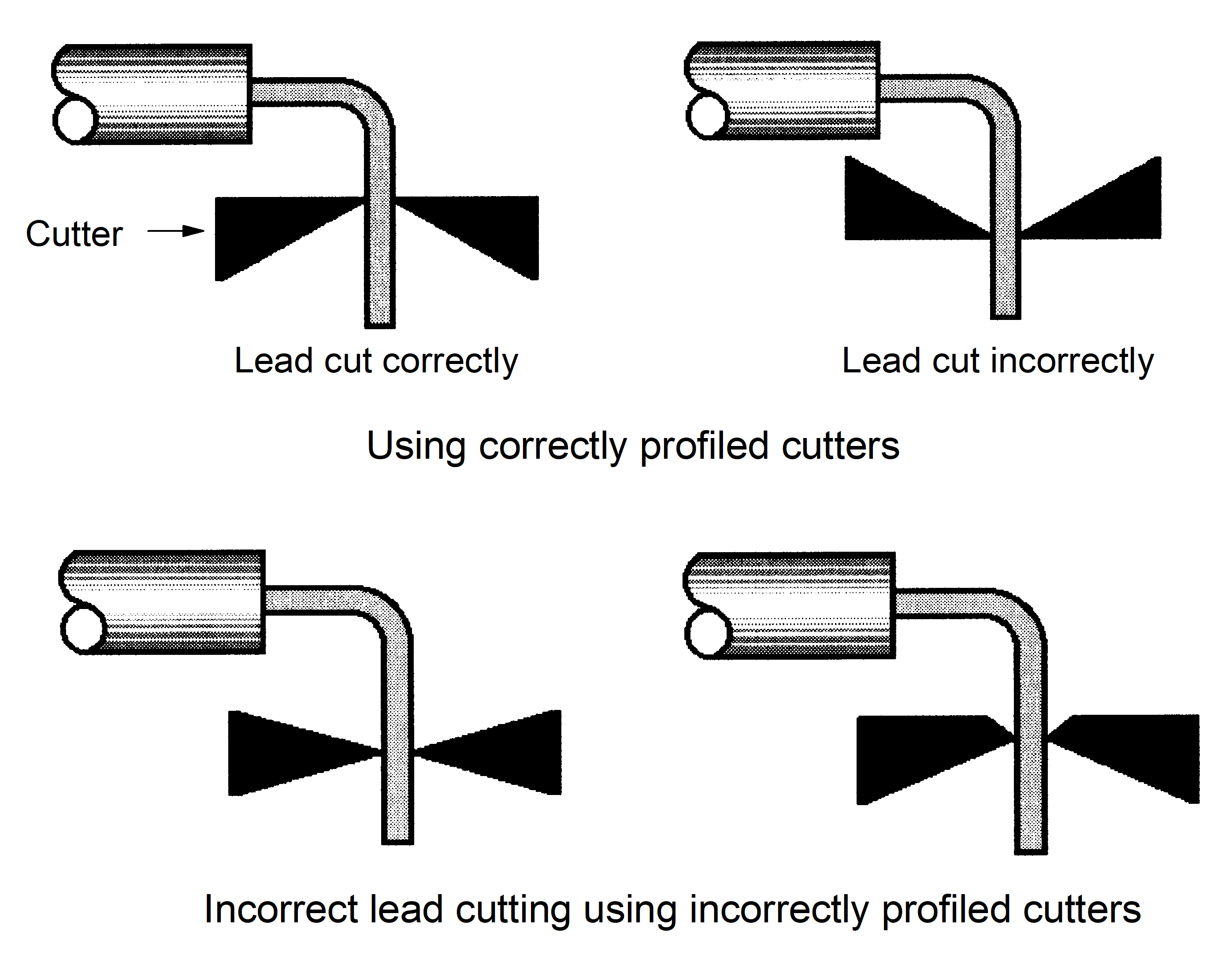 Figure 51: Profiles of correct and incorrect cutters for trimming leads
Bending tools
Bare component leads shall be bent or shaped using tools, including automatic bending tools, which do not cut, nick or damage the leads or insulation.
Components shall not be damaged by the bending process (see also clause 8.2).
It is good practice to use bending tools with polished finish. The preferred surface finish for shaping tools is hard chromium plating.
Bending tools shall have no sharp edges in contact with the component leads.
Clinching tools
Clinching tools shall not damage the surfaces of printed-circuit conductors, components or component leads.
Insulation strippers
Thermal strippers
The temperature of the stripper shall not burn, blister or cause excessive melting of the insulation.
- 1 Thermal insulation strippers can be used for wire insulation types susceptible to damage by mechanical strippers.
- 2 It is good practice to apply thermal strippers for use with AWG 22 and smaller wire sizes where there is a possibility of the wire stretching if a mechanical stripper is used.
- 3 Local air extraction units can be used during thermal stripping.
Precision mechanical cutting-type strippers
Mechanical strippers shall be of the following types:
- Automatic power-driven strippers with precision, factory-set, cutting and stripping dies and wire guards, or
- Precision-type hand strippers with accurately machined and factory-preset cutting heads.
Figure 52 shows some examples of unacceptable mechanical strippers.
Stripping tools or machines shall fit the size of the wire conductor.
It is good practice to mask off the die openings for wire sizes not in use.
The conductor shall not be twisted, ringed, nicked, cut or scored by the process.
 Figure 52 Examples of non-approved types of mechanical strippers
Enamel stripping
The enamel shall be removed by chemical or thermal means.
See also 6.7d.
The enamel may be removed by mechanical means provided that visual inspection using a minimum magnification of x40 is carried out to ensure that the conductor is undamaged.
Verification of stripping tools
Thermal and mechanical stripping tools shall be verified by sampling at the start of each production run.
Soldering irons and resistance soldering equipment
The size and shape of the soldering iron and bit shall not damage adjacent areas or connections during soldering operations.
Temperature-controlled soldering irons shall be used.
It is good practice to verify periodically the solder tip temperature.
Files shall not be used for dressing plated copper soldering-iron tips.
A selection of bit sizes and shapes appropriate to each soldering operation envisaged shall be available.
The soldering iron or resistance-heating electrode shall heat the joint area to the solder liquidus temperature in a time between 1 second and 2 seconds.
The soldering iron or resistance-heating electrode shall maintain the soldering temperature at the joint throughout the soldering operation.
Thermal shunts (see 5.6.8.3) shall be used to protect thermally-sensitive components.
For soldering of electronic components, the soldering-bit temperature shall be between 280 C and 350 C.
A soldering-bit temperature lower than 280 C may be used.
A soldering-bit temperature up to 380 C may be used for polyimide PCBs with heat sinks, wide tracks or ground planes.
A soldering bit temperature up to 360 C may be used for PCBs other than polyimide with heat sinks, wide tracks or ground planes.
A soldering iron holder shall be used.
It is good practice to use a cage-type holder that leaves the soldering-iron tip unsupported when a temperature-controlled soldering iron is used.
Soldering tools
General
The leads shall not be damaged during preparation and assembly.
Holding tools
Holding tools used as soldering aids shall not be wetted by the solder during the assembly.
Thermal shunts
Thermal shunts shall be used for the de-golding, pre-tinning and soldering of temperature-sensitive components.
An effective clamp-type thermal shunt can be constructed by sweating small copper bars into the jaws of an alligator clip.
The heat sink shall be used when the non-thermal sensitivity of the device cannot be demonstrated.
The thermal shunt shall not disturb the solder joint by mechanical interference.
Shunts shall be applied and removed without mechanically damaging the component or the assembly.
Shunts can be held in place by friction, spring tension, or any other means that does not damage the finish or insulation.
Anti-wicking tools
The conductor gauge sizes of the anti-wicking tools shall be marked on the tool.
Anti-wicking tools can be used for pre-tinning the stranded wires.
Materials selection
General
Material selection shall be performed in accordance with ECSS-Q-ST-70-71.
Components, subassemblies, assemblies and hardware for space flight applications shall not have tin finishes containing more than 97 % tin.
Electrical/electronic components identified as having plated or metallized external surfaces with a tin finish containing more than 97 % tin may be pretinned with a tin-lead solder in accordance with 6.2.2b.
Tin whisker mitigation (barrier methods such as coating or sleeving) is addressed in the framework of an NRB or Approval Authority.
Pretinning shall not degrade or damage the component.
See also 6.1c.
Subassemblies, assemblies and mounting hardware identified as having lead-free surfaces (plated or metallised) shall be protected by process or design to prevent metallic whisker formation in the expected end-use application/environment.
Operations carried out during degolding or pretinning shall not contravene the individual detailed specification for the component, PCB and terminations.
Solder
Form
For soldering, ribbon, wire and preforms shall be used provided that the alloy and flux meet the requirements of this standard.
For degolding and pretinning, solder alloys shall be supplied as ingots (without flux).
Composition
The solder alloy shall have a composition specified in Table 61.
- 1 See ISO 9453 for further details.
- 2 The solder alloy used depends on the application. See Annex Table B-1 for guidelines for the choice of solder type.
The solder alloy used for degolding and pretinning shall be 60 tin solder, 62 tin silver loaded or 63 tin solder.
Table 61: Chemical composition of spacecraft solders
|
ESA designation
|
Sn
|
Pb
|
In
|
Sb
|
Ag
|
Bi
|
Cu
|
Fe
|
Zn
|
Al
|
As
|
Cd
|
Other
|
|
63 tin solder
|
62,5-63,5
|
Rem.
|
-
|
0,05
|
-
|
0,10
|
0,05
|
0,02
|
0,001
|
0,001
|
0,03
|
0,002
|
0,08
|
|
62 tin silver loaded
|
61,5-62,5
|
Rem.
|
-
|
0,05
|
1,8-2,2
|
0,10
|
0,05
|
0,02
|
0,001
|
0,001
|
0,03
|
0,002
|
0,08
|
|
60 tin solder
|
59,5-61,5
|
Rem.
|
-
|
0,05
|
-
|
0,10
|
0,05
|
0,02
|
0,001
|
0,001
|
0,03
|
0,002
|
0,08
|
|
96 tin solder
|
Rem.
|
0,10
|
-
|
0,05
|
3,5-4,0
|
0,10
|
0,05
|
0,02
|
0,001
|
0,001
|
0,03
|
0,002
|
0,08
|
|
10 tin lead
|
9,0-10,5
|
Rem.
|
-
|
0,05
|
-
|
0,10
|
0,05
|
0,02
|
0,001
|
0,001
|
0,03
|
0,002
|
0,08
|
Flux
Rosin-based fluxes
Fluxes shall be selected in accordance with Table 62.
The preferred flux standard is IEC 61190-1-3 (2002).
For the pretinning of component leads, metallised terminations and terminal posts mildly-activated, rosin-based fluxes (e.g. ROL1) shall be used.
When pretinning with mildly activated rosin-based flux does not give acceptable wetting, fully activated rosin-based fluxes (e.g. ROH1) may be used.
ROH1 flux is extremely aggressive and can cause corrosion and damage to electronic materials.
When pretinning with fully activated rosin-based flux does not give acceptable wetting, INH1 corrosive, water-soluble, acid flux may be used in accordance with clause 6.3.2.
Difficulties in pretinning can arise from poor solderability.
For assembly the following fluxes shall be selected:
- For normal assembly, use pure rosin flux.
Example: Pure rosin flux ROL0.
- When mildly-activated rosin flux is used, monitor the effectiveness of subsequent cleaning operations in accordance with clause 11.3.
Example: Mildly-activated rosin flux ROL1.
Fully activated rosin-based fluxes shall be stored separately from pure rosin fluxes and mildly-activated rosin fluxes.
Example: Fully-activated rosin flux ROH1.
Table 62: Fluxes
|
|
IEC 61190-1-3 (2002)
|
Equivalent designation from ISO 29454 (1994)
|
Nature
|
Nominal composition (Weight %)
|
|
Pretinning
| ||||
|
Normal wetting
|
ROL1
|
1.1.2.W or X
|
Rosin
|
< 0,15% halide
|
|
Difficult wetting
|
ROH1
|
1.1.2.Z
|
Rosin
|
2,0% halide
|
|
Very difficult wetting
|
INH1
|
|
Inorganic Water soluble
|
> 2,0% halide
|
|
Assembly
| ||||
|
Preferred
|
ROL0
|
1.1.1
|
Rosin
|
< 0,01% halide
|
|
Requiring cleanliness testing
|
ROL1
|
1.1.2.W or X
|
Rosin
|
< 0,15% halide
|
INH1 corrosive acid flux
INH1 flux residues shall be removed immediately after use in accordance with clause 11, before any further soldering operations.
This flux shall not be used where vapours or residues of spattered flux can come into contact with electrical insulation material.
INH1 flux shall be stored separately from pure rosin fluxes and mildly-activated rosin fluxes.
INH1 flux leaves residues that promote stress-corrosion cracking and general surface corrosion.
Application of flux
The quantity of flux used shall be such that the solder joint is in accordance with clause 12.
When flux-cored solder is used, it shall be positioned such that the flux flows and covers the components to be joined as the solder melts.
When an external liquid flux is used in conjunction with flux-cored solders, the fluxes shall be compatible.
When external flux is used, liquid flux shall be applied to the surfaces to be joined prior to the application of heat.
Solvents
Solvents for the removal of grease, oil, dirt, flux and flux residues shall be electrically non-conductive and non-corrosive.
Solvents shall not dissolve or degrade the quality of parts or materials.
Solvents shall not remove component identification markings.
Solvents shall be labelled.
Solvents shall be maintained in an uncontaminated condition.
Solvents showing visual evidence of contamination or decomposition shall not be used.
Solvents shall not be used such that dissolved flux residue contaminates electrical contact surfaces.
Examples of electrical contact surfaces are those in switches, potentiometers or connectors.
The following solvents shall be used for cleaning in soldering operations:
- ethyl alcohol, 99,5 % pure or 95 % pure by volume,
- isopropyl alcohol, 99 % pure,
- deionized water at a maximum temperature of 40 C is used for removing certain fluxes provided that the assembly is thoroughly dried directly after cleaning,
- any mixture of 6.4h.1 to 3.
Other solvents that pass a compatibility test programme agreed by the Approval authority may be used.
Water-based solvents containing saponifiers shall not be used.
Solvents shall be selected such that they dry completely.
Flexible insulation materials
Materials shall have low outgassing properties in accordance with ECSS-Q-ST-70-02.
The following flexible insulation materials may be used in a space environment:
- ETFE, FEP and PTFE.
- Polyolefin and Kynar® sleeving for heat-shrinkable wire terminations.
- Irradiated polyethylene, fluorinated resin and polyimide. PTFE materials shall not be heated above 250 C.
Poisonous gases can be liberated above this temperature.
Terminals
Materials
Terminals shall be made from one of the following materials:
- Bronze (copper/tin) alloys.
It is good practice to use bronze terminals.
- Brass (copper/zinc) alloys. When a brass terminal is used it shall be plated with a barrier layer of copper or nickel of 3 µm to 10 µm.
- 1 A barrier layer is necessary on brass items to prevent the diffusion, and subsequent surface oxidation, of zinc.
- 2 It is good practice to use a copper barrier layer on brass terminals because nickel is magnetic and can have a poor solderability.
Terminals shall be tin/lead coated with an alloy containing a maximum of 97 % tin.
Example: Hot-dipped or reflowed electro-deposited coatings.
Terminals with coatings on the mounting surface shall be rejected if the coatings loosen in subsequent soldering operations.
Tin-, silver- and gold-plated terminals
Terminals on PCBs shall not be tin, silver or gold plated.
Tin, silver or gold-plated finishes shall be replaced using one of the methods described in clause 7.2.
Shape of terminals
Bifurcated and turret terminals shall have ledges or grooves to allow both the accurate location of connecting wires and the flow of solder.
Wires
Wire shall be made from high-purity copper or copper alloy.
The wire shall have one of the following finishes:
Silver-coating.
Wire-drawn, fused pure tin.
Enamelled.
Wires shall be stripped of their insulation in accordance with clause 7.2.1.
When stripping the ends of enamel wires the complete removal of the enamel shall be verified by visual inspection.
Chemical stripping materials shall be completely neutralised and be cleaned such that there are no residues from the stripping, neutralizing, or cleaning steps.
The enamel shall not be visually contaminated by the stripping process.
PCBs
Boards
Boards shall be made of materials, and manufactured, according to the requirements of ECSS-Q-ST-70-10 and procured according to ECSS-Q-ST-70-11.
For non-plated-through holes, interfacial connections shall be made according to clause 8.2.2.
Gold finish on conductors
Gold-plated conductors shall not be soldered.
Degolding of conductors shall be in accordance with clause 7.2.3.
RF circuits with gold finishes can have their terminal pads selectively plated with a tin-lead finish, see ECSS-Q-ST-70-11.
Component lead finishes
Component lead finishes shall conform to the requirements of ESCC 23500.
ESCC 23500 is only applicable for procured components and the pre-assembly operations as de-golding and pre-tinning are out of its scope.
Adhesives (staking compounds and heat sinking), encapsulants and conformal coatings
Limited shelf life items shall be stored and controlled in accordance with the material manufacturer’s recommendations or in accordance with the manufacturer’s documented procedures for controlling shelf life and shelf life extensions where permitted.
Adhesives shall be dispensable, non-stringing, and have a reproducible dot profile after application.
The uncured (tack) strength shall be capable of holding devices in place during handling prior to cure.
Adhesives, encapsulants and conformal coatings shall be non-corrosive to devices and substrates.
No materials that emit acetic acid, ammonia, amines, hydrochloric acid and other acids shall be used.
Such compounds can cause stress-corrosion cracking of part leads.
The adhesives, encapsulants and conformal coatings used shall not damage substrate materials or attached devices.
- 1 The effects of some conformal coatings on the reliability of solder joints are described in ESA SP 1173.
- 2 Adhesion to fused tin-lead finishes is poor, see also ECSS-Q-ST-70-28.
Adhesives, encapsulants and conformal coatings shall conform with the outgassing requirements of ECSS-Q-ST-70-02, clause 7.
Shrinkage of resin during cure and repair shall not degrade the coated articles.
Materials covered by this clause shall be individually assessed in accordance with ECSS-Q-ST-70-71, clause 5.2.7 when flammability requirements are applicable.
Adhesives, encapsulants and conformal coatings shall be selected on the basis of their thermal conductivity and dielectric properties.
Some thermally conductive adhesives used to dissipate Joule heating are listed in ESA STM 265.
Stress relief of device leads shall not be reduced by the encapsulant or conformal coating.
- 1 This is particularly important at low service temperatures.
- 2 The coefficient of thermal expansion, glass transition temperature and modulus of adhesives used under devices for thermal reasons, for achieving stand-off heights or for mechanical support during vibration, can be considered to ensure that the additional stress put on the solder joints does not degrade the solder joint reliability.
Preparation for soldering
General
Tools
Operators shall use tools that are fit for the purpose and undamaged prior to use.
Components
The supplier shall ensure that degolding, pretinning and soldering conditions do not exceed the values given by the individual component data sheets.
Preparation of conductors, terminals and solder cups
Insulation removal
Stripping tools
Stripping tools or machines shall be in accordance with clause 5.6.6.
Damage to insulation
The remaining conductor insulation shall not be damaged by the insulation removal process.
Conductors with damaged insulation shall not be used.
- 1 Example: Insulation damage includes nicks, cuts, crushing and charring.
- 2 The operation of mechanical stripping tools can leave slight pressure markings in the remaining conductor insulation. This effect is considered to be normal.
The insulation material shall not be charred by thermal stripping.
Discoloration of the insulation material after thermal stripping is normal.
Damage to conductors
The conductor shall not be damaged by the insulation removal process.
Example: Conductor damage includes twisting, ringing, nicks, cuts or scores.
Part leads and other conductors that are reduced in cross-sectional area by the insulation removal process shall not be used.
Coated wires where the base material is exposed shall not be used.
Insulation clearance
Maximum clearance
The maximum insulation clearance, measured from the solder joint, shall be as stated in Table 71.
In the case of the assembly of coil winding wires, maximum insulation clearances may be exceeded provided that electrical clearances are maintained.
Minimum clearance
For PTFE-insulated wire, the minimum distance between the insulation and the solder fillet shall be 1 mm.
The minimum clearance distance for PTFE insulation accommodates cold flow.
The minimum insulation clearance shall not result in insulation imbedded in the solder joint.
The minimum insulation clearance shall not obscure the contour of the conductor at the termination end of the insulation.
Table 71: Clearances for insulation
|
Wire diameter(American Wire Gauge)
|
Conductor diameter, d (mm)
|
Insulation clearance (maximum)
|
|
32 to 24
|
0,200 to 0,510
|
4 × d
|
|
22 to 12
|
0,636 to 2,030
|
3 × d
|
|
10
|
2,565
|
2 × d
|
Surfaces to be soldered
Cleaning
Before assembly, devices, wire, terminal and connector contacts shall be visually examined for cleanliness, absence of oil films and freedom from tarnish or corrosion.
Conducting surfaces to be soldered shall be cleaned using solvents specified in clause 6.4.
Abrasives shall not be used for surface preparation except in the case of gold-plating on substrates and devices in accordance with clause 7.2.3.2.1.
Abrasives can include pumice, pumice-impregnated erasers and emery paper.
Wire lay
Disturbed lay in stranded-wire conductors shall be restored before soldering.
Restoration of the lay shall be done without contaminating the conductor.
Terminals and solder cups
Terminals and solder cup sizes shall be selected to match the size of conductors in accordance with the manufacturer’s data sheet.
The size of terminals or solder cups shall not be modified.
De-golding of gold-plated leads and terminals
General
Tin-lead alloy solders shall not be used to solder to gold.
Methods for degolding
Removal of gold from PCB conductors by mechanical abrasion
Removal of gold from PCB conductors by mechanical abrasion shall not be used for removing gold plating greater than 1 µm thick.
The gold plating shall be removed using a pumice-impregnated eraser.
Removal of gold from PCB conductors by mechanical abrasion shall not damage the substrate materials.
Removal of gold from PCB conductors by mechanical abrasion shall not impair the solderability of the conductor.
Removal of gold from PCB conductors by mechanical abrasion shall not reduce the thickness of the copper conductor.
It is good practice to design PCBs with selective plating to avoid the necessity to remove gold plating, see clause 6.8.2.
Solder baths
Solder baths used for degolding and pretinning shall be in accordance with Table 72.
Surface impurities shall be removed from the bath surface before use.
A controlled method shall be established and implemented for the replacement of solder baths, based on either:
- Contamination: Replace the solder bath alloy when the contamination limits given in Table 72 are exceeded, or
- Time: Establish a schedule of solder-bath replacement with justification of the replacement frequency.
Gold-plated component leads and terminals shall be dipped into solder bath 1 for between 2 seconds and 3 seconds.
The leads shall be pre-tinned in bath 2 in accordance with clause 7.2.6.
The component leads shall be allowed to cool before cleaning.
Solder cup method: to dissolve the gold plating
Solder shall be melted within the gold-plated solder cup.
The liquid solder dissolves the gold plating.
The liquid solder shall be wicked-out using stranded wire.
Solder iron method
Solder shall be melted onto the conductor using a heated soldering iron.
Solder shall be wicked-out using stranded wire.
Table 72: Solder baths for degolding and pretinning
|
|
Solder bath 1
|
Solder bath 2
|
|
Use
|
Gold dissolution
|
Pretinning
|
|
Temperature range (C)
|
250 to 280
|
210 to 280
|
|
Contamination limits (weight %)
|
Au < 1
|
Cu < 0,25; Au < 0,2; (Cu + Au) < 0,3; Zn, Al and Fe: Trace.
|
Constraints on degolding and pretinning methods
The maximum soldering rating of the component, stated by the manufacturer, shall not be exceeded.
Thermal shunts, in accordance with clause 5.6.8.3, may be used.
Components having glass-to-metal lead seals shall be preformed according to clause 5.6.4 before pre-tinning.
Liquid solder shall not come into contact with the component body or its glass meniscus.
The limit of the pretinned coating shall not be less than 0,75 mm from any lead-to-glass seal of the component package.
Pretinning of stranded wires
Solder baths
Solder baths for pretinning shall be in accordance with clause 7.2.3.
Stranded wires may also be pre-tinned by applying solder to the wire using a heated soldering-iron tip.
Solder bath method
The insulation shall be removed in accordance with clause 7.2.1.
Pure rosin flux shall be applied to the end of the strands.
The fluxed end of the wire shall be dipped into solder bath 2 for a time between 2 seconds and 3 seconds.
Pretinning promotes solderability and prevents untwisting or separation stranded wires.
Constraints on pretinning of stranded wires
Solder shall penetrate to the inner strands of stranded wire.
Solder shall not obscure the wire contour at the termination end of the insulation.
Anti-wicking tools in accordance with clause 5.6.8.4 may be used.
Pretinning shall not degrade the characteristics of the wire.
Flow of solder (wicking) beyond the insulation can reduce the flexibility of the wire.
The insulation shall not be damaged by the pretinning.
Flux shall be removed by means of a cleaning solvent, see clause 6.4.
Cleaning solvent shall not flow under the conductor insulation.
Application using a lint-free cloth can limit the flow of solvent.
Pre-tinning of component leads and solid-wire conductors
Solder bath method:
Solder baths for pretinning shall be in accordance with clause 7.2.3.
1. Component leads with unacceptable solderability in accordance with the component procurement specification and solid wires shall be pre-tinned by dipping into solder bath 2 (see Table 72) for a period between 2 seconds and 8 seconds.
- 1 It is good practice to observe an immersion period of between 3 seconds and 4 seconds.
- 2 A slow, vertical and smooth withdrawal of the component lead from the bath promotes an even coating.
The cross-sectional area of conductors shall not reduce by dissolution into the solder bath.
The component shall cool before cleaning.
Rapid cooling by contact with cleaning solvents can crack packages or glass-to-metal seals.
Soldering-iron method:
Solder shall be melted onto the conductor using a heated soldering iron.
Preparation of the soldering bit
Fit
The bit shall be fitted in accordance with the equipment manufacturer’s specification.
Maintenance
Oxidation products shall be removed from the bit.
Build up of oxidation products can reduce the ability of the tip to transfer heat.
Plated tips shall be examined for cracking.
Cracked platings allow the liquid solder to alloy with and erode the underlying copper, forming intermetallics which reduce heat transfer and lead to unacceptable joints.
Prior to examination, solder obscuring the surface shall be removed when the iron is hot by wiping the bit with moist, lint-free, sponge material.
Bits with cracked platings shall be removed from the soldering area.
Plated bits
Deposits shall be removed using a moist sponge.
Adherent deposits may be removed using fine abrasive paper (grain size 600).
The use of a file to remove the deposits is forbidden.
Tip in operation
The working surface of the tip shall be pretinned in accordance with clause 7.2.6.
Pretinning prevents oxidation of the bit.
Maintenance of resistance-type soldering electrodes
The surfaces of electrodes shall be kept free of contamination or corrosion.
Handling (work station)
ESD-sensitive components shall be handled in accordance with clause 5.5.
Metal surfaces to be soldered that show visible evidence of contamination shall be cleaned with a solvent specified in clause 6.4.
During assembly, component leads, terminals, wire ends and PCB termination areas shall not be touched with bare hands.
After final cleaning, personnel working with PCBs shall wear lint-free gloves or finger cots.
Storage (work station)
Components
Storage facilities shall protect components from contamination and damage.
Storage boxes and bags shall be made of materials which do not degrade the solderability of the components.
Storage materials shall not contain amines, amides, silicones, sulphur or polysulphides.
Packaging and containers for ESD-sensitive devices shall be in accordance with clause 5.5.
PCBs
PCBs shall be stored in accordance with ECSS-Q-ST-70-11, clause 7.1.
Materials requiring segregation
Solders not in accordance with clause 6.2 shall be removed from the work area.
Activated fluxes shall be stored in accordance with clause 6.3.1f.
Example: ROH1 flux.
Corrosive acid fluxes shall be stored in accordance with clause 6.3.2c.
Example: INH1 flux.
Solvents that do not conform to clause 6.4 shall be removed from the work area.
Example: Solvents contaminated with impurities such as inorganic acids.
Preparation of PCBs for soldering
Process
PCBs shall be Cleaned using solvent conforming to clause 6.4.
PCBs shall be demoisturized in accordance with clause 7.7.2.
Prepared PCBs shall be stored in accordance with clause 7.7.3.
Demoisturization methods
The oven temperature shall be between 90 C and 120 C.
It is good practice to follow the PCB manufacturer’s recommendations.
The process time shall be a minimum of 4 hours.
- 1 Long baking periods at higher temperatures can reduce the solderability of PCB terminations.
- 2 A vacuum bake method can be selected for temperatures less than 90 C.
Storage of prepared PCBs
The demoisturization process shall be carried out again according to clause 7.7.2 when prepared PCBs are stored in ambient conditions for more than 8 hours prior to soldering.
Dry nitrogen, dry air, vacuum or desiccants may be used to extend the storage period.
Mounting of components
General requirements
Introduction
Components shall be mounted parallel to the mounting surface.
Components shall be mounted in contact with the mounting surface.
Components may be mounted not more than 3,5 mm above the mounting surface, see Figure 81.
Materials used to support components shall meet the requirements of ECSS-Q-ST-70-71, clause 5.
Heavy components
Components weighing more than 5 g shall be supported by either of the following methods:
- adhesive compounds in accordance with clause 6.10, or
- mechanical methods.
For example: Lacing.
The support method shall not impose stresses that result in functional degradation or damage to the part or assembly.
The support method shall not impair stress relief designs.
Metal-case components
Metal-case components shall be electrically insulated using space-approved materials in accordance with ECSS-Q-ST-70-71, Annex C where they meet one of the following conditions:
- mounted over printed conductors;
- in contact with another metal-case component;
- in contact with a conductive material.
Metal-cased components shall not be mounted over soldered connections.
Component identification marks shall not be obscured by the insulation.
For example the serial numbers.
Glass-encased components
Glass-encased parts shall be enclosed with sleeving when epoxy material is used for staking, conformal coating or encapsulating.
Epoxy material cannot be applied directly to the glass.
Glass-encased components may be enclosed in resilient transparent sleeving or in heat-shrinkable sleeving.
Heating and shrinkage of sleeving can damage glass-encased components.
Stress relief of components with bendable leads
Stress relief shall be incorporated into:
- soldered leads and conductors,
- interfacial connections.
- 1 Stress relief provides freedom of movement for component leads or conductors between points of constraint.
- 2 Stresses can arise between points of constraint due to mechanical loading or temperature variations.
Stress relief methods, shown in Figure 82, Figure 85, Figure 810 and Figure 811, shall apply.
The assembly of TO-39, TO-59 and CKR-06 packages shall be performed in accordance with Figure 81 when assembled without stress relief.
Stress relief designs shall not damage the assembly.
Long lead lengths or large loops between constraint points can vibrate and damage the assembly.
Leads shall not be temporarily constrained against spring-back force during soldering.
Residual stresses are produced in the lead material or solder joint.
Solder fillets shall not impair stress relief bends.
CKR-06 and similar packages shall be adhesively staked in accordance with Figure 81.
The use a filler (silica powder) can prevent excessive flow of adhesive.
TO 39 and TO 59 packages may have an underfill as shown in Figure 81.
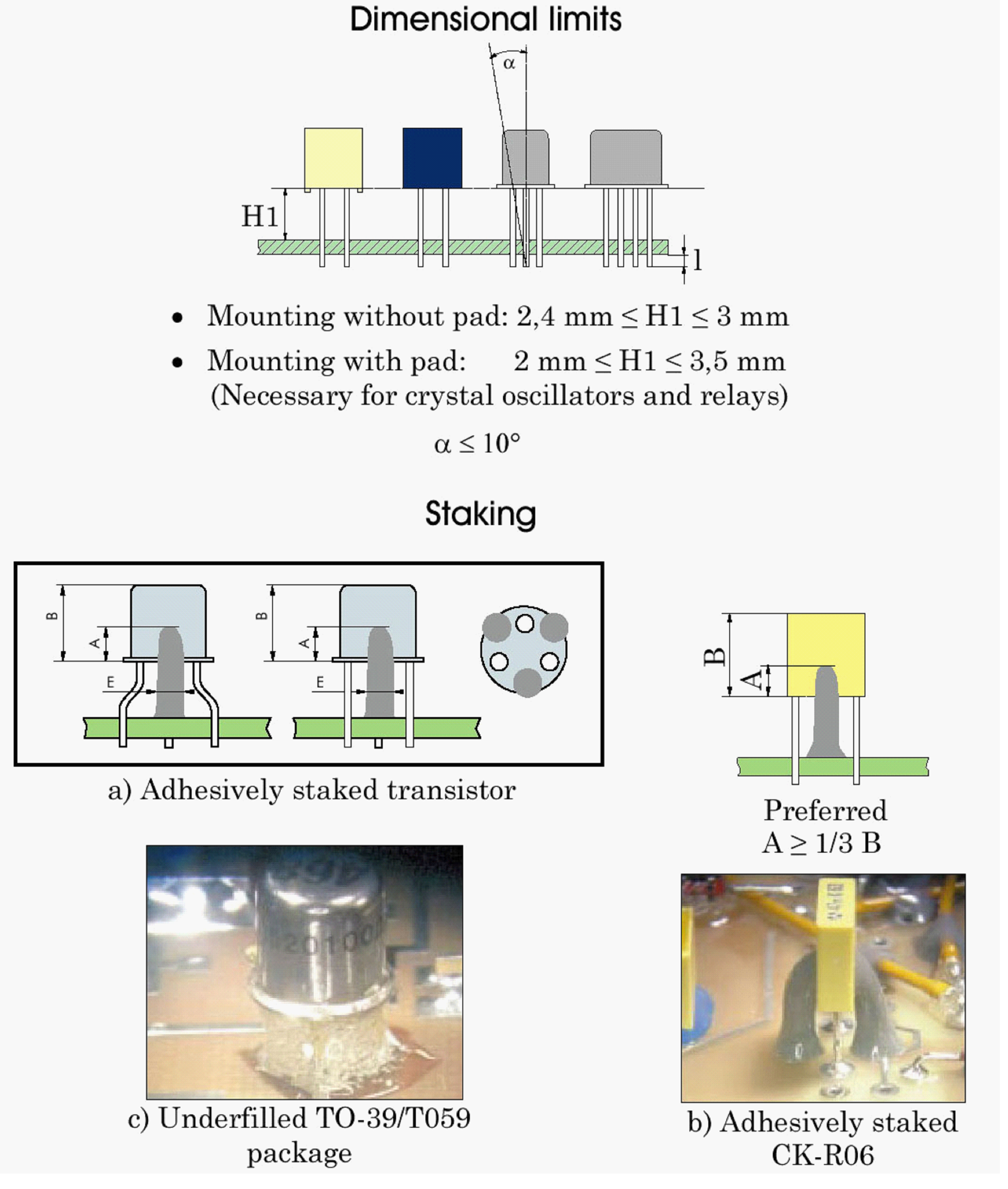 Figure 81: Assembly of underfilled TO-39 and TO-59, and adhesively staked CKR06
Stress relief of components with non-bendable leads
Stress relief for components with non-bendable leads mounted in contact with the PCB or adhesively bonded to the PCB shall use wire extensions, see Figure 83.
Bending can damage components when lead diameters are large or components have delicate seals or where lead-material composition makes bending impracticable.
DIP devices up to DIP 24 may be assembled without additional stress relief, provided that the tapered portions of the leads are clear of the component-side lands of the plated-through holes.
In order to achieve acceptable stand-off, a shim can be used.
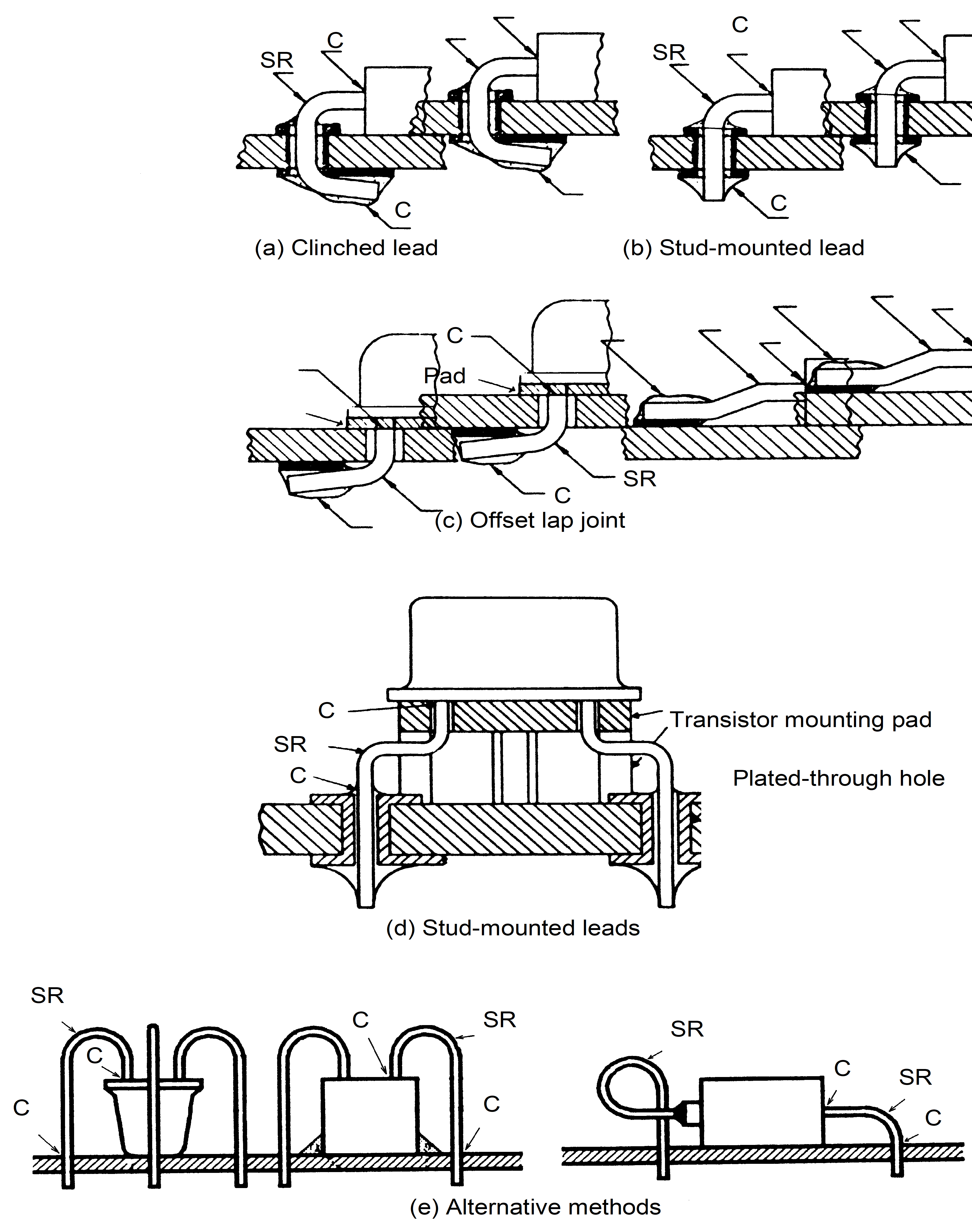 Figure 82: Methods for incorporating stress relief with components having bendable leads
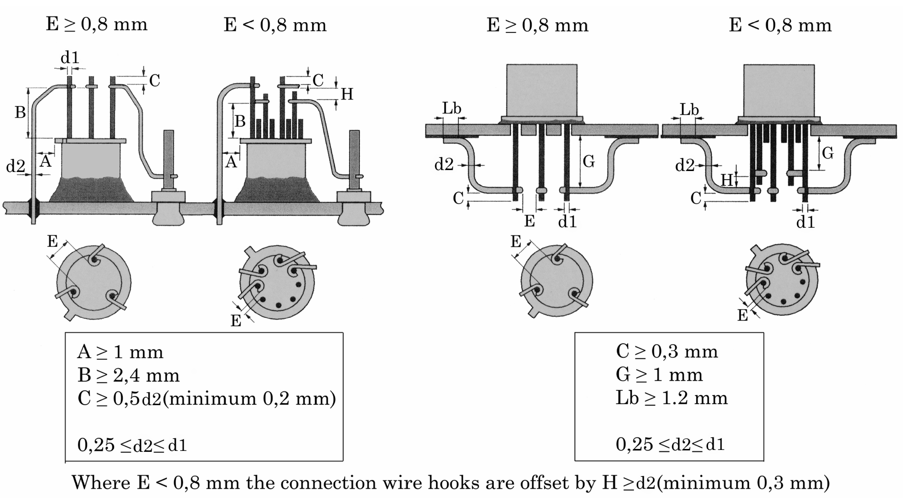 Figure 83: Methods for attaching wire extensions to non-bendable leads
Reinforced plated-through holes
Clause 6.8.1 shall apply for reinforced plated-through holes.
Lead and conductor cutting
Solder terminations shall not be cut after the soldering operation.
Component leads and wires are cut and shaped before soldering.
Solid hook-up wire
Solid hook-up wire shall be supported at intervals not exceeding 30 mm.
The support shall be provided by staking.
Location
Component bodies shall not be located in contact with soldered or welded terminations.
Conformal coating, cementing and encapsulation
Coatings and cementing compounds shall not bridge stress relief loops or bends at terminations in component leads or connecting wires.
Stress relief of device leads shall not be impaired by encapsulants or conformal coatings.
Lead bending requirements
General
During bending, component leads shall be supported to avoid axial stress and damage to seals or internal bonds.
The inside radius of a bend shall not be less than the lead diameter or ribbon thickness.
The distances between the bends and the end seals at either end of an axial component shall be similar.
The minimum distance from the bend to the end seal shall be two lead diameters for round leads and 0,50 mm for ribbon leads.
Where the component lead is welded the minimum distance to the bend shall be measured from the weld in accordance with Figure 84.
Example: Tantalum capacitors.
Bending tools shall not impinge on the weld.
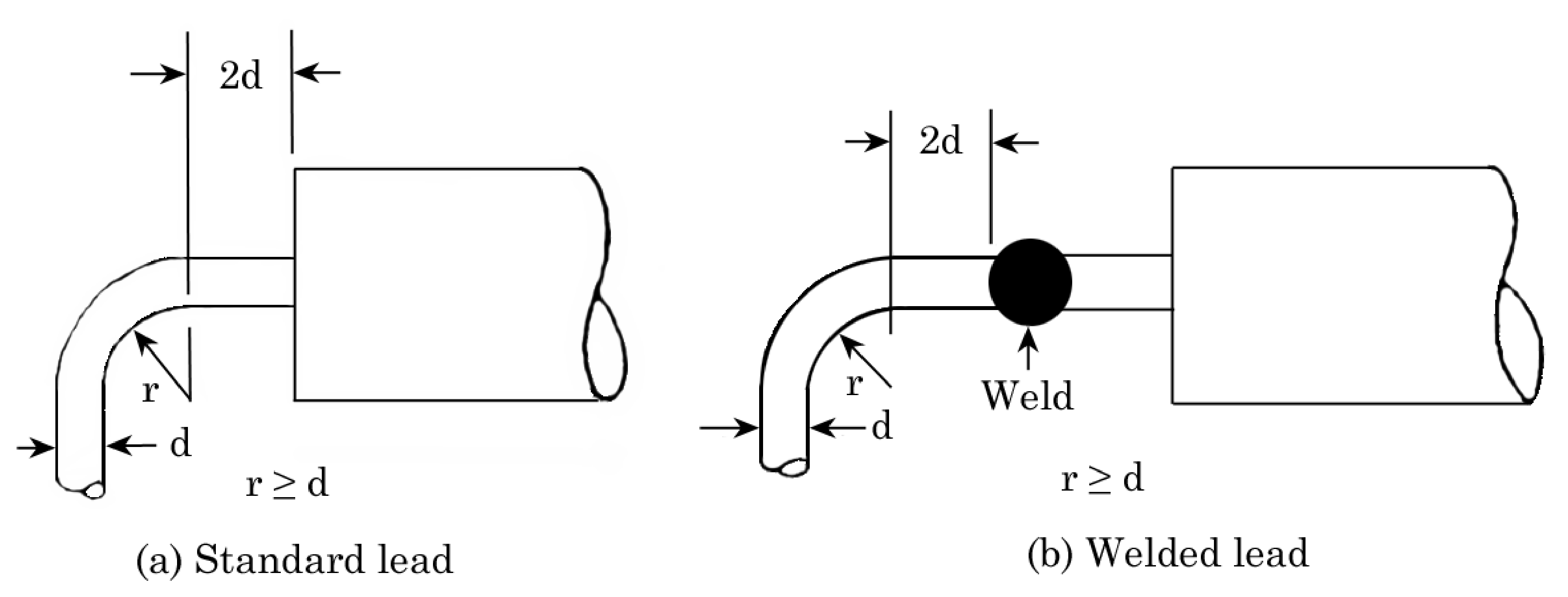 Figure 84: Minimum lead bend
Conductors terminating on both sides of a non-plated-through hole
Stress relief shall be provided in the component lead on both sides of the PCB in accordance with Figure 85 (a).
When a solid hook-up wire is used to interconnect solder terminations on opposite sides of a PCB, stress relief shall be provided in the wire between the two terminations in accordance with Figure 85 (b).
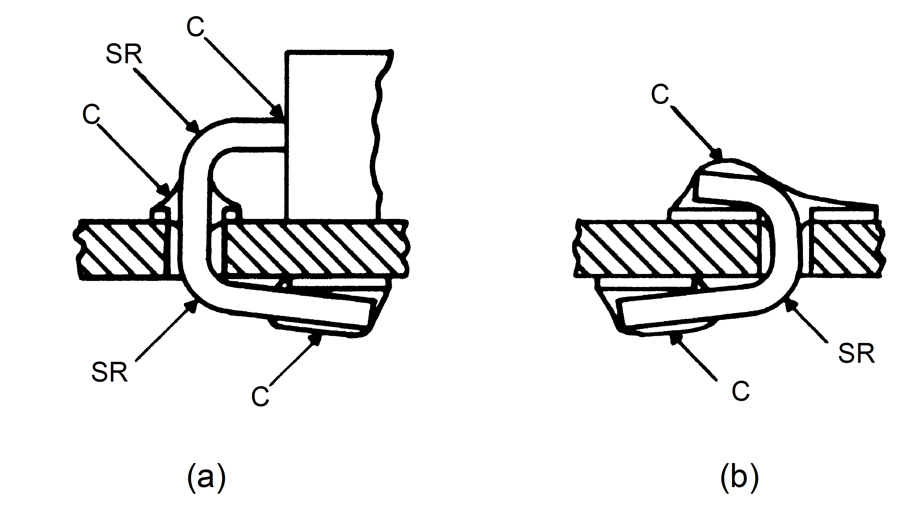 Figure 85: Leads with solder termination on both sides
Mounting of terminals to PCBs
Swage-type terminals, designed to have the terminal shoulder soldered to printed conductors, shall be secured to single-sided PCBs by a roll swage in accordance with Figure 86 (a).
Swage-type terminals that are mounted in a plated-through hole shall be secured to the PCB by an elliptical funnel swage in accordance with Figure 86 (b).
An elliptical funnel swage enables complete filling of the plated-through hole with solder.
The PCB shall not be damaged by the swaging process.
After swaging, the terminal shall be inspected for circumferential splits or cracks.
After swaging, the terminal shall be free from circumferential splits or cracks.
After swaging, the terminal may have a maximum of three radial splits or cracks, provided that the splits or cracks do not extend beyond the swaged area of the terminal and are a minimum of 90 apart.
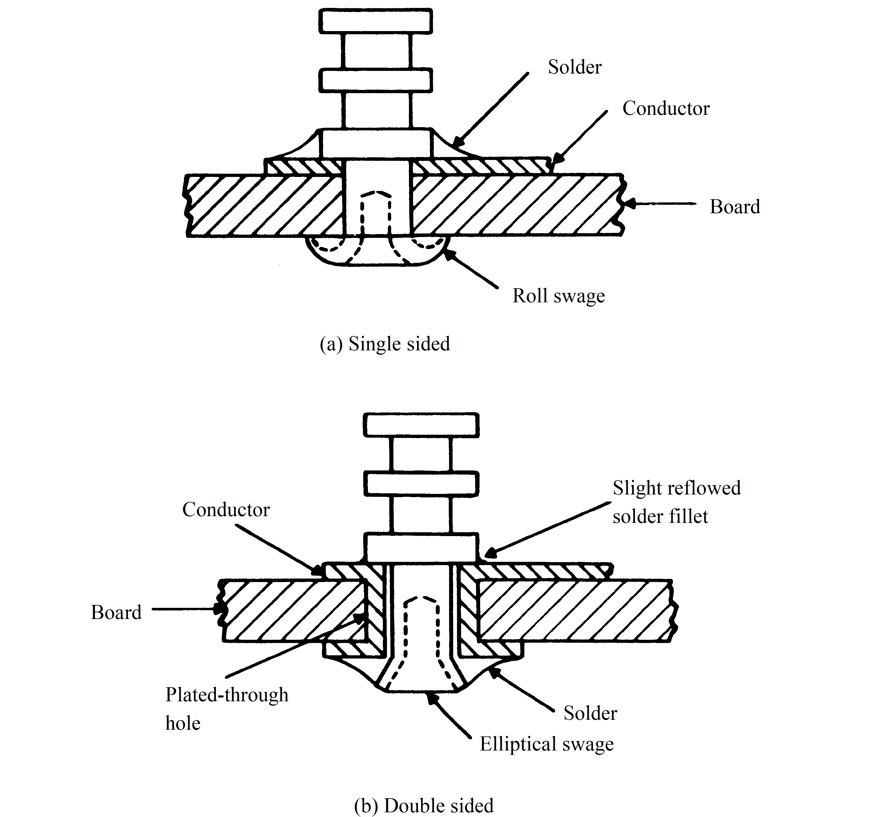 Figure 86: Types of terminal swaging
Lead attachment to PCBs
General
Solder terminations shall be visible for inspection after soldering.
Component leads shall be terminated to PCBs by clinch, stud or lapped terminations.
Clinched leads
Non-bendable leads shall not be clinched, see also clause 8.1.6.
Clinched leads terminating at a PCB pad shall be bent to make contact with the printed circuit conductors.
The clinched lead shall not extend beyond the edge of the conductor pattern, see Figure 87 and Figure 88.
The lead shall not be forced to lie flat at the bend radius, see Figure 87 and Figure 88.
Component leads can spring-back when clinched.
The soldered length shall comply with clauses 8.4.4 and 8.4.5.
Rounded termination areas shall be such that:
- the lead extends through and overlap the solder pad,
- the lead is bent in the direction of the longest dimension of the solder pad, and
- the area of the solder-pad permits a solder fillet to be formed.
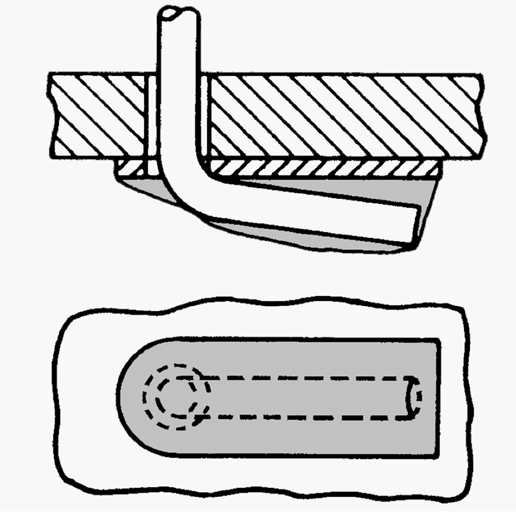 Figure 87: Clinched-lead terminations - unsupported holes
 Figure 88: Clinched lead terminations - plated through-holes
Stud leads
For unsupported holes, the cut stud leads shall protrude beyond the PCB surface by 1,5 mm ± 0,8 mm, see Figure 89 (a).
For plated-through hole less than 2,2 mm in length, the cut stud leads shall protrude beyond the PCB surface by 1,5 mm ± 0,8 mm, see Figure 89 (b).
For components with short leads and plated-through holes, greater than or equal to 2,2 mm in length, the protrusion may be zero, provided that the outline of the lead is visible, there is wetting between the lead and pad around the entire circumference and there is complete penetration of solder to the component side, see Figure 8-9 (c).
 Figure 89: Stud terminations
Lapped round leads
Round leads shall overlap the solder pad:
- Minimum overlap: Either 3,5 times the lead diameter or 1,3 mm, whichever is the greater.
- Maximum overlap: 5,5 times the lead diameter.
The distance from the cut end of the lead to the edge of the solder pad shall be more than 0,5 times the lead diameter.
No portion of the soldered lead termination shall project beyond the edges of the pad.
Lapped ribbon leads
Ribbon leads shall overlap the solder pad, see Figure 810 (b):
- Minimum overlap: Either 3 times the lead width or 1,3 mm, whichever is the greater.
- Maximum overlap: 5 times the lead width.
No portion of the soldered lead termination shall project beyond the edges of the pad.
The distance from the cut end of the lead to the edge of the solder pad shall be at least 0,25 mm.
One side of the lead may be flush with the edge of the solder pad.
Mounting of components to terminals
Components shall be mounted in accordance with clause 8.1.
Degree of wrap, routing and connection to terminals shall be in accordance with clause 9 and clause 10.
The lead length between the component and the terminals shall be similar at both ends, except where component package shapes dictate staggering.
Example: Top hat diodes with flanges.
Stress relief shall be provided in accordance with Figure 811.
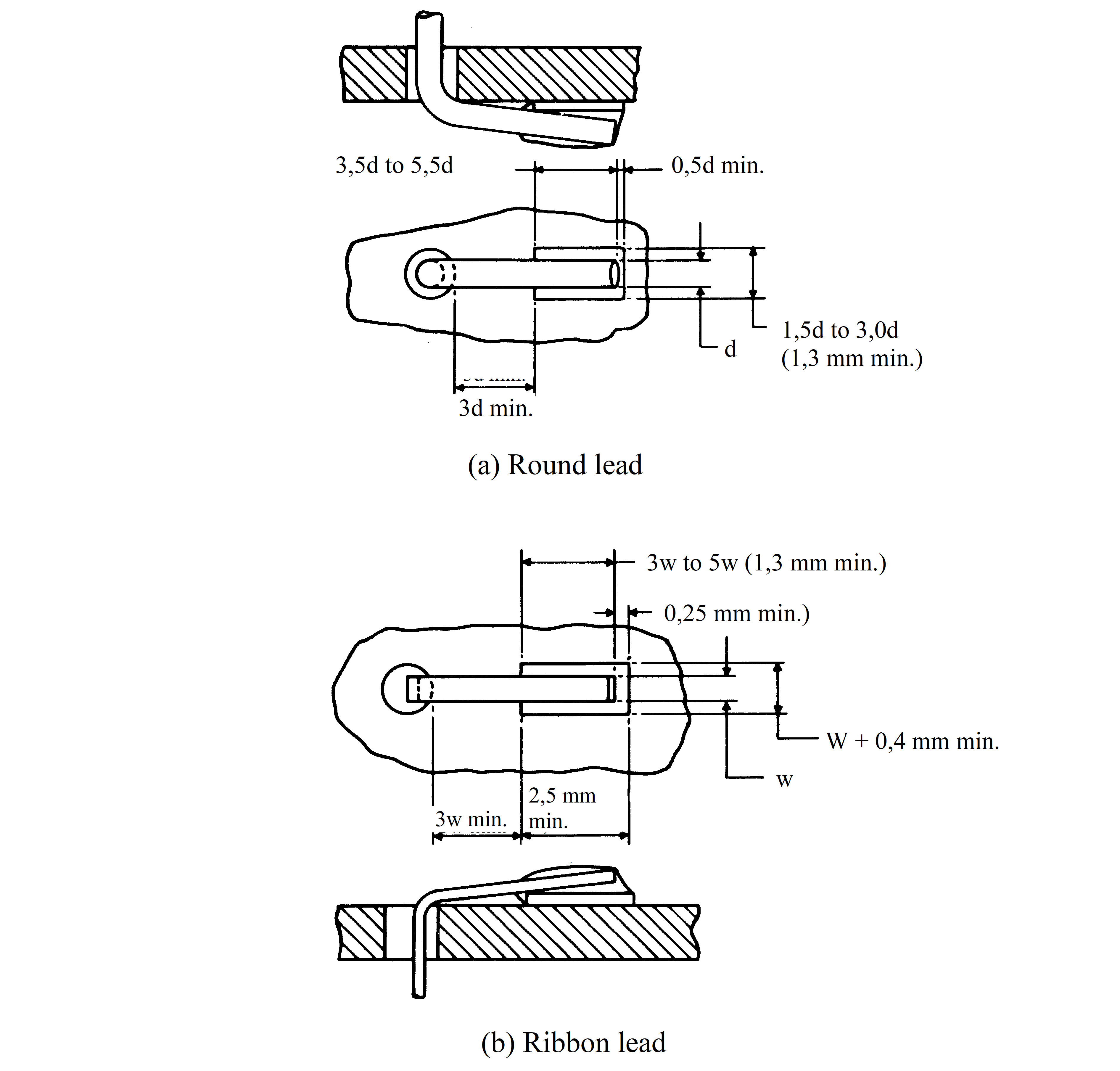 Figure 810: Methods of through-hole lapped termination
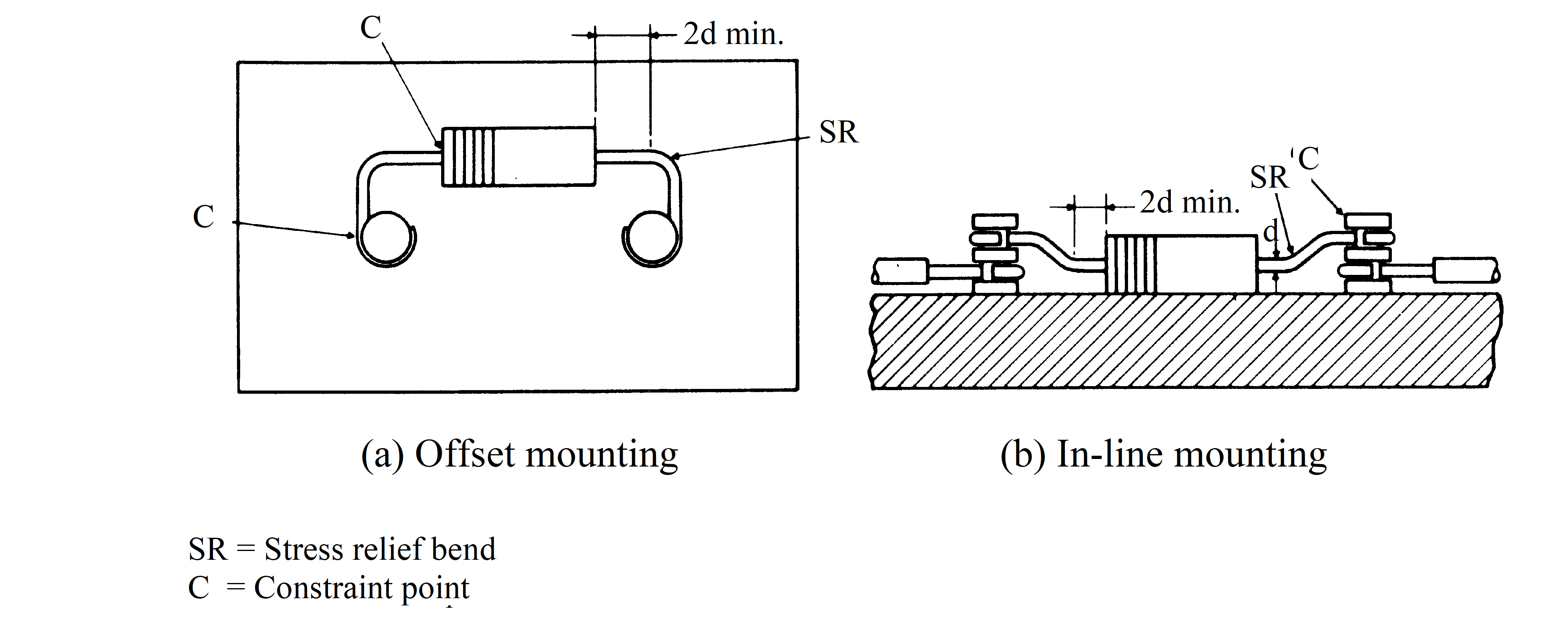 Figure 811: Method of stress relieving parts attached to terminals
Mounting of connectors to PCBs
Connectors shall be mounted in accordance with clause 8.1.
PCB connectors shall be supplied with either:
- pre-formed leads supporting stress relief bends, or
- straight, epoxy-bonded leads.
De-golding and pre-tinning of leads, in accordance with clause 7.2.3 and clause 7.2.6, shall be performed before mechanical fixing of connectors to the PCB.
Before soldering, the operator shall ensure that there is no contact between the solder fillet to be formed and the gold plating.
Connector leads shall protrude through the board in accordance with clause 8.4.3.
Attachment of conductors to terminals, solder cups and cables
General
Conductors
A conductor shall be wrapped on to a terminal in the same sense as the final curvature of the wire.
Terminals
Gold-plated terminals and solder cups shall have the gold removed in the conductor attachment area and be pretinned in accordance with clause 7.2.3.
Terminals shall be selected to fit the conductors.
Wire termination
Breakouts from cables
The length of individual wires routed from a common cable to equally-spaced terminals shall be uniform (including wire ends and stress-relief bends).
Uniform lengths prevent stress concentration in any one wire.
Insulation clearance
Where characteristic impedance or circuit parameters are not affected, the insulation clearance values stated in clause 7.2.1.4 shall apply.
Where characteristic impedance or circuit parameters are affected the insulation clearance requirements may be modified and the modification shall be documented in the process procedures.
Example: High-voltage circuits or RF coaxial line terminations.
Solid hook-up wire
Solid hook-up wire shall be supported at intervals not exceeding 30 mm.
Support shall be provided by staking or conformal coating.
Stress relief
Conductors terminating at solder connections shall incorporate stress relief.
Wicking shall be controlled.
Anti-wicking tools can be used for pre-tinning the stranded wires.
Turret and straight-pin terminals
Side route
Side route connections shall be made as shown in Figure 91 (a).
Conductors shall be wrapped around the post (see Figure 91 (c)):
- a minimum of 1/2 turn.
- a maximum of 3/4 turn.
For turret terminals, all conductors shall be confined to the guide slots.
Conductors shall not project beyond the base of the terminal.
Wires shall not be wrapped over other wires.
More than one wire may be installed in a single slot of a terminal post provided that the combined diameters of the wires are less than the width of the slot.
Wires terminating at terminals that do not have a mechanical shoulder or turret shall not be attached closer than one conductor diameter to the top of the terminal.
Bottom route
The conductor shall enter the terminal from the bottom, pass through the side slot at the top, and be wrapped as for the side route, see Figure 91 (b).
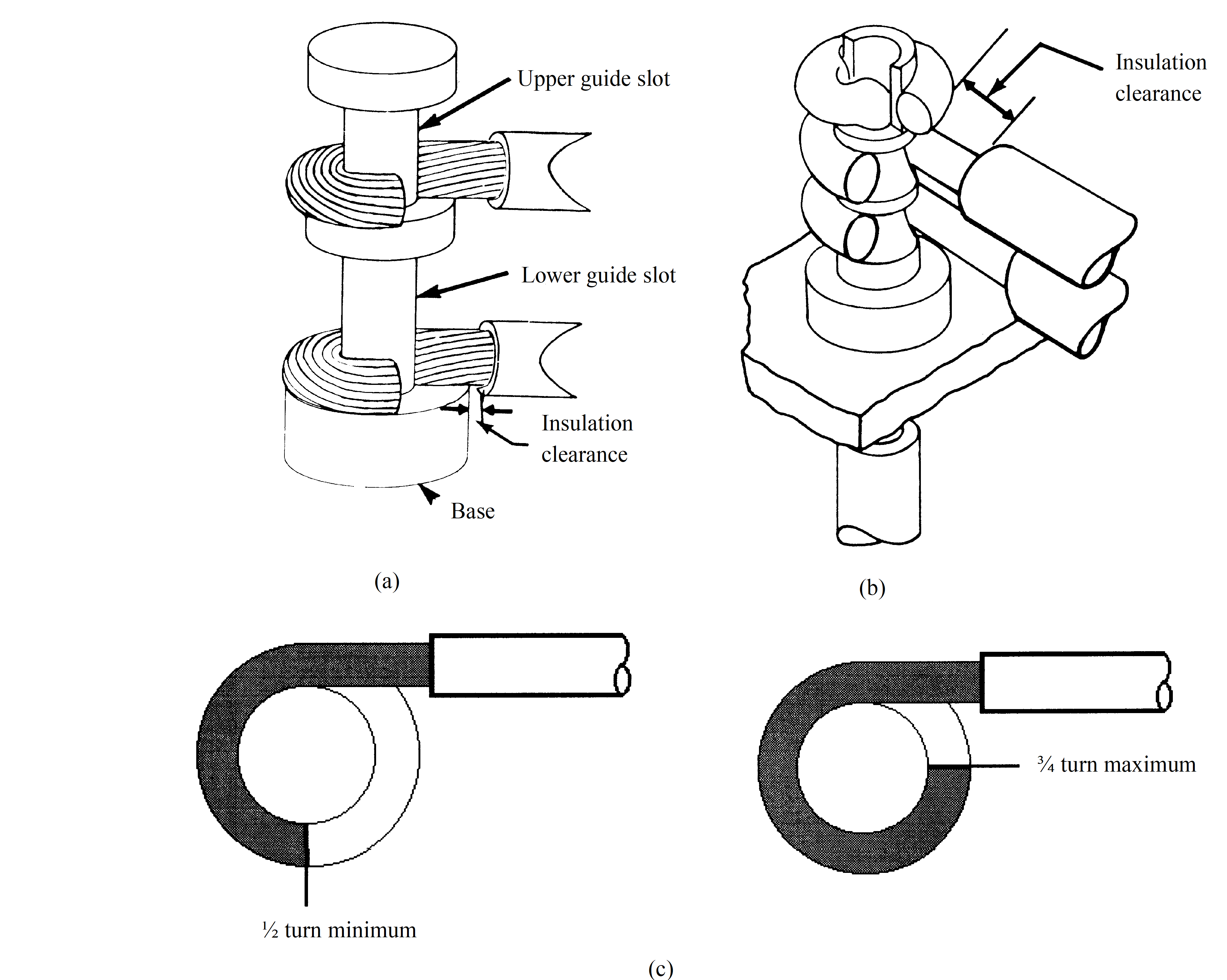 Figure 91: Side- and bottom-route connections to turret terminals
Bifurcated terminals
General
Top, side or bottom routes, or combinations thereof, shall be used.
Top route and side route shall not be used together on the same terminal.
Bottom route
Bottom route connections shall be as shown in Figure 92.
Conductors may project beyond the diameter of the base, see Figure 92 (c), provided that clearances, environmental and electrical characteristics are not compromised.
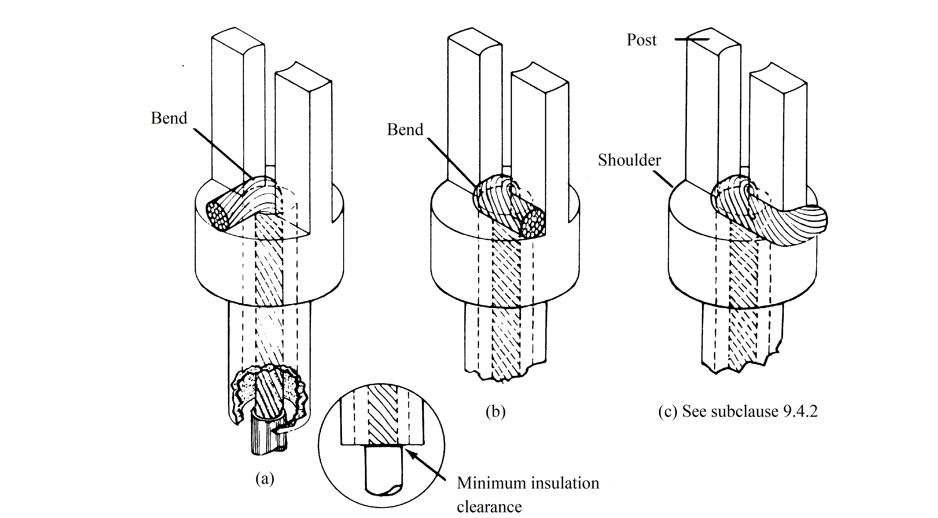 Figure 92: Bottom-route connections to bifurcated terminal
Side route
Side route connections shall be as shown in Figure 93.
The conductor shall enter the mounting slot perpendicular to the posts.
When more than one conductor is connected to a terminal, the direction of bend of each additional conductor shall alternate, see Figure 93 (b) and (d).
Side-route connections shall not project above the top of the terminal.
Conductors may project beyond the diameter of the base, see Figure 93 (c), provided that clearances, environmental and electrical characteristics are not compromised.
Conductors shall be wrapped a minimum of ¼ turn (Figure 93 (a)) to a maximum of ½ turn (Figure 93 (c)) around the post.
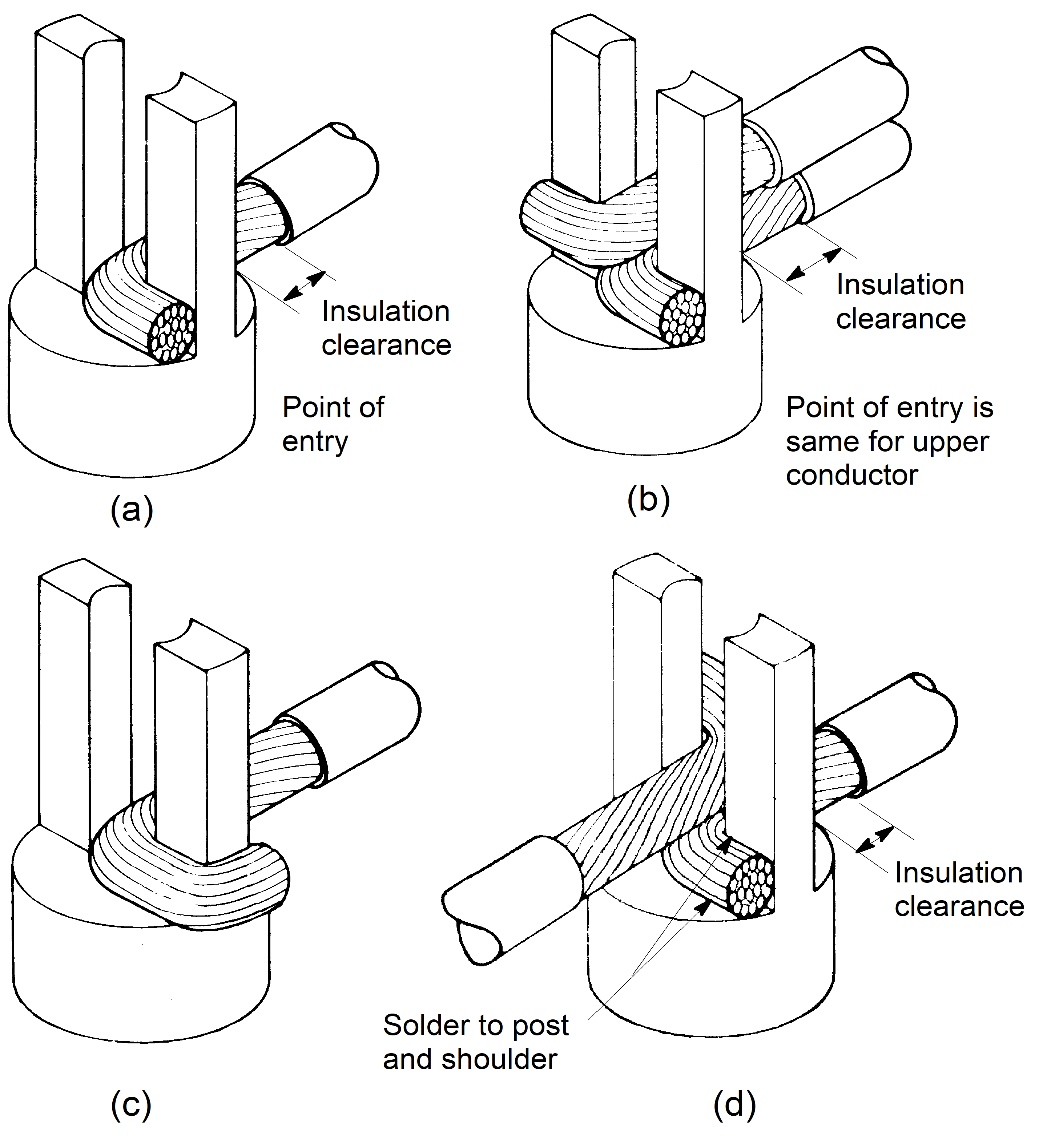 Figure 93: Side-route connection to bifurcated terminal
Top route
The top route shall not be used where side entry is possible.
Top route connections shall be as shown in Figure 94.
Conductors shall be inserted between the vertical posts to the depth of the shoulder, except for combined top and bottom routes (see clause 9.4.5).
Conductors which do not fill the gap, see Figure 94, shall be either:
- accompanied by a tinned filler wire (solid or stranded), such that the combined diameters fill the gap, or
- bent double, provided that the combined diameters fill the gap.
The top route and side route shall not be used on the same terminal.
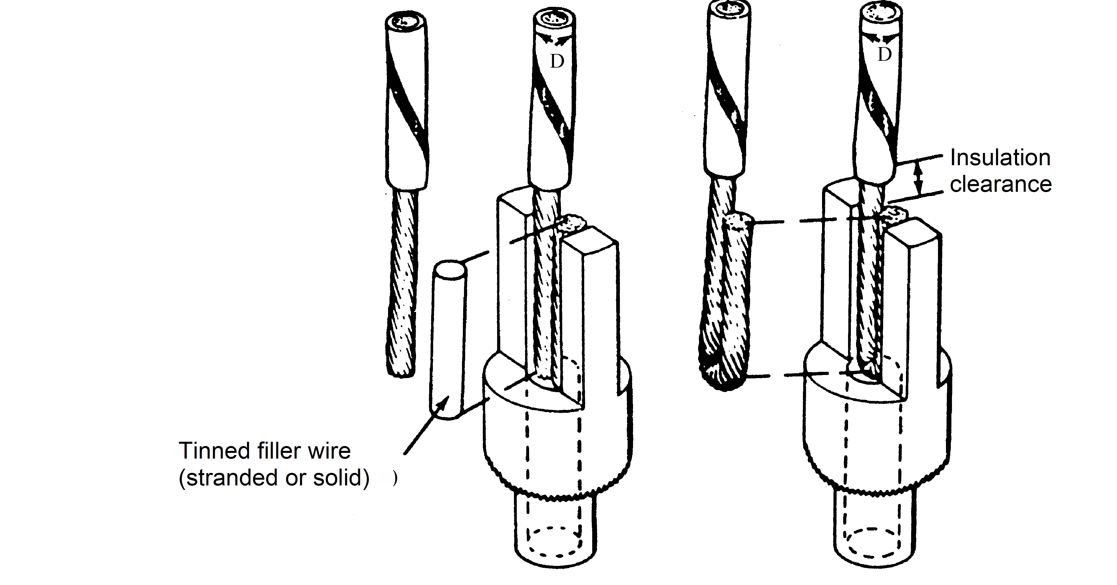 Figure 94: Top-route connection to bifurcated terminal
Combination of top and bottom routes
The bottom route conductor shall be installed before the top route conductor.
The top-route conductor shall be inserted to contact the bottom-route conductor.
Combination of side and bottom routes
The bottom route conductor shall be installed before the side route conductor.
Hook terminals
Connections to hook terminals shall be as shown in Figure 95.
The bend to attach conductors to hook terminals shall be:
- a minimum of 1/2 turn,
- a maximum of 3/4 turn.
Protrusion of conductor ends shall not damage insulation sleeving.
Where more than one conductor is attached to a terminal, the direction of bend of each conductor shall alternate (see Figure 95 (b)).
 Figure 95: Connections to hook terminals
Pierced terminals
Connections to pierced terminals shall be as shown in Figure 96.
The bend to attach conductors to pierced terminals shall be:
- a minimum of 1/4 turn,
- a maximum of 3/4 turn.
Protrusion of conductor ends shall not damage insulation sleeving.
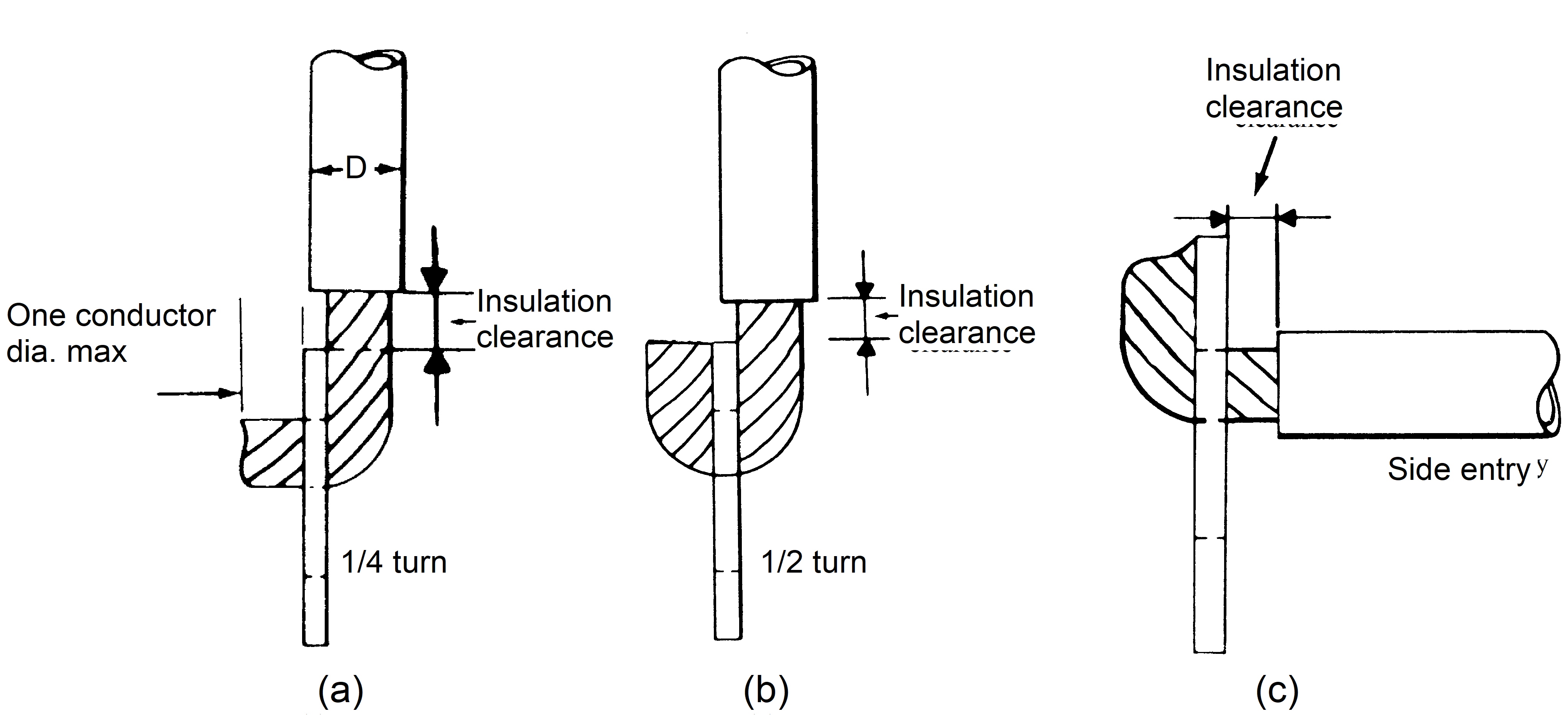 Figure 96: Connections to pierced terminals
Solder cups (connector type)
Conductors shall enter the solder cup as shown in Figure 97.
Conductors shall be bottomed in the cup.
Conductors shall be in contact with the inner wall of the cup.
Multiple conductors may be inserted provided that each is in contact with the full height of the inner wall of the cup.
Flux shall not be trapped within the solder cup.
Conductors shall not misalign floating contacts.
Example: Solid, rigid conductor wire into connectors.
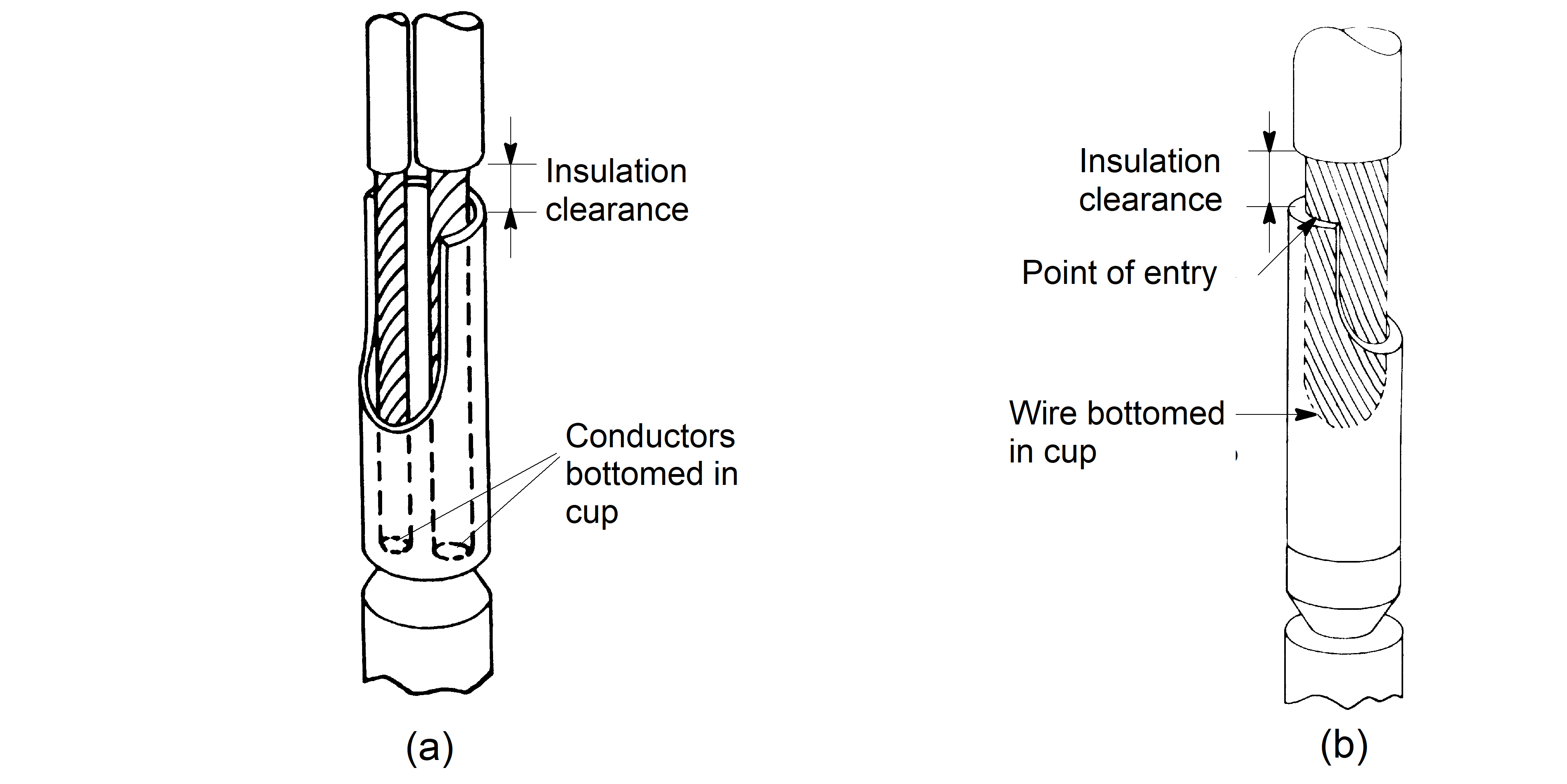 Figure 97: Connections to solder cups (connector type)
Insulation sleeving
Connections that are not protected by insulation grommets, potting, or conformal coating shall be protected by insulating sleeving.
Example: Hook terminals, solder cups and bus wires.
Insulation sleeving shall be transparent and heat-shrinkable.
A component shall not move within the sleeving when the sleeving is mechanically supported.
Heat shrinking of the sleeve shall not damage the assembly.
Wire and cable interconnections
General
Interconnection methods shall not use fluxed solder preforms within heat-shrinkable sleeves.
Soldered wire interconnection methods shall enable the removal of flux and flux residue.
Soldered wire interconnection methods shall enable visual inspection of the interconnection and surrounding materials.
After soldering, conductors shall be covered with heat-shrinkable sleeving.
Fluorocarbon sleeves shall not be used.
Fluorocarbon sleeves have high shrinkage temperatures that can damage or reflow soldered connections.
Preparation of wires
Wire insulation shall be removed using insulation strippers in accordance with clause 5.6.6.
Wire insulation clearances shall be in accordance with clause 7.2.1.4.
Pretinning shall be in accordance with clauses 7.2.5 and 7.2.6 .
Preparation of shielded wires and cables
The area of exposed shield shall be either:
- at the end of the wire or cable (end termination),or
- at any position along the length of a wire or cable (centre splice). The insulation jacket shall be removed for:
- a minimum length of 5 mm,
- a maximum length of 12 mm. The insulation jacket shall be scored and removed using a sharp cutting tool.
Example: A scalpel.
The preparation process shall not damage the exposed shield material in accordance with clauses 7.2.1.2 and 7.2.1.3.
The shield material shall be of good solderability.
The shield material shall not be pretinned.
The shield material shall be cleaned using a solvent in accordance with clause 6.4.
Pre-assembly
Heat-shrinkable sleeving
Heat-shrinkable sleeving shall provide electrical insulation and mechanical support to the finished interconnection.
The sleeving shall be cut to a length that covers the finished soldered joint and extends over the remaining insulation of each conductor for a distance of 5 mm ±2 mm.
The cut sleeving shall be threaded over one of the wires to be joined.
Conductors
Conductors shall be secured to prevent disturbance during soldering and solidification using one, or a combination of, the following methods:
- A holding fixture that clamps the wires ensuring correct alignment.
- A strand of binding wire, wrapped a minimum of 3 turns, as shown in Figure 98 (a).
Example: Bare, tinned-copper wire.
- Rings of heat-shrinkable sleeving positioned over the ends of the wire insulations, see Figure 98 (b) and (c).
- A twist-splice around the braid, see Figure 98 (c).
The conductors to be joined shall lie parallel and in contact.
Conductors may be preformed when the cable insulation prevents a parallel lay.
Bending tools for the preforming of conductors shall be in accordance with clause 5.6.4.
Wires shall be spliced using lap joints.
For shield terminations, the conductor of the grounding wire shall be positioned on the exposed shield.
Insulation overlap shall not be greater than the diameter of the largest conductor of the interconnection.
Soldering procedures
The soldering iron shall be selected in accordance with clause 5.6.7.
The solder alloy shall be in accordance with clause 6.2.
The flux shall be in accordance with clause 6.3.
Soldering aids shall be used to restrict wicking of flux or solder under the insulation in accordance with clause 5.6.8.
After solder solidification, the contour of each wire conductor shall be visible.
After solder solidification, adjacent conductors shall be connected by concave solder fillets.
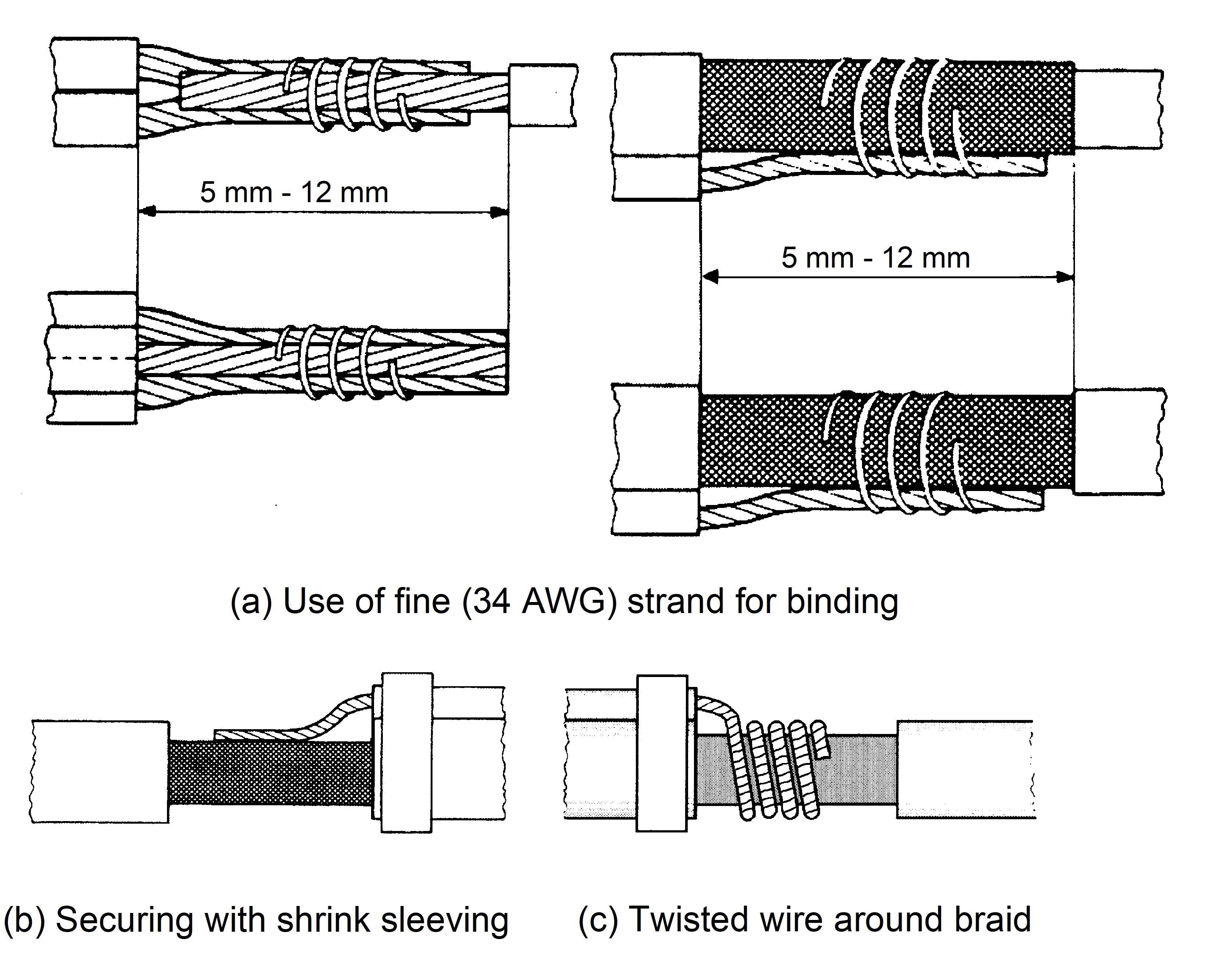 Figure 98: Methods for securing wires
Cleaning
The removal of flux and residues shall be in accordance with clause 11.
Inspection
Interconnections shall be inspected in accordance with clause 12.
Workmanship
Joints shall have a smooth, bright appearance.
The workmanship of solder joints shall be in accordance with clause 15.
The configurations in clause 15 can be applied to similar interconnections.
Sleeving of interconnections
The heat-shrinkable insulation sleeving (see clause 9.9.4.1) shall be centred over the cleaned and inspected interconnection.
The sleeving shall be shrunk using heated gas or radiant energy.
Heat shall not be applied for more than 8 seconds.
The heat-shrinking temperature shall not be exceed 140 C.
Connection of stranded wires to PCBs
Stranded wires shall be soldered to PCB terminations using lap joints or plated-through holes in accordance with Figure 99 (a), (b) and (c).
The dimensions shown in Figure 99 shall be in accordance with Table 91.
Stress relief shall be provided.
For PTFE-insulated wire, the minimum distance between the insulation and the solder fillet shall be 1 mm.
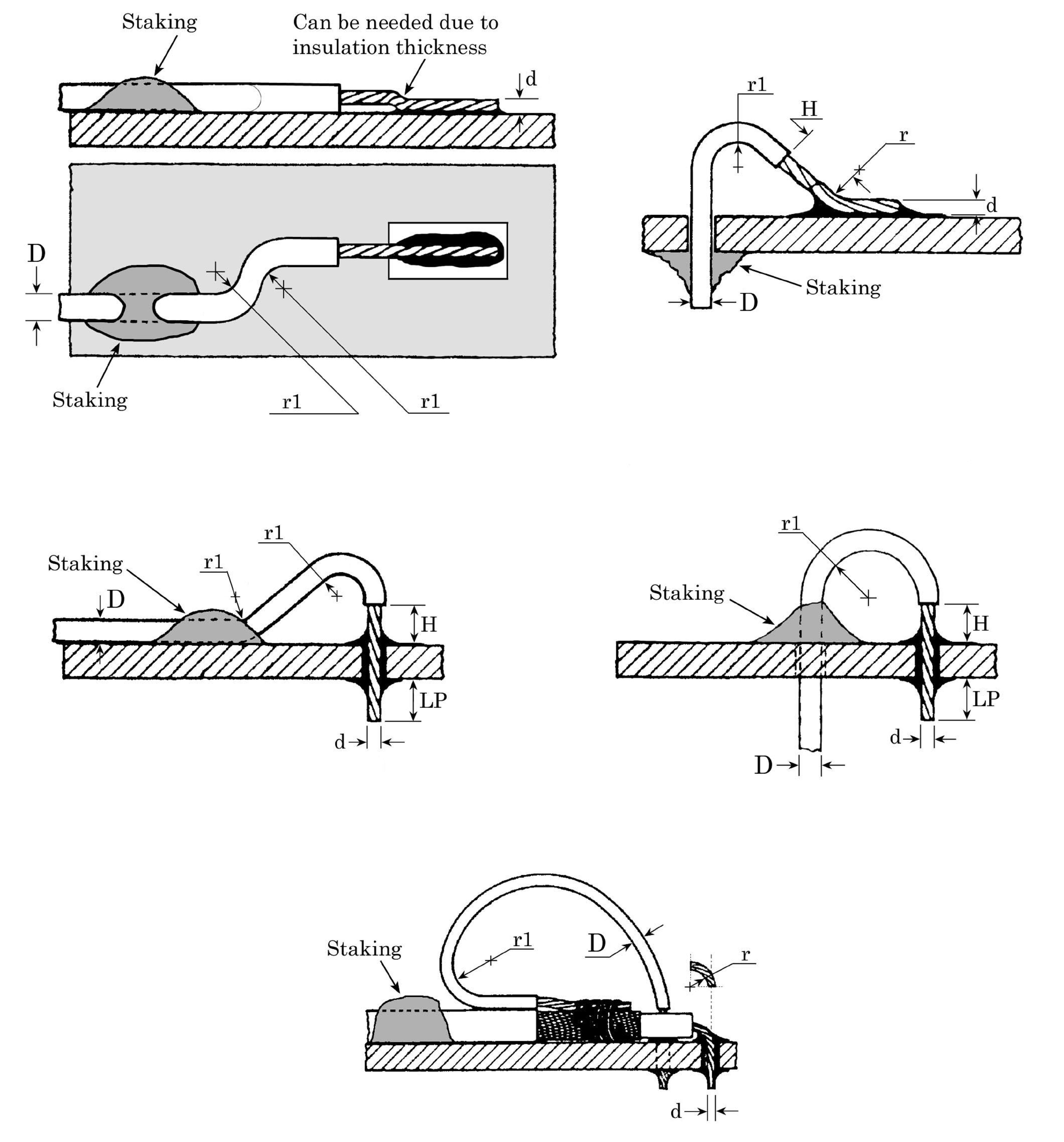 Figure 99: Connection of stranded wires to PCBs
Table 91: Dimensions for Figure 99
|
r 2 d
|
d = conductor diameter
|
|
r1 2 D
|
D = outer wire diameter
|
|
1 mm H 2 mm
|
H = insulation clearance
|
|
1,5 mm ± 0,8 mm
|
LP = lead protrusion through board
|
Soldering to terminals and PCBs
General
Securing conductors
There shall be no relative motion between conductors and terminals during soldering or solder solidification.
Conductors shall not be temporarily constrained against spring-back force during solder solidification.
Residual stresses are produced in the lead material or solder joint.
Thermal shunts
Thermal shunts shall be used to protect thermally-sensitive components.
Example: Conductors, insulation, components and previously soldered connections.
High-voltage connections
Soldered joints for corona suppression shall be performed in two stages with an intermediate inspection:
- The first soldering stage produces a standard soldered connection in accordance with clause 12;
- This connection is inspected for compliance with clause 12.2 and 12.3;
- The joint then has additional solder alloy added;
- The second soldering stage produces a final joint, see Figure 101, having:
- smooth convex fillets,
- no discontinuities,
- no severe changes in contour,
- no sharp edges or points.
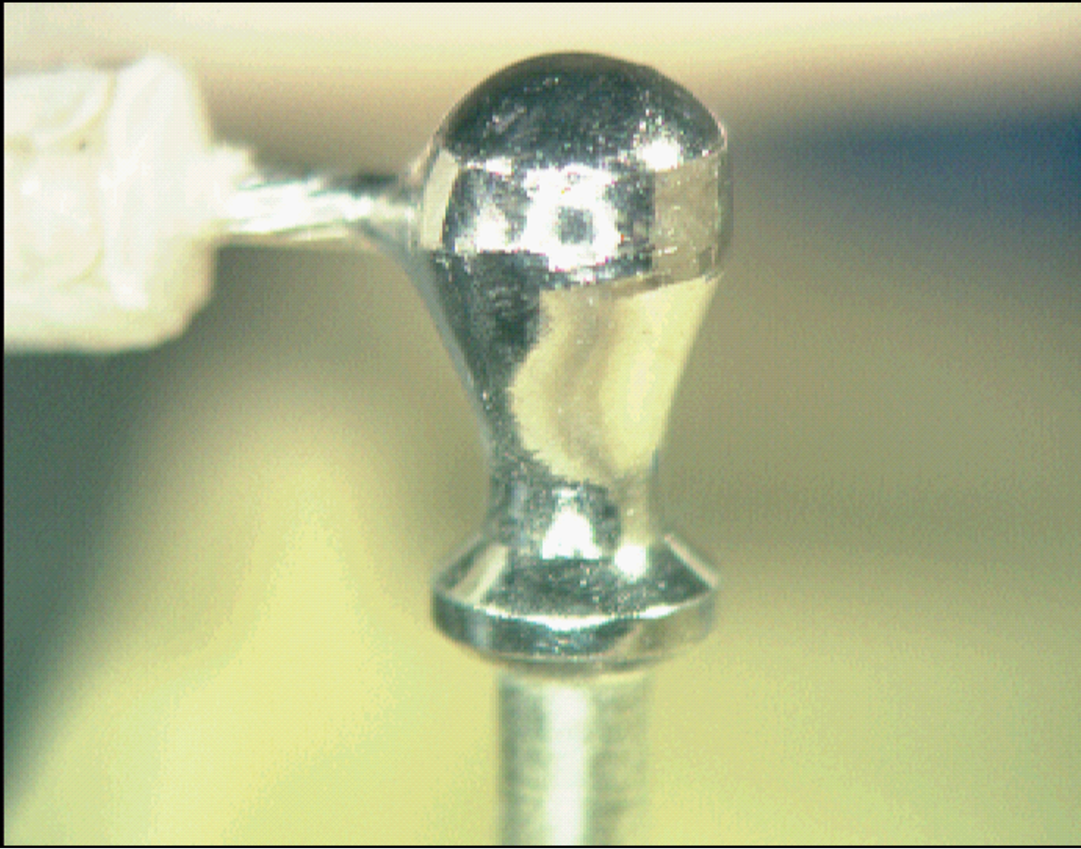 Figure 101: High voltage connection
Solder application to terminals
Soldering of swaged terminals onto PCBs
Terminals swaged to a solid flat conductor shall be soldered to one surface of the conductor.
Soldering of conductors onto terminals (except cup terminals)
A concave fillet of solder shall be present between the terminal and the sides of the conductor.
The contour of the conductor shall be visible after soldering.
Terminals with more than one wire shall have each wire in contact with, and soldered to, the terminal.
Soldering of conductors onto cup terminals
The workmanship shall be in accordance with clause 15.7.
The solder shall form a fillet between the conductor and the cup entry slot.
The fillet shall follow the contour of the cup opening.
Solder spillage may be present on the outside surface of the solder cup provided that it does not interfere with the function or the assembly of the connector.
Solder application to PCBs
Solder coverage
The molten solder shall flow around the conductor and over the termination area.
Except for high-voltage connections, the quantity of solder shall be in accordance with clause 15.
The solder for high-voltage connections shall be in accordance with clause 10.1.3.
Solder shall not obscure the contour of the conductor at the end of the insulation.
Solder fillets
Solder fillets shall be in accordance with clause 15.1 and 15.2.
A conductor mounted as a lap termination shall have a heel fillet where it bends away from the pad.
On lap terminations where one side of a conductor is flush with the edge of the termination pad, a fillet of solder shall be present along at least three of the four sides of the lead.
The fillet of solder along the lead shall extend up the side of the lead to a minimum distance of half the lead thickness or diameter.
Soldering of component leads to plated-through holes
Heat and solder side
The solder fillets shall be in accordance with clause 15.1 and 15.2.
Component side
On the component side, the terminal pad shall show solder flow-through and a solder fillet between the lead and the pad for a minimum of 25 % of the circumference, see Figure 102 (a).
Absence of component-side pad wetting may be acceptable when solder wetting is visible in the plated-through hole, see Figure 102 (b).
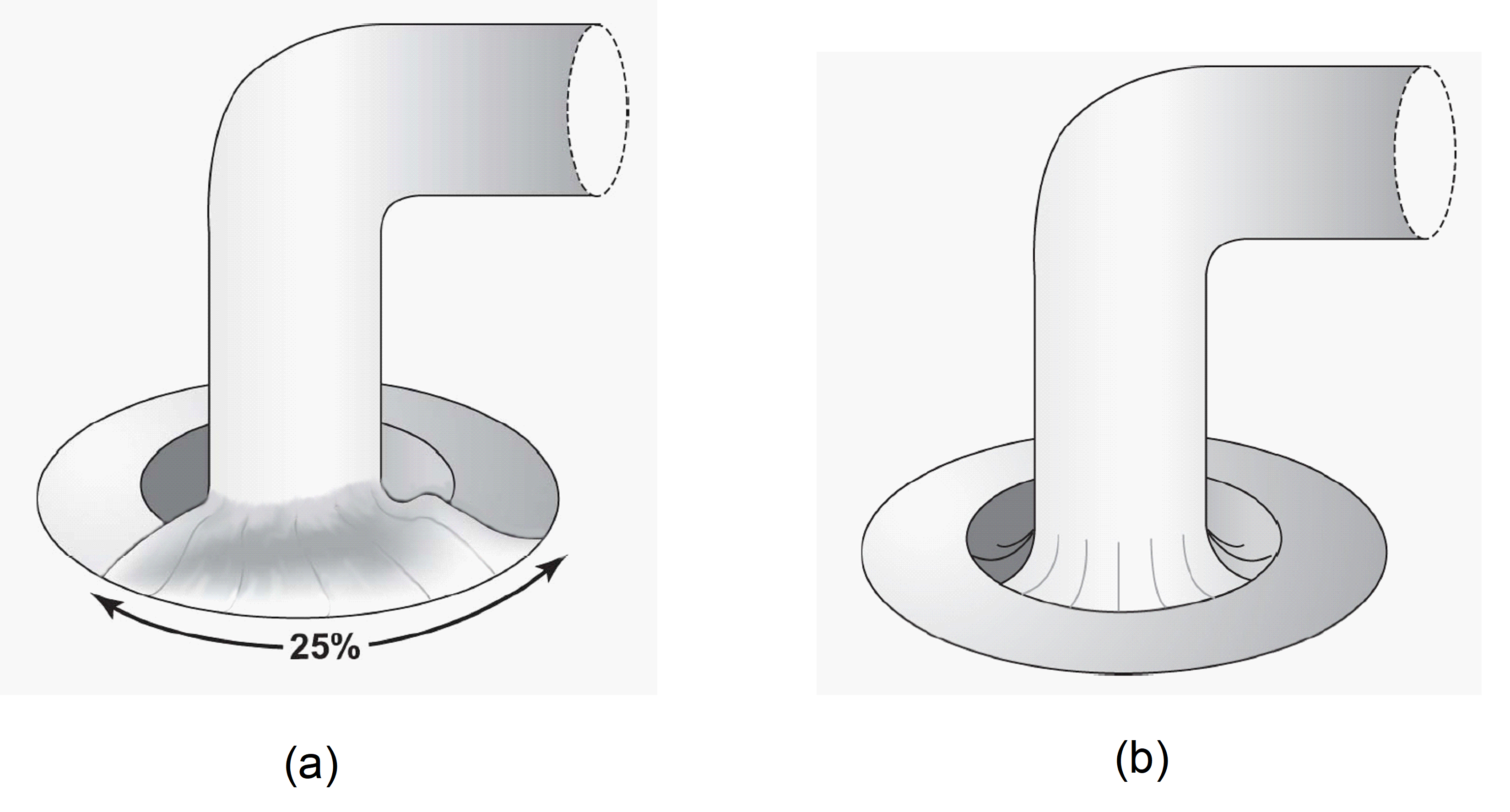 Figure 102:Minimum acceptable wetting on component side
Solder application
Solder shall be applied only to the solder side of a plated-through hole.
The soldering iron bit shall be pretinned.
The heated soldering iron bit shall be applied to the joint.
Solder shall be introduced:
- initially at the junction of the soldering iron bit and the joint.
Liquid solder between the tip and the connection promotes heat transfer.
- once heat transfer has been achieved, only to the joint. Where the rate of heat loss from the joint is too high to allow an acceptable solder joint on the component side, additional heating shall be used.
- 1 Example: High thermal masses or adjacent heat sinks.
- 2 Heat can be applied to both sides of the plated-through hole simultaneously.
Additional heating shall not damage components or materials.
The process of additional heating shall be documented.
Wicking
Soldering aids shall be used to restrict the wicking of flux or solder under insulation in accordance with clause 5.6.8.4.
Solder rework
Rework of soldered PCB assemblies shall be done when the solder joint does not meet the acceptance criteria of clause 12.
A joint shall not be reworked more than three times.
For reworking, the solder can be completely removed from the termination.
Tools and aids shall be in accordance with ECSS-Q-ST-70-28.
Repair and modification
Any repairs or modifications shall be in accordance with ECSS-Q-ST-70-28.
Cleaning of PCB assemblies
General
When the solder has solidified and cooled, flux and residue shall be removed from soldered connections using a solvent in accordance with clause 6.4.
Solvent shall be applied in such a manner that avoids its penetration under wire insulation and prevents its entry into the interior of parts.
Flux and residue shall be removed within a maximum period of 8 hours after soldering operations.
It is good practice to remove flux as soon as possible because even rosin fluxes are difficult to remove after longer ageing.
PCB assemblies shall not be immersed in cleaning solvents for more than 30 minutes for each cleaning operation.
Long immersion times can promote galvanic corrosion between adjacent metallic surfaces.
Ultrasonic cleaning
Ultrasonic cleaning shall not be used for PCBs populated with components.
Monitoring for cleanliness
Cleanliness testing
The effectiveness of the cleaning process employed for PCB assemblies (post-soldering) shall be tested using a sodium chloride (NaCl) equivalent ionic contamination test in accordance with clause 11.3.4.
Cleanliness testing may be omitted for solder assemblies using only pure rosin (ROL0) fluxes, see clause 6.3.1.
Testing frequency
For fluxes, other than pure rosin, cleanliness testing shall be done:
- at maximum intervals of six months;
- following a change in flux materials;
- following a change in process parameters;
- following actions affecting cleanability.
Statistical control methods can be used to control continuous solvent cleaning processes.
The supplier shall implement and maintain records of test results.
The records can aid early detection of a trend towards nonconformance.
When a test result is unacceptable, all PCB assemblies cleaned since the last successful test shall be subject to review by the Approval authority in accordance with ECSS-Q-ST-20.
Test limits
The sodium chloride (NaCl) ionic contamination equivalence value shall be less than 1,56 µg/cm2 of PCB surface area.
Test method
Sodium chloride (NaCl) equivalent ionic contamination shall be measured as follows:
- Use a solution of 75 % isopropyl alcohol and 25 % deionized water for the sodium chloride (NaCl) equivalent ionic contamination test.
- Calibrate the equipment using a sodium chloride solution of known quantity and composition.
Testing shall be performed according to the equipment manufacturer’s specification.
The cleanliness test values shall be as follows: - Starting resistivity: greater than 20 × 106 cm.
- Ending value: less than 1,56 g/cm2.
ESA STM 275 contains an evaluation of PCB cleanliness testing.
Final inspection
General
Each component mounting and soldered connection shall be visually inspected for compliance with clause 12.2 and 12.3 and the workmanship standards of clause 15.
Inspection shall be aided by magnification appropriate to the size of the connections between 4 times and 10 times.
Additional magnification shall be used to resolve suspected anomalies or defects.
Parts and conductors shall not be physically moved to aid inspection.
The substrate, component and component position, as well as fasteners and mounting hardware, shall be inspected in accordance with the requirements of clause 8, clause 9 and clause 10.
Acceptance criteria
Acceptable solder connections shall be characterised by:
- a clean, smooth satin to bright undisturbed surface,
- solder fillets between conductor and termination areas as described and illustrated in clause 15,
- for solder fillets of plated-through hole connections, the criteria in clause 10.3.3 apply,
- visible contour of wires and leads such that their presence, direction of bend and termination end can be determined,
- complete wetting as evidenced by a low contact angle between the solder and the joined surfaces,
- acceptable amount and distribution of solder in accordance with clause 15,
- absence of any of the defects mentioned in clauses 12.3,
- high-voltage connections in accordance with clause 10.1.3,
- stress relief.
Visual rejection criteria
The following are some characteristics of unsatisfactory conditions, any of which shall be cause for rejection:
- charred, burned or melted insulation of parts,
- conductor pattern separation from circuit board,
- burns on base materials,
- continuous discolouration between two conductor patterns.
For example measling, delamination, halo effect.
- excessive solder (including peaks, icicles and bridging), see clause 15,
- contaminated solder joints (including flux, lint and extraneous material),
- flux residue, solder splatter, solder balls, or other foreign matter on circuitry, beneath components or on adjacent areas,
- dewetting,
- insufficient solder, see clause 15,
- pits, holes or voids, or exposed base metal (excluding the ends of cut leads) in the soldered connection,
- granular or disturbed solder joints,
- fractured or cracked solder connection,
- cut, nicked, gouged or scraped conductors or conductor pattern,
- incorrect conductor length,
- incorrect direction of clinch or lap termination on a PCB,
- damaged conductor pattern,
- bare copper or base metal, excluding the ends of cut wire or leads or sides of tracks and soldering pads on substrate,
- soldered joints made directly to gold-plated terminals or gold-plated conductors using tin-lead solders,
- cold solder joints,
- component body embedded within solder fillet,
- open solder joints,
For example tombstoning.
- probe marks present on the metallization of chip devices caused by electrical testing after assembly,
- glass seal does not conform to MIL-STD-883 Method 2009.8,
- impaired stress relief.
Verification procedure
General
Any soldering configuration not covered by this standard shall be verification tested in accordance with this clause.
The supplier shall establish a verification programme to be approved by the Approval authority.
The supplier shall demonstrate verification for each combination of substrate class, staking compound, encapsulant and conformal coating as used on flight models.
The devices and associated materials shall be documented in the verification programme, including:
- package designation,
- solder alloy composition, adhesive, encapsulant, conformal coating, and printed circuit boards.
The verification test board shall support at least three devices for each assembly configuration.
The repairability of each configuration, shall be demonstrated not to damage the printed circuit board.
Verification testing shall comprise the following: - Vibration testing in accordance with clause 13.2.
Vibration testing can be performed before or after thermal testing.
- 200 thermal cycles in accordance with clause 13.3.
- Visual inspection in accordance with clause 12.
- Microsectioning in accordance with clause 13.4.
- No cracked solder joints or damaged parts.
Vibration
The test specimen shall be vibration tested.
The PCB design and mounting (including fittings such as stiffeners, frames or spacers) shall be representative of the flight model.
The test levels and durations shall be derived from the system requirements.
- 1 The vibration test levels for launcher hardware are more severe than those for other flight hardware.
- 2 Vibration testing methodology - From the input levels required by the projects in progress, the maximum deformation of the printed circuit board at the part level is established for each configuration (part type, location on the printed circuit board). The test specimen is representative of these configurations and covers at least the maximum deformations previously established, with a margin either minimum for a specific project or higher for generic applications. Nevertheless, in order to take into account test specimen imperfections, notching can be used to reduce non-representative mechanical overstresses. The part assembly (mounting condition) is defined in order to withstand the vibration levels estimated at the part level. The success of verification of the test specimen and the successful completion of QM qualification validate the assembly configuration and the implemented methodology.
A sine survey, as defined in Table 131, shall be performed before and after the high level vibration testing defined in Table 132, Table 133, and Table 134.
The severity of the vibration test shall not be less than that shown in Table 132, Table 133, and Table 134.
Input vibration levels shall be measured at the interface between the vibration plate and the PCB.
The response acceleration of the assembled PCB shall be monitored and recorded during testing.
Vibration testing shall be performed in the three orthogonal axes: one out-of-plane and two in-plane.
Table 131: Sine survey
|
Level and frequency
| |
|
Amplitude
|
0,5 g 0 to peak
|
|
Frequency range
|
10 Hz to 2000 Hz
|
|
Sweep rate
|
2 octaves / minute
|
|
Direction
|
X , Y Z axes
|
Table 132: Minimum severity for sine vibration testing
|
Range (Hz)
|
PSD Level
|
Sweep rate
| ||
|
Spacecraft
| ||||
|
25 to 100
|
20g
|
1
| ||
|
100 to 200
|
15g
| |||
|
Duration: 1 cycle up from 25Hz to 200Hz
| ||||
|
Launchers
| ||||
|
10 to 16
|
10 mm
|
1/3
| ||
|
Duration: 1 cycle up from 10Hz to 2000Hz
| ||||
Table 133: Minimum severity for random vibration testing for all applications except launchers
|
Perpendicular to PCB
|
Parallel to PCB
| ||
|
Range (Hz)
|
PSD Level
|
Range (Hz)
|
PSD Level
|
|
20 to 100
|
+ 6 dB/oct.
|
20 to 100
|
+ 6 dB/oct.
|
|
Global : 28,5 g r.m.s.
|
Global : 27,1 g r.m.s.
| ||
|
Duration: 5 minutes per axis
| |||
Table 134: Minimum severity for random vibration testing for launcher
|
Frequency
|
PSD
|
|
20 to 60
|
+ 3dB/oct.
|
|
Global: 20 g R.M.S.
| |
|
Duration: 5 minutes per axis
| |
Temperature cycling
The test specimen shall be temperature cycled in an air circulating or inert gas purged oven.
Before the start of the temperature cycling, the test specimen shall be baked-out to remove the internal humidity.
The bakeout temperature shall be between 60 °C and 80 °C"
The temperature cycle shall be between 55 C and +100 C
The rate of temperature change during the temperature cycle shall not exceed 10 C per minute.
The soak time at each temperature extreme shall be a minimum of 15 minutes.
The monitoring thermocouple shall be attached to the surface of the printed circuit board.
Microsection
At least one microsection shall be made on each configuration after vibration testing and temperature cycling.
The microsection shall be done on the device having the worst solder joint appearance identified during the visual inspection.
The Approval authority shall have access to the microsection.
The microsection shall be stored for a period of at least ten years.
Stored samples can assist the analysis of in-service failures.
Quality assurance
General
Quality assurance shall be in accordance with ECSS-Q-ST-20.
Clause 15 shall be integrated into the quality assurance plan and documentation.
Data
Quality records shall be retained for at least ten years, or in accordance with the project contract.
Example of quality records are travellers log, work orders.
Quality records shall be gathered in a report in conformance with the DRD in Annex A.
Nonconformance
Nonconformance in the soldering process shall be dispositioned in accordance with ECSS-Q-ST-10-09.
Calibration
Insulation strippers, soldering irons, measuring equipment and reference standards shall be calibrated.
A suspected or confirmed tool or equipment failure shall be recorded as a project nonconformance.
The records can aid early detection of a trend towards nonconformance.
Defective or out of calibration equipment or tools shall be labelled or removed from work areas.
The Approval authority shall be notified of the nonconformance.
Traceability
ECSS-Q-ST-20, clause 5.4 shall apply.
Workmanship standards
Visual standards shall be prepared.
The visual standards shall be available to each operator and inspector.
Examples are: Satisfactory work samples or visual aids which illustrate the quality characteristics of all types of soldered connection involved in the task.
The workmanship standards in clause 15 shall be included.
Inspection
During all stages of the process, the inspection points shall be implemented.
Inspection shall be in accordance with clause 12.
Operator and inspector training and certification
Trained and certified personnel shall be employed for soldering operations and inspections.
A training programme shall be developed, maintained and implemented by the supplier to provide excellence of workmanship and personnel skill in manual soldering.
The training programme shall include procedures for the training, certification, maintenance of certified status, recertification and revocation of certified status for soldering and inspection personnel.
Trained personnel performing soldering operations and inspections shall be certified.
Certification is based on objective evidence of soldering quality, resulting from test and inspection of soldered joints.
Personnel shall be retrained or re-assessed in the following circumstances:
- Repeated quality non-conformance.
- Change in soldering techniques.
- Change in soldering parameters.
- Additional process skills Records of the training, testing and certification status of soldering operators and inspection personnel shall be implemented and maintained.
The records are generally kept for a period of at least ten years.
Operators performing hand soldering and inspectors shall be trained and certified at a school authorized by the Approval authority.
Workmanship standards
Soldered clinched terminals
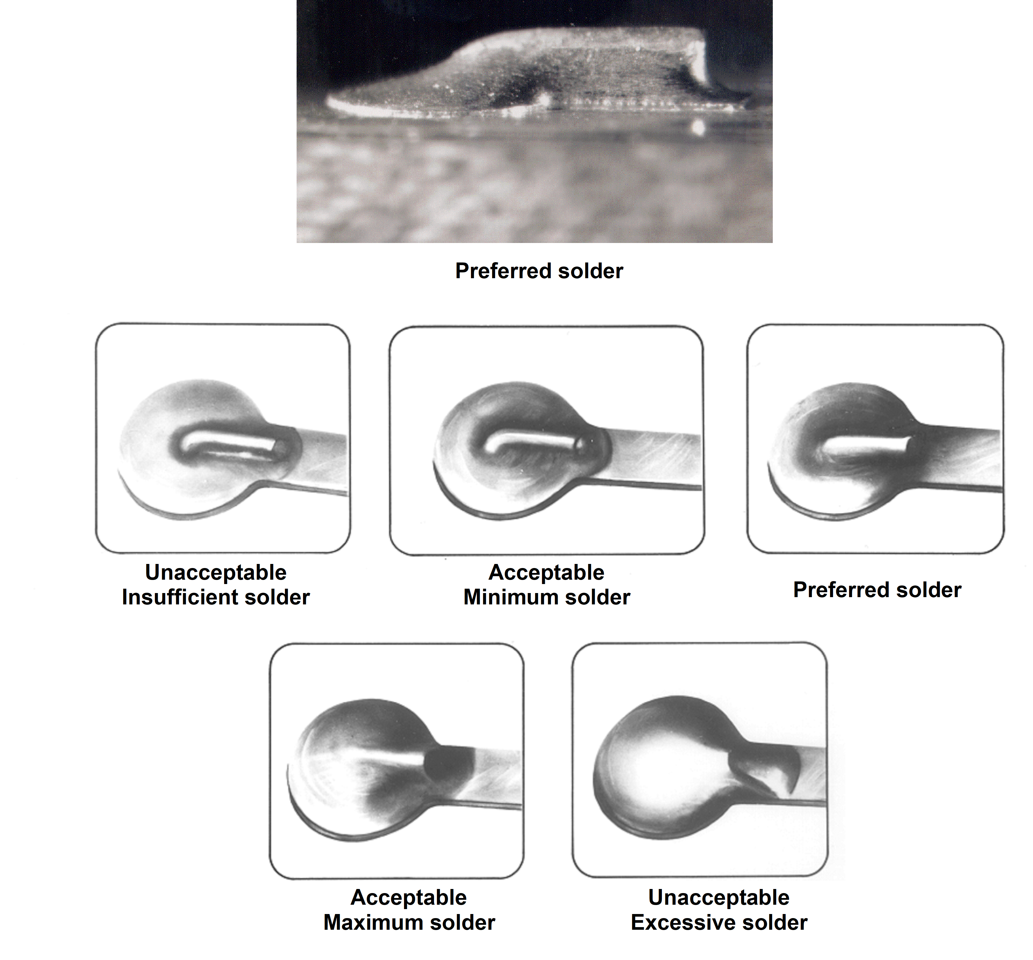 Figure 151:Soldered clinched terminals
Soldered stud terminals
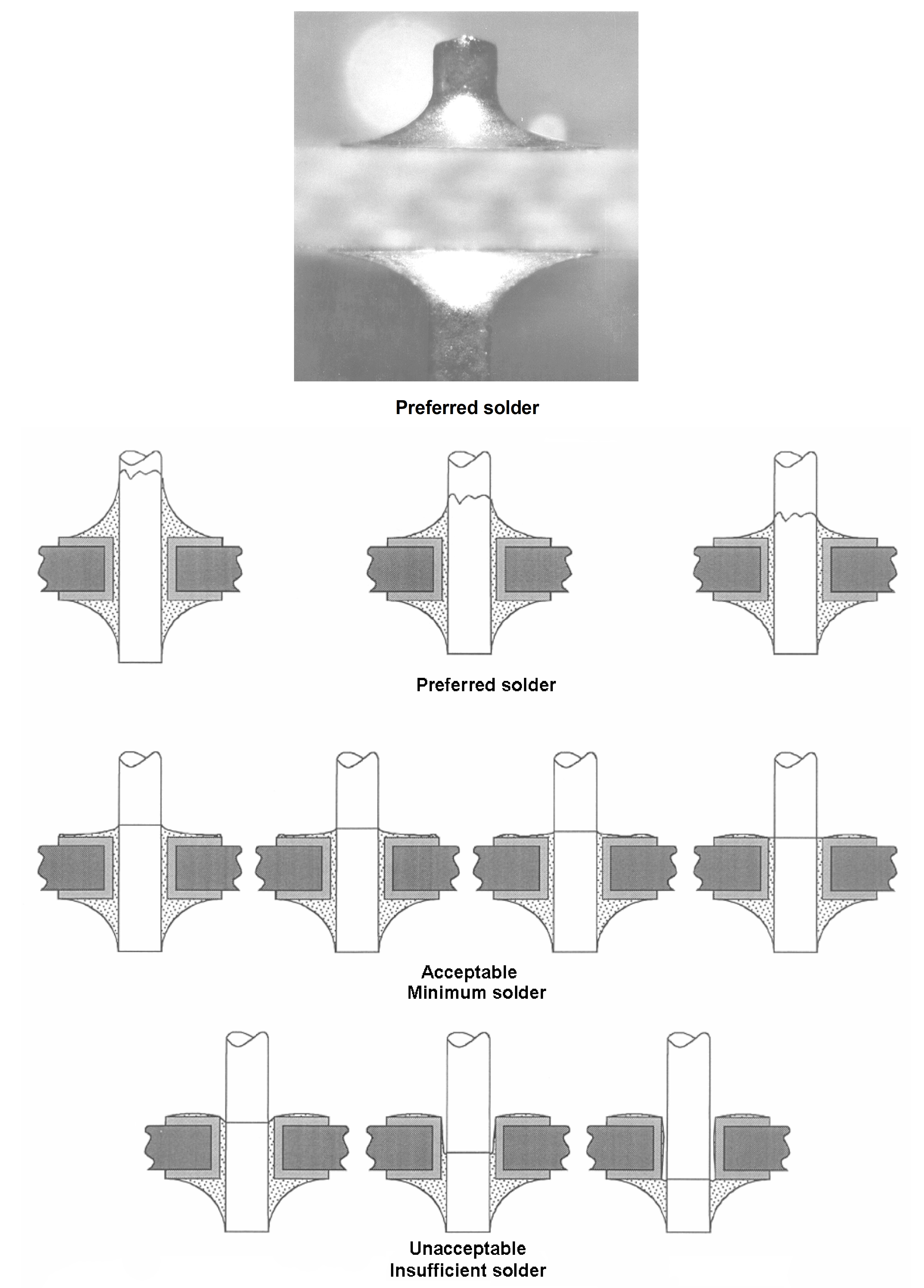 See Figure 89 and Figure 102 for other acceptable conditions.Figure 152: Soldered stud terminals
Soldered turret terminals
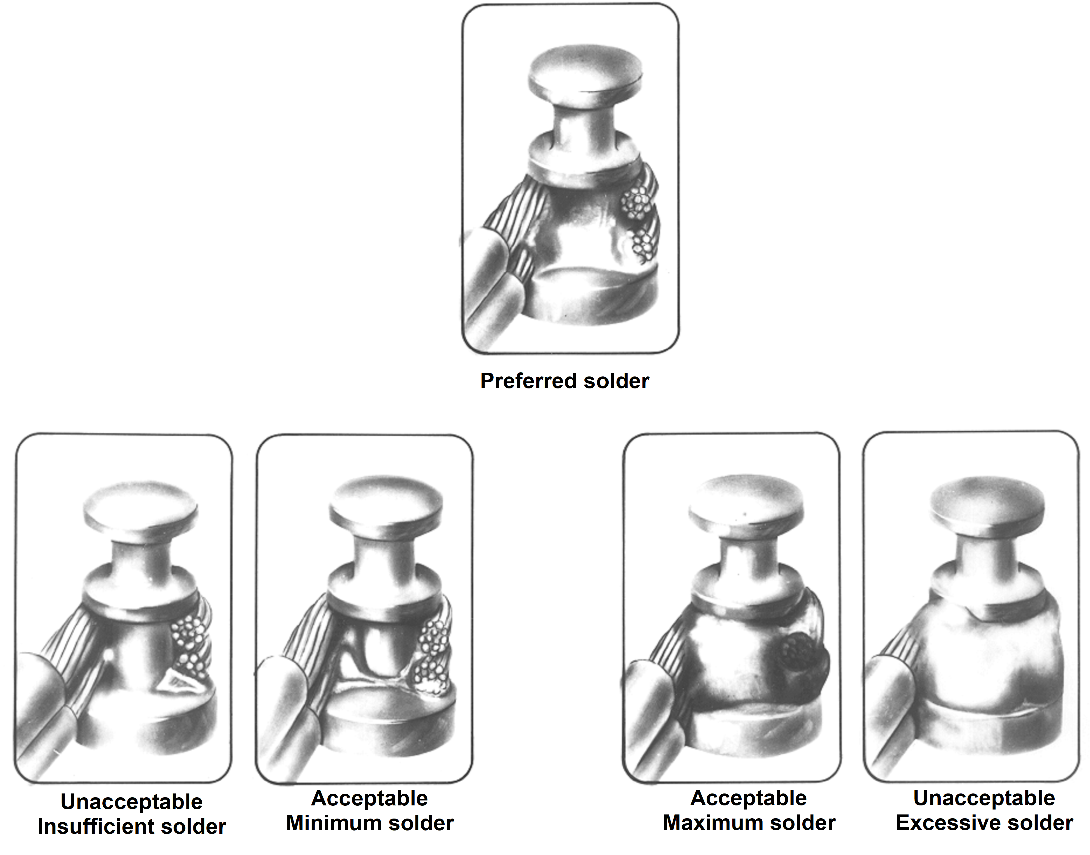 Figure 153: Soldered turret terminals with twin conductors
Solder turret terminals
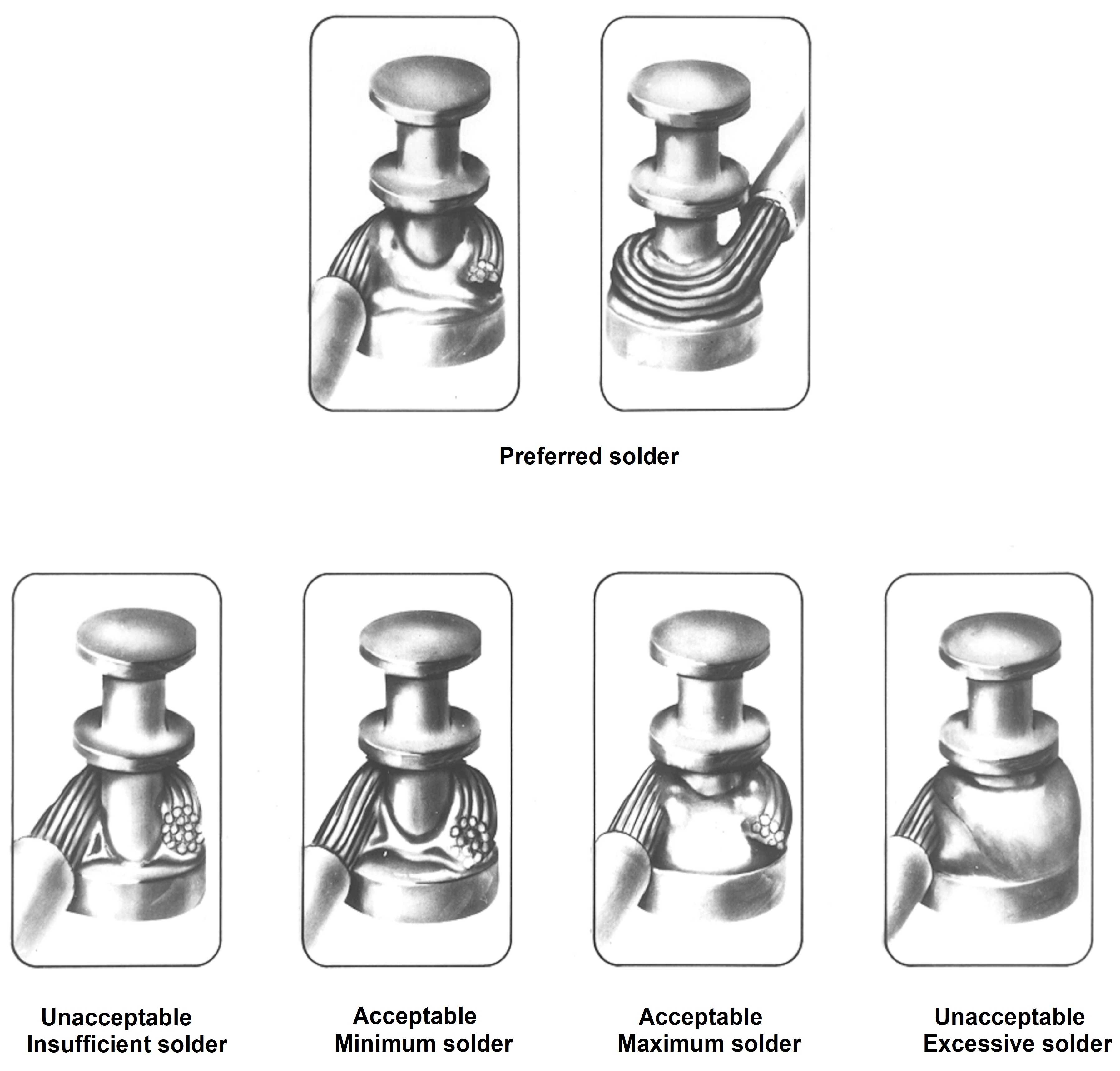 Figure 154: Soldered turret terminals with single conductors
Soldered bifurcated terminals
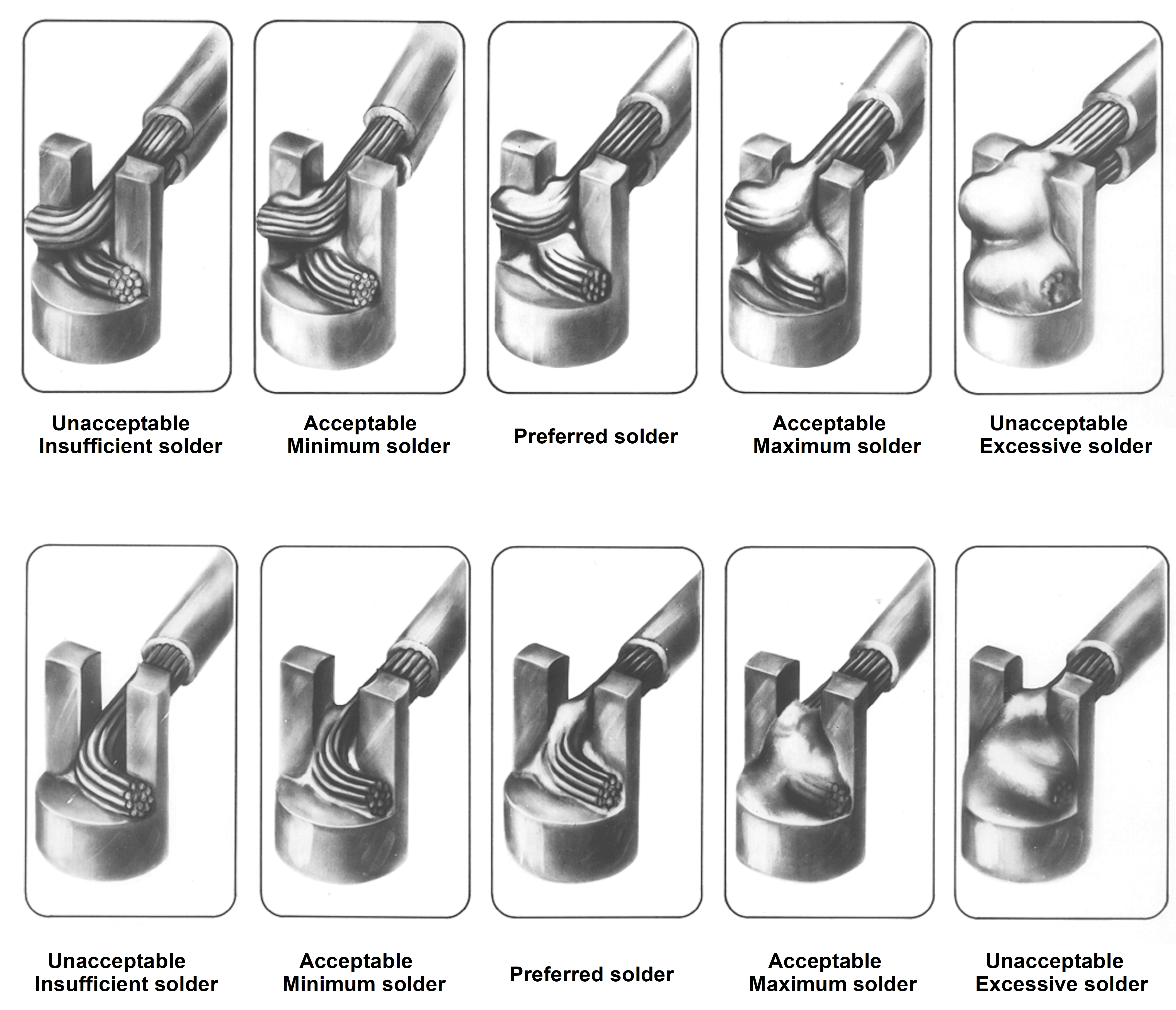 Figure 155: Soldered bifurcated terminals
Soldered hook terminals
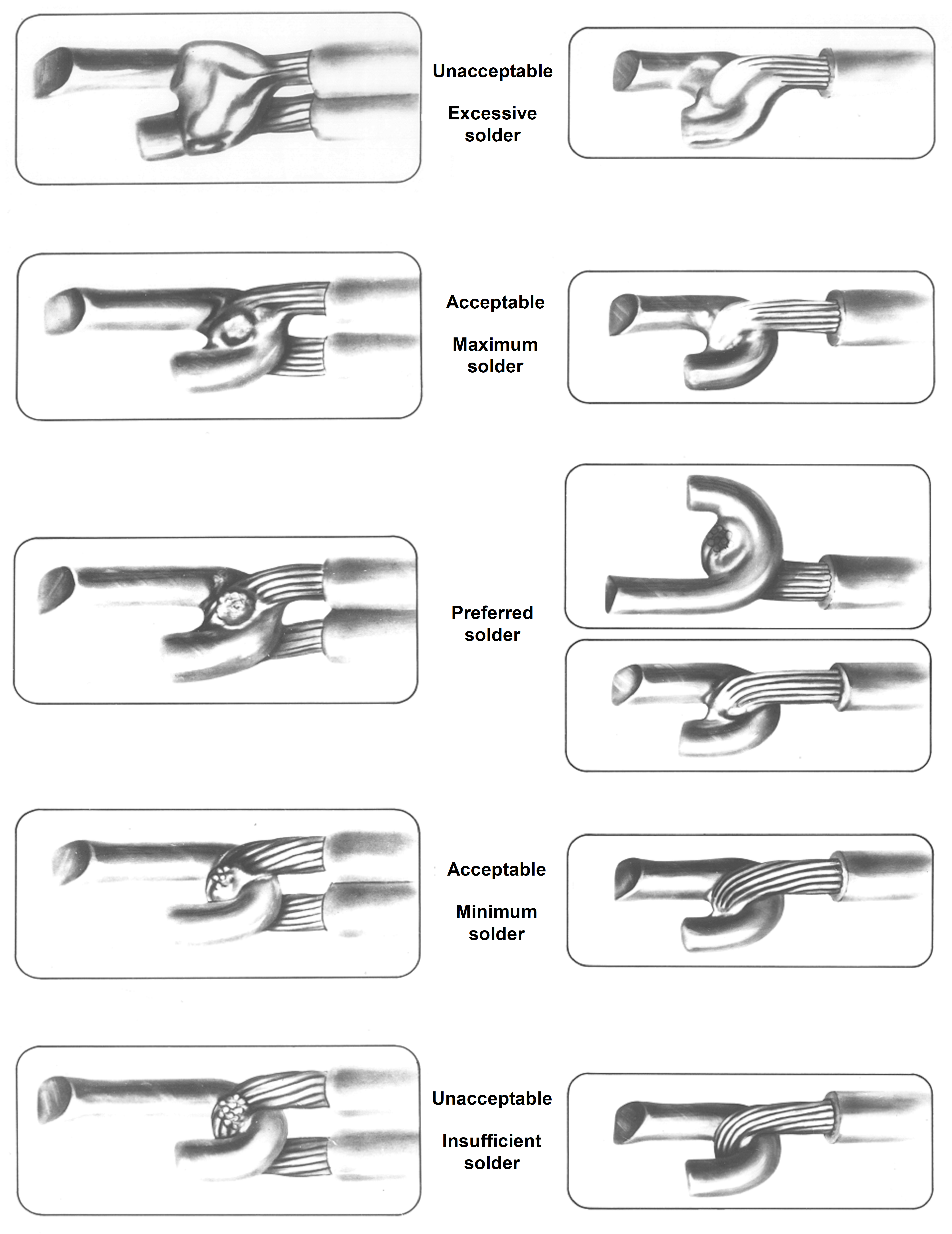 Figure 156 Soldered hook terminals
Soldered cup terminals
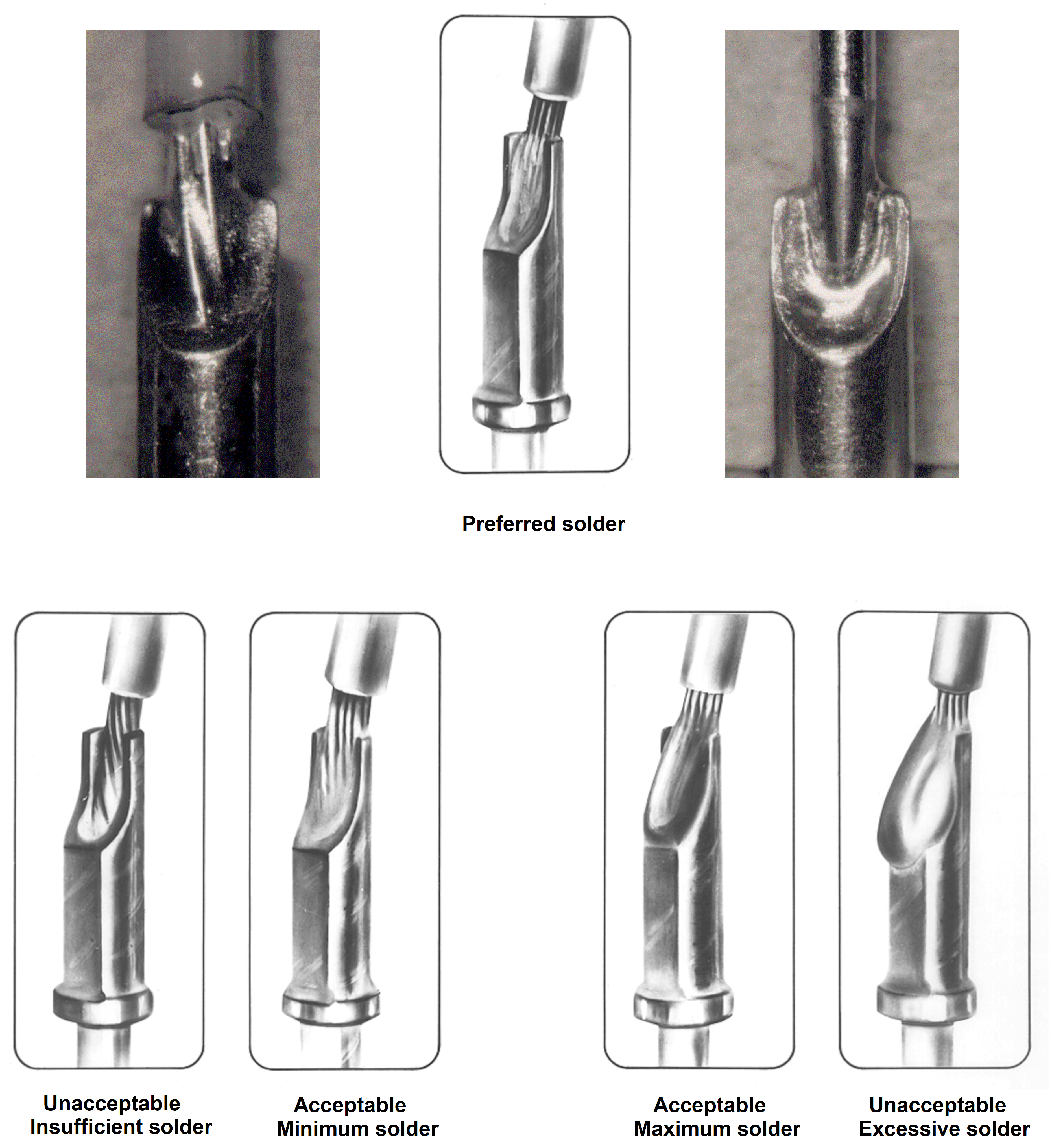 Figure 157: Soldered cup terminals
Soldered wire to shielded cable interconnections
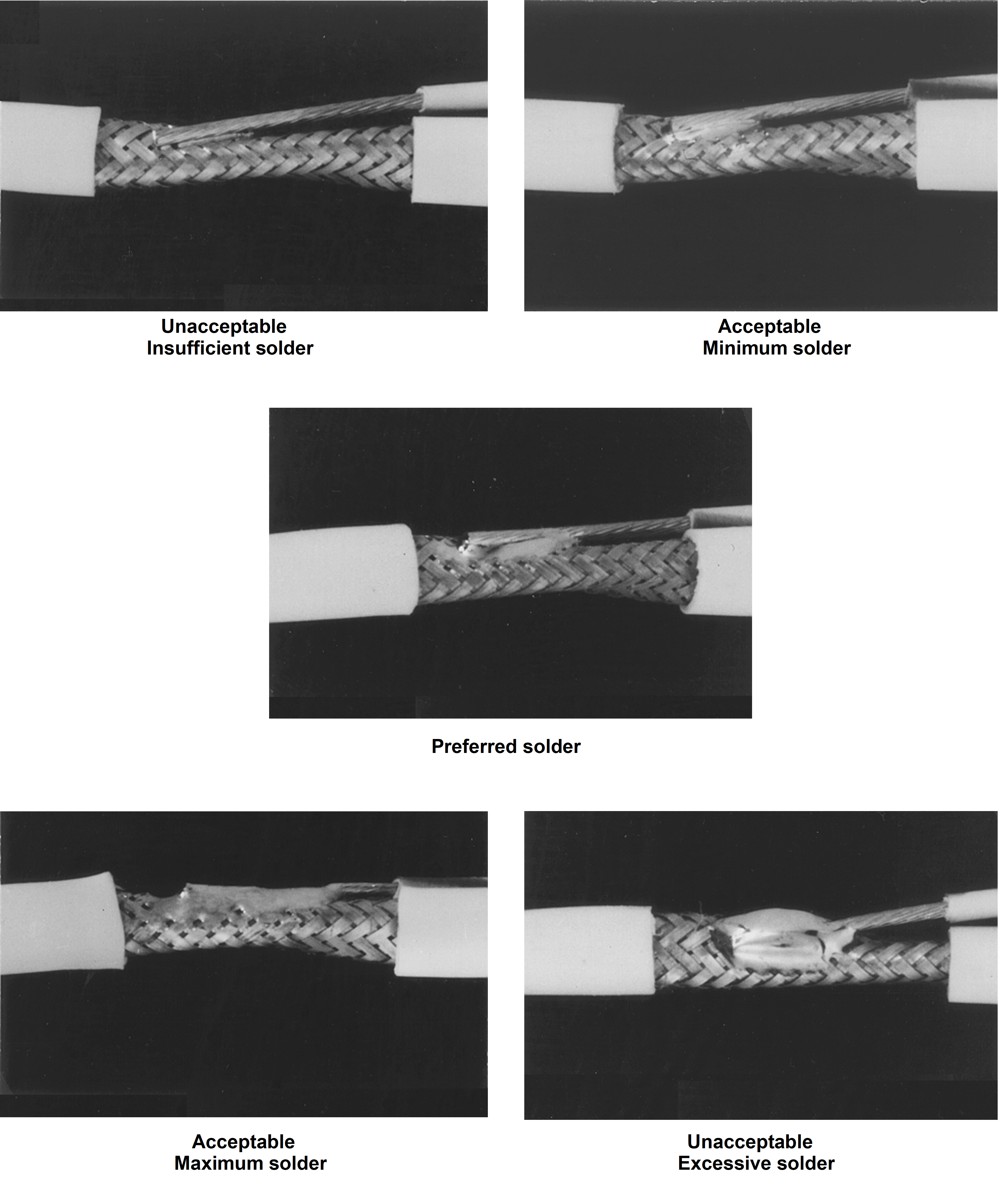 Figure 158: Handsoldered wire to shielded cable interconnections
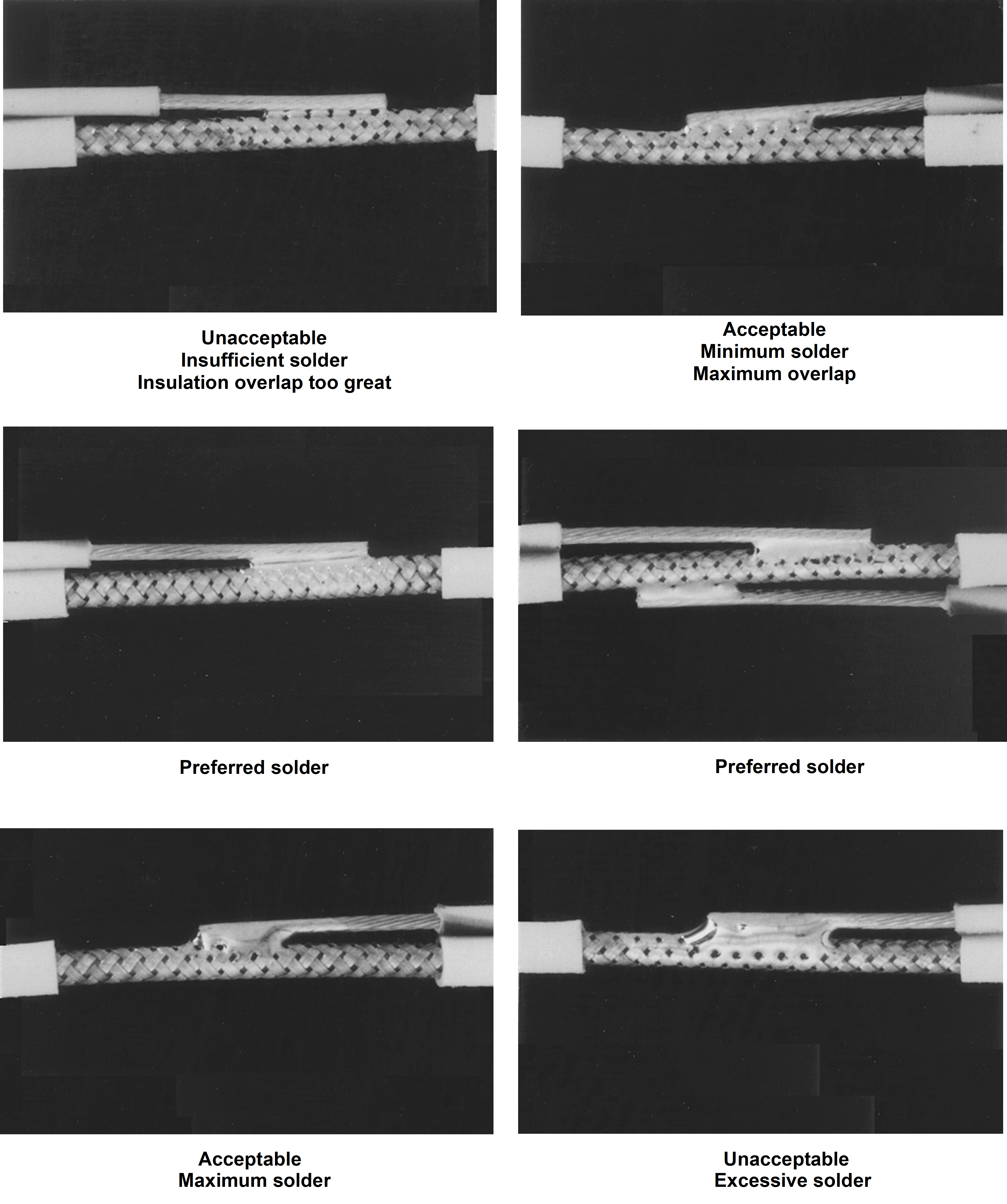 Figure 159: Handsoldered wire to shielded wire interconnections
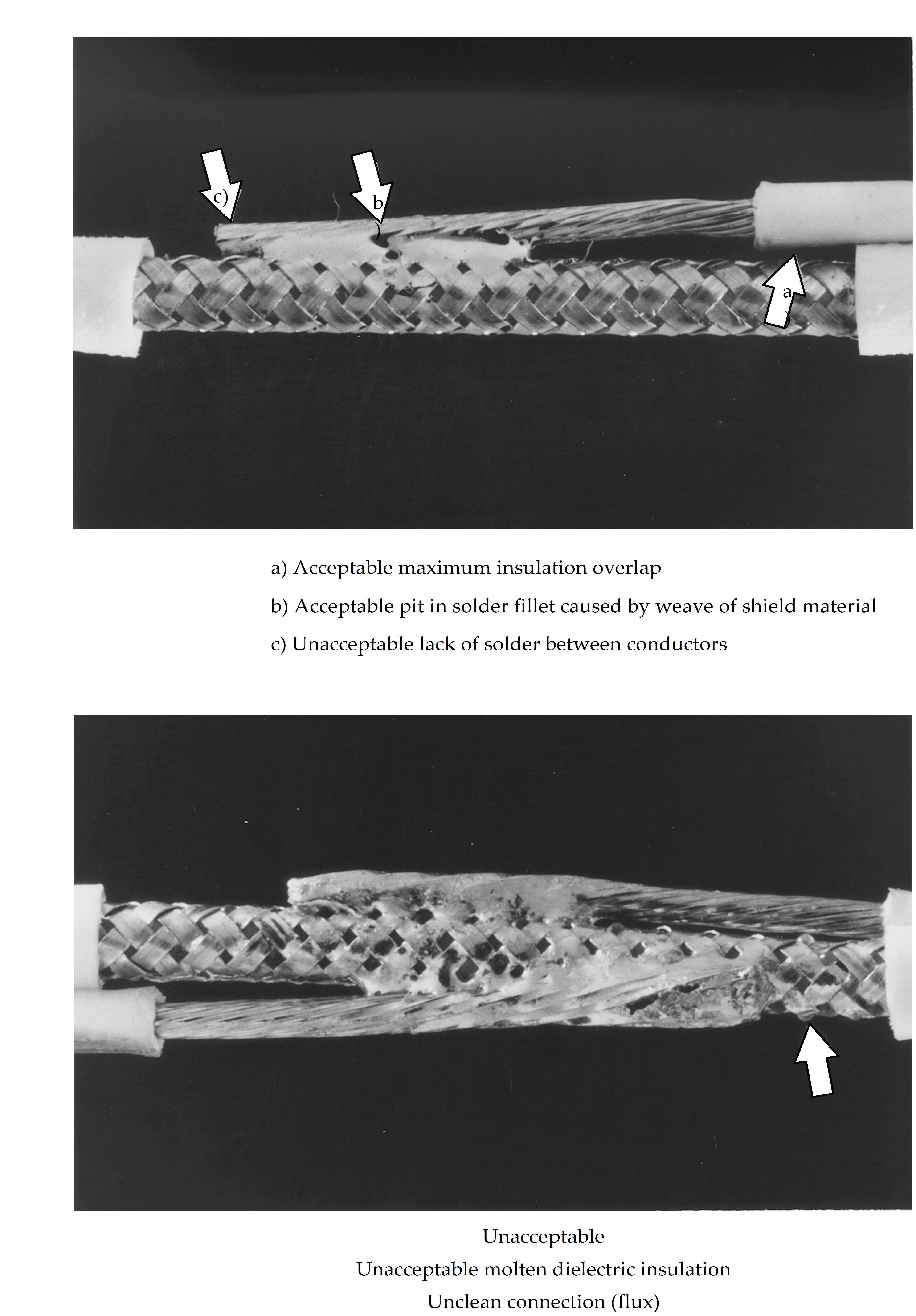 Figure 1510: Handsoldered wire interconnections - details of defects
ANNEX(normative)Report on manual soldering of high-reliability electrical connections - DRD
DRD identification
Requirement identification and source document
This DRD is called from ECSS-Q-ST-70-08, requirement 14.2b.
Purpose and objective
The purpose of this DRD is to provide in a single document all information on materials, parts, processes, testing and inspections used before and during the manual soldering of high-reliability electrical connections. This document is applicable to ensure that the assembly is made compliant to the ECSS-Q-ST-70-08.
Expected response
Scope and content
Originator
The report shall contain the name, organization and address of the originator.
System / Subsystem
The report shall identify the system/subsystem in which the assembly under inspection for compliance to manual soldering of high-reliability electrical connections is embedded.
Manufacturer
The report shall identify the manufacturer of the assembly in which manual soldering techniques for high-reliability electrical connections were used.
Assembly configuration item list
The report shall identify or refer to the assembly list detailing all the elements constituting this assembly.
Elements can be materials, processes and parts.
The report shall identify or refer to the DMPL of the assembly in which manual soldering techniques for high-reliability electrical connections were used.
The report shall identify or refer to the DML of the assembly in which manual soldering techniques for high-reliability electrical connections were used.
The report shall identify or refer to the DPL of the assembly in which manual soldering techniques for high-reliability electrical connections were used.
Engineering drawings
The report shall contain or refer to the engineering drawings of the assembly on which manual soldering of high-reliability electrical connections has been performed
Applicable documents
The report shall contain the applicable document list and the reference document list including:
- The problem report and handling of non conformance procedures to be applied.
- The list of procedures to be applied.
Procedures can be internal procedures not described in ECSS-Q-ST-70-08 describing various soldering operations.
- The list of standard to comply with.
Standards can be workmanship standards related to the acceptance and rejection criteria of soldering, international standards for ESD protection (EN 14644-1) or clean area (ISO- or ECSS Standards for the qualification and procurement of PCBs.
Evidences of compliance to manual soldering processes
The report shall demonstrate evidences that the operations and associated controls, when performing manual soldering of high-reliability electrical connections are done in compliance with ECSS-Q-ST-70-08 or other customer approved internal standards and procedures, including as a minimum:
- Records of calibration for all tools, equipment and facilities: Soldering irons,
If solder bit temperature controlled, solder bit is calibrated at incoming inspection,
Temperatures of degolding and pretinning baths.
- Statement of compliance for The controlled area with respect to cleanliness and contamination requirements,
The internal assembly procedures,
The design rules applied for the correctness of the soldering,
Operators and inspectors training and certifications,
Cleanliness of PCB assemblies,
Use of approved methods for:
The preparation of soldering,
The mounting of components,
The attachments of conductors to terminals, solder cups and cables,
Soldering to terminals and PCBs.
- Protections against ESD for: storage, assembly line, inspection line and testing areas,
Gloves, soldering aids and other used tools.
- Materials selection: Form and composition of the solder,
Characterization of fluxes,
Solvents,
Flexible insulation materials,
Chemicals composition of terminals and shapes,
Wires,
PCBs,
Components lead finishes,
Adhesives.
Verification and testing
The report shall contain all the information related to the operations and associated controls performed when verifying or testing manual soldering of high-reliability electrical connections, including as a minimum the following:
- Photographic evidences of the manual soldering to be inspected
- Visual inspection findings List of the acceptance criteria not met,
List of rejection criteria supporting the visual inspection findings.
- Discrepancies with regards to applicable standards and test specifications and procedures Cleanliness of PCB assemblies (test report),
thermal cycling (test report),
mechanical testing (vibrations test report),
electrical testing report.
- List of non conformance reports.
- Preventives and correctives actions to be managed.
Special remarks
None.
ANNEX(informative)Solder melting temperatures and choice
Table: Guide to choice of solder types
|
Solder type
|
Melting range (C)
|
Uses
| |
|
Solidus
|
Liquidus
| ||
|
63 tin solder (eutectic)
|
183
|
183
|
Soldering printed circuit boards where temperature limitations are critical and in applications with an extremely short melting range. Preferred solder for surface mount devices.
|
|
62 tin silver loaded
|
179
|
190
|
Soldering of terminations having silver and or silver palladium metallization. This solder composition decreases the scavenging of silver surfaces.
|
|
60 tin solder
|
183
|
188
|
Soldering electrical wire/cable harnesses or terminal connections and for coating or pretinning metals.
|
|
96 tin silver (eutectic)
|
221
|
221
|
Can be used for special applications, such as soldering terminal posts.
|
|
75 indium lead
|
145
|
162
|
Special solder used for low temperature soldering process when soldering gold and gold-plated finishes. Can be used for cryogenic applications.
|
|
70 indium lead
|
165
|
175
|
For use when soldering gold and gold-plated finishes when impractical to degold.
|
|
10 tin lead
|
268
|
290
|
For use in step-soldering operations, to avoid reflow of initial solder on making the second joint (limited to connections internal to devices).
|
Bibliography
|
ECSS-S-ST-00
|
ECSS system – Description, implementation and general requirements
|
|
ECSS-E-ST-10-03
|
Space engineering - Testing
|
|
ESA SP 1173
|
Evaluation of conformal coating for future spacecraft applications
|
|
ESA STM 265
|
Evaluation of thermally conductive adhesives as staking compounds during the assembly of spacecraft electronics
|
|
ESA STM 275
|
Evaluation of cleanliness test methods for spacecraft PCB assemblies
|
|
ISO 9453
|
Soft solder alloys - Chemical compositions and forms
|
|
ISO 14644-1
|
Cleanrooms and controlled environments
|
|
ISO 29454
|
Soft soldering fluxes; classification and requirements
|
|
IEC 61190-1-3 (2002)
|
Attachment materials for electronic assembly - Part 1-3: Requirements for electronic grade solder alloys and fluxed and non-fluxed solid solders for electronic soldering applications
|