
Space product assurance
Qualification of printed circuit boards
Foreword
This Standard is one of the series of ECSS Standards intended to be applied together for the management, engineering and product assurance in space projects and applications. ECSS is a cooperative effort of the European Space Agency, national space agencies and European industry associations for the purpose of developing and maintaining common standards. Requirements in this Standard are defined in terms of what shall be accomplished, rather than in terms of how to organize and perform the necessary work. This allows existing organizational structures and methods to be applied where they are effective, and for the structures and methods to evolve as necessary without rewriting the standards.
This Standard has been prepared by the ECSS Executive Secretariat, endorsed by the Document and Discipline Focal Points, and approved by the ECSS Technical Authority.
Disclaimer
ECSS does not provide any warranty whatsoever, whether expressed, implied, or statutory, including, but not limited to, any warranty of merchantability or fitness for a particular purpose or any warranty that the contents of the item are error-free. In no respect shall ECSS incur any liability for any damages, including, but not limited to, direct, indirect, special, or consequential damages arising out of, resulting from, or in any way connected to the use of this Standard, whether or not based upon warranty, business agreement, tort, or otherwise; whether or not injury was sustained by persons or property or otherwise; and whether or not loss was sustained from, or arose out of, the results of, the item, or any services that may be provided by ECSS.
Published by: ESA Requirements and Standards Division
ESTEC, P.O. Box 299,
2200 AG Noordwijk
The
Copyright: 2008 © by the European Space Agency for the members of ECSS
Change log
|
ECSS-Q-70-10A
|
First issue
|
|
ECSS-Q-70-10B
|
Never issued
|
|
ECSS-Q-ST-70-10C
|
Second issue
|
Scope
This Standard defines the requirements for evaluation, qualification and maintenance of qualification of PCB manufacturers for different types of PCBs.
This Standard is applicable to the following type of PCBs:
Rigid PCBs (singlesided, doublesided, multilayer, sequentiallaminated multilayer, metal core)
Flexible PCB (singlesided and doublesided)
Rigidflex PCBs (multilayer and sequentiallaminated multilayer)
High frequency PCBs
Special PCBs.
PCBs are used for the mounting of components in order to produce PCB assemblies performing complex electrical functions. The PCBs are subjected to thermal and mechanical shocks during their assembly such as mounting of components by soldering, rework and repair under normal terrestrial conditions, and in addition the complex PCB assembly are subjected to the environment imposed by launch and space flights.
This standard may be tailored for the specific characteristics and constraints of a space project in conformance with ECSS-S-ST-00.
Normative references
The following normative documents contain provisions which, through reference in this text, constitute provisions of this ECSS Standard. For dated references, subsequent amendments to, or revision of any of these publications do not apply. However, parties to agreements based on this ECSS Standard are encouraged to investigate the possibility of applying the more recent editions of the normative documents indicated below. For undated references, the latest edition of the publication referred to applies.
|
ECSS-S-ST-00-01
|
ECSS system — Glossary of terms
|
|
ECSS-Q-ST10-09
|
Space product assurance — Nonconformance control system
|
|
ECSS-Q-ST-20
|
Space product assurance — Quality assurance
|
|
ECSS-Q-ST-70
|
Space product assurance — Material, mechanical parts and processes
|
|
ECSS-Q-ST-70-02
|
Space product assurance — Thermal vacuum outgassing test for the screening of space materials
|
|
ECSS-Q-ST-70-08
|
Space product assurance — Manual soldering of highreliability electrical connections
|
|
ECSS-Q-ST-70-11
|
Space product assurance — Procurement of printed circuit boards
|
|
ECSS-Q-ST-70-21
|
Space product assurance — Flammability testing for the screening of space materials
|
|
ECSS-Q-ST-70-22
|
Space product assurance — Control of limited shelflife materials
|
|
ECSS-Q-ST-70-29
|
Space product assurance — Determination of offgassing products from materials and assembled articles to be used in a manned space vehicle crew compartment
|
|
IEC 60068-2-3 (1969-01)
|
Environmental testing. Part 2: Tests. Test Ca: Damp heat, steady state
|
|
IEC 60068-2-14-am 1 (1986-01)
|
Environmental testing. Part 2: Tests. Test N: Change of temperature
|
|
IEC 60068-2-20-am 2 (1987-01)
|
Environmental testing. Part 2: Tests. Test T: Soldering
|
|
IEC 60249-1-am 4 (1993-05)
|
Base materials for printed circuits. Part 1: Test methods
|
|
IEC 60326-2-am 1 (1992-06)
|
Printed boards. Part 2: Test methods
|
|
IEC 60326-5-am 1 (1989-10)
|
Printed boards. Part 5: Specification for single and double sided printed boards with platedthrough holes
|
|
IEC 60326-8 (1981-01)
|
Printed boards. Part 8: Specification for single and double sided flexible printed boards with through connections
|
|
IEC 60326-11 (1991-03)
|
Printed boards. Part 11: Specification for flexrigid multilayer printed boards with through connections
|
|
IEC 62326-4 (1996-12)
|
Printed boards. Part 4: Rigid multilayer printed boards with interlayer connections Sectional specification
|
|
IPC-4101
|
Specification for base materials for rigid and multilayer printed boards
|
|
MIL-P-50884C
|
Printed wiring, flexible and rigidflex
|
Terms, definitions and abbreviated terms
Terms from other standards
For the purpose of this Standard, the terms and definitions from ECSS-S-ST-00-01 apply.
Terms specific to the present standard
associated test coupon
small piece of PCB designated to have a limited specific set of tests performed
The associated test coupon is manufactured as part of a PCB and at the final manufacturing stage it is separated from it. The associated test coupon is thus associated with the PCB, with which it was simultaneously manufactured.
blister
delamination in the form of a localized swelling and separation between any of the layers of a lamination base material, or between base material and conductive foil or protective coating
[IEC 60194 (1999-04)]
cover layer (flexible circuit)
layer of insulating material that is applied covering totally or partially over a conductive pattern on the outer surfaces of a PCB
[IEC 60194 (1999-04)]
crazing
internal condition that occurs in reinforced base material whereby glass fibres are separated from the resin at the weave intersections
- 1 This condition manifests itself in the form of connected white spots or crosses that are below the surface of the base material. It is usually related to mechanically induced stress.
- 2 See also “measling”.
[IEC 60194 (1999-04)]
delamination
separation between plies within a base material, between base material and a conductive foil, or any other planar separation with a PCB
See also “blister”.
[IEC 60194 (1999-04)]
dewetting
condition that results when molten solder coats a surface and then recedes to leave irregularlyshaped mounds of solder that are separated by areas that are covered with a thin film of solder and with the basis metal not exposed
[IEC 60194 (1999-04)]
flexible PCB
PCB either single, double sided or multilayer consisting of a printed circuit or printed wiring using flexible base materials only
[IEC 60194 (1999-04)]
haloing
mechanicallyinduced fracturing or delamination, on or below the surface of a base material, that is usually exhibited by a light area around holes or other machined features
[IEC 60194 (1999-04)]
high frequency PCB
PCB used for high frequency applications, that has specific requirements to the dielectric properties of the base laminates as well as special dimensional requirements to the layout for electrical purposes
inclusions
foreign particles, metallic or nonmetallic, that may be entrapped in an insulating material, conductive layer, plating, base material or solder connection
[IEC 60194 (1999-04)]
key personnel
personnel with specialist knowledge responsible for defined production or product assurance areas
measling
condition that occurs in laminated base material in which internal glass fibres are separated from the resin at the weave intersection
- 1 This condition manifests itself in the form of discrete white spots or “crosses” that are below the surface of the base material. It is usually related to thermallyinduced stress.
- 2 See also “crazing”.
[IEC 60194 (1999-04)]
metal core PCB
PCB using a metal core base material
[IEC 60194 (1999-04)]
multilayer PCB
PCB that consist of rigid or flexible insulation materials and three or more alternate printed wiring and/or printed circuit layers that have been bonded together and electrically interconnected
[IEC 60194 (1999-04)]
prepreg
sheet of material that has been impregnated with a resin and cured to an intermediate stage
Bstaged resin.
[IEC 60194 (1999-04)]
printed circuit board (PCB)
printed board that provides both pointtopoint connections and printed components in a predetermined arrangement on a common base
This includes singlesided, double sided and multilayer PCBs with rigid, flexible, and rigidflex base materials.
[IEC 60194 (1999-04)]
rigid doublesided PCB
doublesided PCB, either printed circuit or printed wiring, using rigid base materials only
[IEC 60194 (1999-04)]
rigidflex PCB
PCB with both rigid and flexible base materials
[IEC 60194 (1999-04)]
rigidflex doublesided PCB
doublesided PCB, either printed circuit or printed wiring, using combinations of rigid and flexible base materials
[IEC 60194 (1999-04)]
rigidflex multilayer PCB
multilayer PCB, either printed circuit or printed wiring, using combinations of rigid multilayer and flexible single and doublesided base materials
rigid PCB
PCB using rigid base materials only
[IEC 60194 (1999-04)]
rigid singlesided PCB
singlesided PCB, either printed circuit or printed wiring, using rigid base materials only
[IEC 60194 (1999-04)]
rigid multilayer PCB
multilayer PCB, either printed circuit or printed wiring, using rigid base materials only
[IEC 60194 (1999-04)]
scratch
narrow furrow or grove in a surface
It is usually shallow and caused by the marking or rasping of the surface with a pointed or sharp object.
[IEC 60194 (1999-04)]
sequentially laminated multilayer PCB
multilayer PCB that is formed by laminating together through hole plated doublesided or multilayer PCBs
Thus, some of its conductive layers are interconnected with blind or buried vias.
[IEC 60194 (1999-04)]
test pattern
part of the PCB that refers to the copper pattern on and within the PCB substrate for a specific test
Abbreviated terms
For the purpose of this Standard, the abbreviated terms from ECSS-S-ST-00-01 and the following apply:
|
Abbreviation
|
Meaning
|
|
CAD
|
computer aided design
|
|
|
computer aided manufacturing
|
|
M
|
major nonconformance
|
|
m
|
minor nonconformance
|
|
n.a.
|
not applicable
|
|
NRB
|
nonconformance review board
|
|
PCB
|
printed circuit board
|
|
PID
|
process identification document
|
|
PTH
|
platedthrough hole
|
|
PTFE
|
polytetrafluoroethylene
|
|
r.m.s.
|
rootmeansquare
|
|
TBD
|
to be defined
|
Principles
General
This Standard details the steps to obtain from the PCB manufacturer the qualification for supplying PCBs of an identified technology.
These steps are:
Evaluation (see clause 5);
Qualification (see clause 6):
Test and inspections (see clause 7),
Qualification approval (see clause 6.6);
Maintenance of qualification (see clause 6.7).
Roles
For the need of this Standard the roles “PCB manufacturer”, “supplier”, “customer” and “qualification authority” have been explicitly introduced to allow proper allocation of requirements:
The “PCB manufacturer” is the entity that manufactures the PCB.
The “supplier” is the entity that uses the PCB for an instrument, for instance a subcontractor that delivers an electronics box. The supplier procures the PCB from the PCB manufacturer.
The “customer” is the entity that uses the supplier’s product for a project, for instance a prime contractor that integrates an electronics box into a spacecraft payload. The role of supplier can coincide with the one of customer. The term customer does not refer to being the customer of the PCB manufacturer but refers to being the (prime) contractor of a space organisation initiating a space project.
The “qualification authority” is the entity that reviews and accepts the qualification programme, evaluates the test results and grants the final approval. The role of customer can coincide with the one of qualification authority.
Specification of test requirements
Clause 7 describes the tests within the qualification programme in which the following three levels of requirement specifications are used:
The requirement specifications that are generic for all types of PCBs are listed in clause 7.
The requirement specifications that are specific to a particular type of PCB are listed in clause 9 and are referred to with the term “requirement” in clause 7.
The requirement specifications that are determined by the supplier are referred to with the term “supplier’s specification” in clause 7.
Evaluation
General
The PCB manufacturer who applies for the qualification of his PCB manufacturing line shall:
- request for an evaluation in conformance with clause 5.2;
- supply evaluation PCBs in conformance with clause 5.3;
- have a manufacturing line audit performed in conformance with clause 5.4.
If the result is satisfactory, the qualification authority can authorize the goahead of the qualification programme for each of the technologies that have been accepted.
The PCB manufacturer and the qualification authority shall agree on the evaluation tests to be performed.
The evaluation tests can be an appropriate subset of the tests performed within the qualification programme.
Request for evaluation
The PCB manufacturer’s request for evaluation shall contain:
- a description of the technology for which the PCB manufacturer wishes to be evaluated;
- a description of the manufacturing line;
- past experience.
Applications shall be signed by the person responsible for production and product assurance.
Applications shall be addressed to the qualification authority.
Evaluation PCBs
The PCB manufacturer shall produce three evaluation PCBs of each type with the materials, processes and equipment that are intended for use in subsequent production.
The evaluation PCBs shall be representative in terms of technology for which the PCB manufacturer applies for qualification.
The term technology refers, among others, to:
- Dimensions of the boards, vias, pads and tracks
- Number of layers
- Pattern design.
The evaluation PCBs shall represent the highest technological capability for which the PCB manufacturer applies for qualification.
The PCB manufacturer shall perform the evaluation test and document it in conformance with Annex A.
The evaluation PCBs can be inspected at an independent certified test house.
The evaluation PCBs shall be provided with associated test coupons.
Line audit
Provided that the evaluation PCBs are accepted, the qualification authority shall audit the manufacturing line when PCB production is in progress.
Before or during the audit, the PCB manufacturer shall make the following documents available to the customer:
- Company organigram related to PCB production and control, including names and functions of all key personnel involved.
- Identification of the parameters of the technologies that they wish to qualify.
See note in requirement 5.3b.
- List of materials and equipment (including types and names of companies) used for production of PCBs.
- List of process and control specifications with number, issue number, and date of issue.
- Production flowchart, including qualityassurance inspection point and relevant process specification.
- Outline of test capabilities.
- 1 Examples of test capabilities are metallographic examination, chemical analysis, failure analysis, mechanical and electrical test including functional testing of PCBs.
- 2 These six documents can be gathered in a preliminary process identification document (PID).
Qualification
General
A qualification programme shall be initiated in the following cases:
- Initial qualification.
- When previous qualification is more than two years ago and maintenance of qualification was not assured.
- Interruption of the manufacturing of the type of PCBs for more than two years.
- New technology.
- Change in the manufacturing line.
For example, any changes in material, chemical products, mechanical processing parameters, equipments.
- The manufacturing line was moved to another location.
- Changes in key personnel.
Qualification programme definition and approval
After successful evaluation, the PCB manufacturer shall submit a qualification programme to the qualification authority for approval, after which the programme shall be initiated.
The qualification programme shall identify:
- the key personnel involved;
- the test houses;
- the test procedure and test sequence;
- the proposed schedule of testing.
Each test house shall have the approval of the qualification authority prior to commencement of the programme.
The PCB manufacturer shall agree with the qualification authority on the monitoring during the qualification programme.
Nonconformance criteria
The nonconformances shall be dispositioned in conformance with ECSS-Q-ST-10-09.
Major nonconformances (M) shall be dispositioned at a nonconformance review board (NRB) established by the qualification authority and the PCB manufacturer.
This is because any major nonconformance (M) can result in the failure of qualification.
Minor nonconformances (m) shall be:
- processed through an internal NRB of the PCB manufacturer to determine the causes and consequences;
- reported in the qualification test report in conformance with Annex B;
- assessed by the qualification authority; Nonconformance criteria ranked “m/M” shall be further classified by the PCB manufacturer, the supplier and the qualification authority.
Qualification programme implementation
The qualification programme shall be performed by the PCB manufacturer or one or more independent test houses.
The qualification programme shall be performed on six qualification PCBs.
One additional qualification PCB shall be made for reference.
The qualification programme shall be performed in conformance with the test sequence specified in Figure 61 and the test specification in Table 61 and explained in detailed in clause 7.
A qualification test report shall be prepared in conformance with Annex B and submitted to the qualification authority for review and approval together with all prepared microsections.
The qualification authority can request the delivery of the inspected qualification PCBs.
If the PCBs are used for manned space programmes the customer shall assure the PCB base material is tested for the following items:
- Flammability in conformance with ECSS-Q-ST-70-21.
- Offgassing (toxicity) and odour according to ECSS-Q-ST-70-29.
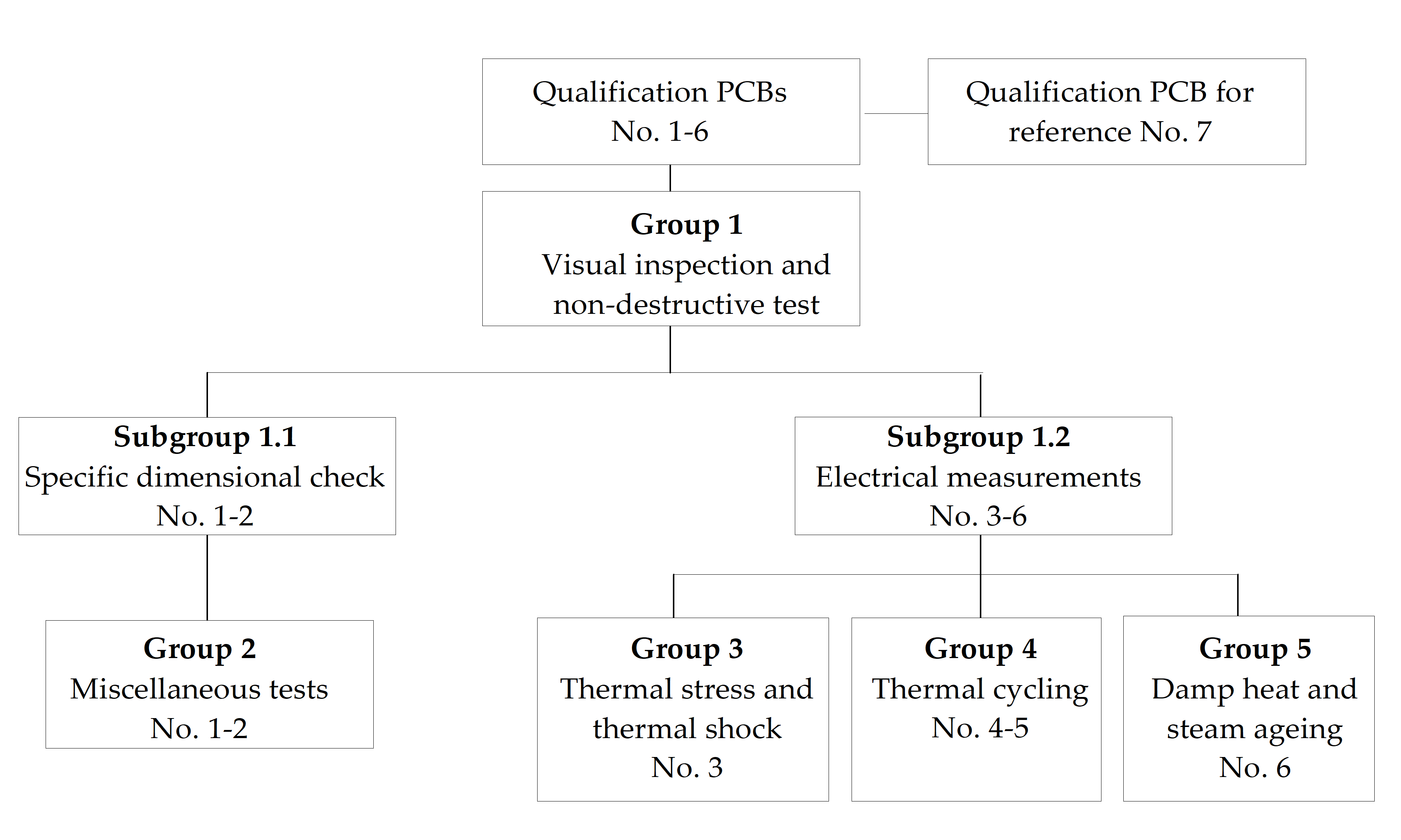 Figure 61: Test sequence
Table 61: Test specification
(Part 1 of 2)
|
Group
|
Tests
|
Clause
|
PCB no.Test pattern no.
|
|
Group 1
|
Visual inspection and nondestructive tests:
|
7.2
|
PCBs 1-6
|
|
Subgroup 1.1
|
Specific dimensional check
|
7.2.7
|
PCBs 1-2
|
|
Subgroup 1.2
|
Electrical measurements:
|
7.2.8
|
PCBs 3-6
|
|
Group 2
|
Miscellaneous tests
|
7.3
|
PCBs 1-2
|
|
Subgroup 2.1
|
Solderability test:
|
7.3.2
|
Test pattern J
|
|
Subgroup 2.2
|
Mechanical tests:
|
7.3.3
|
Test pattern B
|
|
Subgroup 2.3
|
Coating tests:
|
7.3.4
|
Test pattern G
|
|
Subgroup 2.4
|
Electrical tests:
|
7.3.5
|
Test pattern E
|
|
Subgroup 2.5
|
Physical tests:
|
7.3.6
|
Test pattern K
|
Table 61: Test specification
(Part 2 of 2)
|
Group 3
|
Thermal stress
|
7.4
|
PCB 3
|
|
Group 4
|
Thermal cycling
|
7.5
|
PCBs 4-5
|
|
Group 5
|
Damp heat — Steam ageing
|
7.6
|
PCB 6
|
|
a. i.e.: in the same layer.
| |||
Qualification PCBs
General
The qualification PCBs shall have test patterns that enable evaluation of the specific characteristics, summarised in Table 61 and described in detail in clause 7.
The qualification PCB shall represent the highest technological capability for which the PCB manufacturer applies for qualification.
The qualification PCB shall consist of a test pattern demonstrating the technological capability (test pattern L) together with the other test patterns.
The pattern drawing on layer 1 of the individual test patterns given below and shown as an example in Figure 62 can be used.
The PCB manufacturer and the qualification authority shall agree on the layout of the capability pattern.
The capability pattern can be an actual PCB circuit to be used in the space project.
The test pattern layout and design shall be in conformance with the referenced IEC specification if applicable:
- Single and double sided PCBs with platedthrough holes: IEC 60326-5.
- Rigid multilayer PCBs with interlayer connections: IEC 62326-4.
- Single and double sided flexible PCBs with through connections: IEC 60326-8.
- Flexrigid multilayer PCBs with through connections: IEC 60326-11.
The test pattern layout and design for sequentially laminated multilayer PCBs and special PCBs shall be agreed between PCB manufacturer, supplier and qualification authority.
 Figure 62: Example of a qualification PCB layout with patterns for testing and a pattern for demonstration of the technological capability
Test pattern A: Electrical test
The following measurements shall be performed on test pattern A:
- Intralayer insulation resistance.
- Dielectric withstanding voltage.
See example in Figure 63.
The conductor width and spacing within each layer shall represent the minimum dimensions to be qualified.
The comb pattern can provide a useful tool for evaluating cleanliness.
 Figure 63: Example of test pattern for intralayer insulation resistance and dielectric withstanding voltage testing
Test pattern B: Mechanical test
The following measurements shall be performed on test pattern B:
- Peel strength of copper track on laminate.
- Pulloff strength of surface mount pads.
- Surface solderability.
See example in Figure 64.

This is a surface pattern only and all holes are nonplatedthrough.
Figure 64: Example of test pattern for testing peel strength of conductors and pulloff strength of pads
Test pattern C: Electrical test
The internal short circuit shall be measured on test pattern C.
- 1 This consists in verifying the insulation between platedthrough holes in daisy chain through all layers and ground plane.
- 2 See example in Figure 65.
 Figure 65: Example of test pattern for internal short circuit testing
Test pattern D: Electrical test and visual aspect
The following measurements shall be performed on test pattern D:
- Marking.
- Etching definition.
- Continuity between platedthrough holes in daisy chain through all layers.
- Visual aspect.
See example in Figure 66.
 Figure 66: Example of test pattern for etching definition evaluation and continuity testing
Test pattern E: Electrical test
The following measurements shall be performed on test pattern E:
- Interconnection resistance between platedthrough holes in daisy chain through all layers before and after thermal cycling and thermal stress.
- Current overload between platedthrough holes in daisy chain through all layers for short and long duration.
See example in Figure 67.
 Figure 67: Example of test pattern for interconnection resistance and current overload testing
Test pattern F: Metalplating test
The following measurements shall be performed on test pattern F:
- Microsectioning to evaluate and determinate metal plating thickness.
- Microsectioning after thermal cycling, thermal stress and damp heat (optional).
See example in Figure 68.
 Figure 68: Example of test pattern for microsectioning and metal plating evaluation
Test pattern G: Metalplating/coating test
The following measurements shall be performed on test pattern G:
- Tape test for evaluation of adhesion of plated coating on copper track.
- Analysis of SnPb composition after reflow.
See example in Figure 69.
 Figure 69: Example of test pattern for plating adhesion testing and analysis of SnPb coating composition after reflow
Test pattern H: Electrical test
The following measurements shall be performed on test pattern H:
- Interlayer insulation resistance and dielectric withstanding voltage before and after thermal cycling and, optionally, after damp heat.
- Interlayer insulation resistance and withstanding voltage measured between platedthrough holes and a central ground plane.
See example in Figure 610.
 Figure 610: Example of test pattern for interlayer insulation resistance and dielectric withstanding voltage testing
Test pattern J: Solderability test
The following measurements shall be performed on test pattern J:
- Solder wettability of pads and platedthrough holes.
- Rework simulation on platedthrough holes.
See example in Figure 611.
 Figure 611: Example of test pattern for solder wettability and rework simulation testing
Test pattern K: Physical test
The following measurements shall be performed on test pattern K:
- Water absorption (optional).
- Outgassing tests on base laminate material according to ECSS-Q-ST-70-02.
See example in Figure 612.
 Figure 612: Example of test pattern for water absorption and outgassing testing
Test pattern L: Demonstration of technological capability
The following measurements shall be performed on test pattern L:
- Minimum conductor width.
- Minimum spacing.
- Minimum hole diameter.
- Other features that characterise the level of technological capability of the PCB design in terms of dimensional outline, build-up, non-standard use of materials.
See example in Figure 613.
 Figure 613: Example of test pattern for evaluation of the technological capability
Test pattern M: CAD/CAM criteria(on request by the qualification authority)
The CAD/CAM capability of the PCB manufacturer shall be evaluated on test pattern M by visual inspection.
See example Figure 614.
For this purpose the layout of the test pattern shall:
- be divided up into 3 zones with identical surfaces.
- have various pads in each zone (circular, oblong, square, rectangular).
- have a thermal shunt for internal layers.
 Figure 614: Example of test pattern for evaluation of CAD/CAM capability
Test pattern X: Resistance to bending cycles (for flexible parts only)
The following measurements shall be performed on test pattern X:
- Evaluation of continuity of conductors after exposing the pattern to bending cycles.
- Evaluation of adhesion between conductors and insulating material after exposing the pattern to bending cycles.
See example in Figure 615.
 Figure 615: Example of test pattern for testing resistance to bending cycles
Test pattern Y: Electrical test(on request by the supplier)
An impedance test shall be performed on test pattern Y.
See example Figure 616.
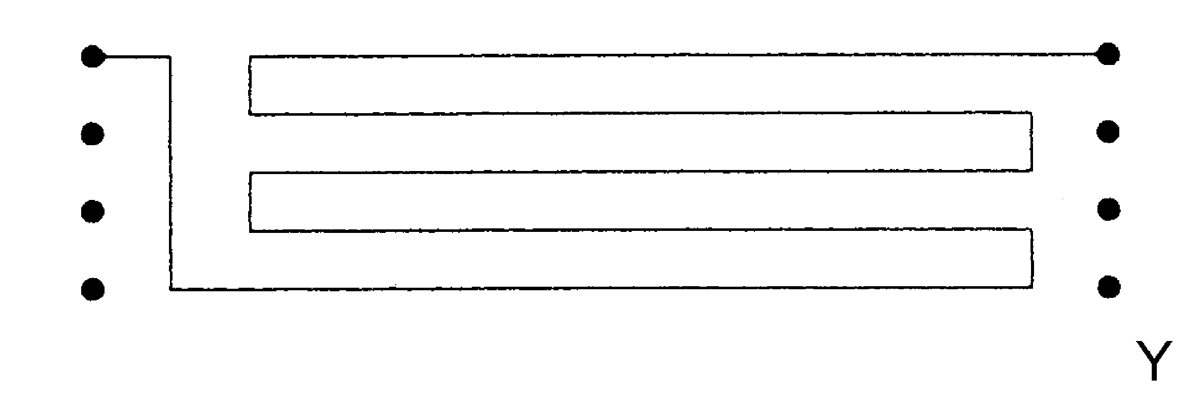 Figure 616: Example of test pattern for controlled impedance testing
Test pattern W: Electrical test for high frequency circuits (on request by the supplier)
The following measurements shall be performed on test pattern W:
- Dielectric constant.
- Loss tangent. The resonator for dielectric constant and loss tangent measurements shall be defined between PCB manufacturer and supplier.
This depends on the dielectric parameters of the material.
If the PCBs are used for manned space programmes the customer shall assure the PCB base material is tested for the following items:
- Flammability in conformance with ECSS-Q-ST-70-21.
- Offgassing (toxicity) and odour according to ECSS-Q-ST-70-29.
Qualification approval
The qualification authority shall grant qualification approval to the PCB manufacturer based on the examination and acceptance of the qualification programme.
The manufacturing process of the PCBs shall be established and documented in a PID in conformance with Annex C.
The qualification approval shall be valid for a period of two years.
Maintenance of qualification
During the period in which the qualification approval is valid the PCB manufacturer shall notify the qualification authority in case any problem arises that is related to the manufacturing of PCBs.
To maintain qualification status, the PCB manufacturer shall send, two months before the expiry date of the qualification period, the following items to the qualification authority:
- A qualification status report in conformance with Annex D.
- One recently manufactured high reliability PCB sample for technical assessment. Based upon the information received, the result of the technological examination and an investigation of the experiences regarding delivery times and quality of PCBs supplied for space projects, the qualification authority shall decide upon one of the following:
- In case there are no nonconformances, to extend the qualification period by two years and eventually to arrange a control visit to the PCB manufacturer’s plant.
- In case there are nonconformances, the necessary corrective action is negotiated with the PCB manufacturer in order to enable maintenance of qualification status.
This can include additional testing to be agreed between PCB manufacturer and qualification authority and submittal of a new PCB sample.
The PCB manufacturer shall arrange for an audit by the qualification authority every second year.
The qualification shall be withdrawn if the:
- submitted PCB specimen for qualification renewal is rejected;
- results of an audit at the manufacturing facility are unsatisfactory;
- materials or manufacturing processes are modified without prior authorization by the qualification authority;
- supplier has met major nonconformances regarding delivery time and manufacturing defects.
Tests
General
Unless otherwise specified, all tests shall be carried out under the below specified normal atmospheric conditions in conformance with test 18a of IEC 60326-2-am 1 (1992-06):
- Room temperature: (22 3) C.
- Relative humidity: (55 10) %.
- Atmospheric pressure.
Before testing is started, the PCBs shall be subjected for 48 h to ambient conditions.
During a sequence of measurements, the atmospheric conditions in the test area shall not undergo significant or rapid changes.
The PCBs to be tested shall not be covered with a protective varnish.
During the testing period, the following precautions shall be taken: - Keep the boards flat against a plane surface.
- Protect boards used for electrical tests from any contamination and hold them only by their edges during the tests.
- Before environmental exposure, soldering operation, electrical and mechanical testing, clean the boards in conformance with ECSS-Q-ST-70-08.
Group 1 — Visual inspection and nondestructive test
General
The PCBs number 1-6 shall be used for the tests.
Verification of marking
Each board shall be inspected with the naked eye for correct marking.
The marking shall be legible and resistant to test stresses.
The nonconformance criteria shall be as follows:
- Identification impossible M
- Marking not conforming to supplier’s specification M
- Defects not affecting identifications m
Visual aspects
Each board shall be inspected by magnification 10 with suitable lighting conditions to verify that construction and workmanship meet the requirements.
In case of any irregularity, the area shall be examined under 20 - 40 magnification.
The nonconformance criteria for the general cleanliness and contamination shall be as follows:
- Contamination visible to the naked eye and not removable by cleaning according to ECSS-Q-ST-70-08 M
- Contamination visible to the naked eye and removableby cleaning according to ECSS-Q-ST-70-08 m The nonconformance criteria for the substrate shall be as follows:
- Not in conformance with PCB manufacturer’s trademark and required quality M
- Scratches cutting glass fibre or leaving marks in the dielectric laminate that are affecting reliability M
- Scratches not affecting reliability m
- Dents, crazing and haloing:
- Visible to the naked eye M
- Only visible with magnification aids m
- Nonhomogeneity regarding colouring and opacity m/M
- Discoloured copper oxide layer on internal layer is acceptable;
- Inclusion of foreign matter, blistering or air bubbles:
- Visible to the naked eye M
- Only visible with magnification aids m
- Delamination M
- Measling:
- General measling spread over the whole PCB surface M
- Local measling that causes reduction of the insulation distance in the outer layer to below the requirement M
- Local measling that does not cause reduction of the insulation distance in the outer layer to below the requirement m
- Fungus growth M
- Delamination of cover layer (only for flexible PCB) m/M The nonconformance criteria for nonplatedthrough holes shall be as follows:
- Holes plated unintentionally m/M
- Incompletely drilled holes, missing or additional holes m/M The nonconformance criteria for the routing shall be as follows:
- Incomplete routing of board, such that dimensional or mechanical requirements are not met M
- Arbitrary cutting defects that remain acceptable within the dimensional requirements m The nonconformance criteria for the surface metallization shall be as follows:
- Conductors or pads not conforming to supplier’s specification M
- Terminal pads or conductors partially or completely missing M
- Terminal pads or conductors that are cut M
- Terminal pads or conductors forming a short circuit M
- Lifting/delamination of conductive pattern from substrate M
- Scratches in the SnPb metallisation exposing the underlaying copper plating M
- Copper or nickel visible on top surface plated areas M
Exposed copper can be accepted on the side of tracks or on the side of soldering pads.
- Large number of superficial scratches not attributed to a manufacturing process evidencing bad workmanship M
- Dewetting of fused tin lead finish on solder pads M
- Granular surface structure of fused tin lead finish on solder pads m/M
- Corrosion of exposed copper M
- Migration of underlaying copper through gold coating M The nonconformance criteria for platedthrough holes shall be as follows:
- Incompletely drilled, additional or missing holes M
- Partially or completely missing metallization M
- Component holes 0,6 mm filled or partially filled with solder resulting in a diameter smaller than the requirement m/M The nonconformance criteria for arbitrary defects of conductors and terminal pads shall be as follows:
- a 20 % of x and minimum conductor width requirement m
- a 20 % of x M
- minimum conductor width requirement M
- b x m
- b x M
- Opposite peaks: if z 80 % of y M
- Isolated peaks or valleys: h 20 % of x and z requirement M
- Conducting island: a + h 20 % of y and the isolation spacing requirement M
- Minimum remaining spacing y - a requirement M
- a 20 % of y M
- b y M
- Cover layer (flexible PCBs) covering part of solder pad (see Figure 73) M
Intermittent and irregular metallisation defects on conductors are edge roughness (peak or valley), pits, pin holes, voids, protrusions or indentations, as shown in Figure 71, Figure 72 and Figure 73.
 Figure 71: Arbitrary defects on conductors
Figure 72: Arbitrary defects on spacing between conductors
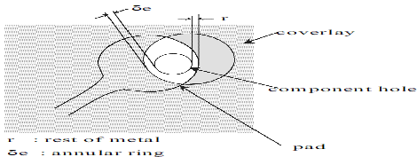 Figure 73 Misalignment of cover layer (for flexible PCBs)
External dimensions
Each board shall be measured by means of suitable standard measuring equipment to verify that the physical dimensions, including board thickness and external dimensions meet the supplier’s specification.
The nonconformance criteria for the thickness of base laminate (average of 4 measurements on the board) shall be as follows:
- Thickness not conforming to tolerance limits of the supplier’s specification M The nonconformance criteria for the length and width of board (average of 2 measurements on the board) shall be as follows:
- Length or width not conforming to tolerance limits of the supplier’s specification M
Warp
The PCBs shall be placed unrestrained on a plane horizontal surface with the convex side upward.
The warp shall be expressed in percentage terms.
The maximum bow between the plane horizontal surface and the PCB shall be measured as defined in Figure 74.
The length of the PCB shall be measured.
The warp percentage shall be calculated as defined in equation [71]:
|

|
[71]
|
The nonconformance criteria shall be as follows:
- Warp requirement M
 Figure 74: Warp
Twist
The PCB shall be placed on a plane horizontal surface so that it rests on three corners.
The twist shall be expressed in percentage terms.
The distance between the plane horizontal surface and the fourth corner of the PCB shall be measured as defined in Figure 75.
The length of the diagonal shall be measured.
The twist percentage shall be calculated as defined in equation [72].
|

|
[72]
|
The nonconformance criteria shall be as follows:
- Twist requirement M
 Figure 75: Twist
Subgroup 1.1 — Specific dimensional check
The PCBs number 1-2 shall be used for the tests.
The points to be measured on associated test coupons and PCB shall be decided between PCB manufacturer and qualification authority.
This can include for example:
- Minimum and maximum platedthrough holes diameter and soldering pads diameter.
- Minimum and maximum conductor width.
- Minimum and maximum distance between conductors.
The measurements shall be presented in tabular form.
An example is given in Figure 76.
The measurements of dimensional parameters relating to metal plating shall be taken at the copper/board base interface or for high frequency circuits as required by the supplier (see clause 7.3.4, Figure 78).
- 1 Examples for dimensional parameters relating to metal plating are width of conductors, spacing, minimum annular ring.
- 2 Hole diameters can be measured with measuring gauges or a measuring microscope.
|
Platedthrough holes
| |||||
|
Measuring point
|
Associated test coupon
|
pad
|
hole
| ||
|
Measured
|
Deviation
|
Measured
|
Deviation
| ||
|
Conductor’s widths
| |||
|
Measuring point
|
Test or coupon
|
Measured dimension
|
Deviation
|
|
Spacing between conductors
| |||
|
Measuring point
|
Test or coupon
|
Measured dimension
|
Deviation
|
Figure 76 Example of a presentation of measurements in tabular form
The nonconformance criteria shall be as follows:
- Dimensions not conforming to the circuit definitiondocument and acceptable tolerance limits of the supplier’s specification M
Example of such dimensions are diameter of holes, width of conductors and diameter of terminal pads.
- Diameter of nonsoldering holes not conforming to tolerance limits of the supplier’s specification m
Subgroup 1.2 — Electrical measurements
General
The PCBs number 3-6 shall be used for the tests.
Intralayer insulation resistance on test pattern A
The test shall be carried out in conformance with tests 6a and 6b of IEC 60326-2-am 1 (1992-06).
A direct voltage of (500 50) V shall be applied between the two closest conductors that are not electrically connected.
The insulation resistance (R) shall be measured 1 min after the voltage has been applied.
The nonconformance criteria shall be as follows:
- R requirement M
Interlayer insulation resistance on test pattern H
The test shall be carried out in conformance with test 6c of IEC 60326-2-am 1 (1992-06).
The test shall be carried out in conformance with clause 7.2.8.2.
The voltage shall be applied between two ground planes or between one ground plane and one conductor that are superimposed, i.e. on two separate adjacent layers.
The nonconformance criteria shall be as follows:
- R requirement M
Dielectric withstanding voltage intralayer on test pattern A and interlayer on test pattern H
The test shall be carried out in conformance with tests 7a and 7b of IEC 60326-2-am 1 (1992-06).
For interlayer measurements the test voltage shall be applied between two superimposed conductors (i.e. between layers).
For intralayer measurements the test voltage shall be applied between two adjoining, but not electrically connected conductors within the same layer.
The AC voltage at 50 Hz shall be gradually applied progressing from 200 V r.m.s. per second up to 1 500 V r.m.s. per mm of spacing between two conductors.
This voltage shall be kept steady for one minute.
The current shall be limited to 100 A.
The final evaluation shall be visual aspect and measurements of the continuity.
The nonconformance criteria shall be as follows:
- Evidence of breakdown, flashover or sparking M
Continuity on test pattern D
The test shall be carried out in conformance with test 3a of IEC 60326-2-am 1 (1992-06).
Conductor continuity shall be tested by measuring the interconnection resistance on test pattern D.
The measurement shall be performed using a method ensuring an error no greater than 5 % (four wire method).
The current shall be limited to 0,1 A.
The measuring voltage shall not exceed 5 V.
The posttest measurements taken on each sample shall be compared with pretest measurements.
The nonconformance criteria shall be as follows:
- Discontinuity M
- Dispersion greater than 10 % with respect to the mean of values measured on the test patterns m/M
Interconnection resistance on test pattern E
The test shall be carried out in conformance with test 3b of IEC 60326-2-am 1 (1992-06).
The test conditions shall be the same as for continuity testing.
The nonconformance criteria shall be as follows:
- Discontinuity M
- Dispersion greater than 10 % with respect to the mean of values measured on the test pattern M
Impedance test on test pattern Y
The test shall be carried out in conformance with test 9a of IEC 60326-2-am 1 (1992-06).
The measuring method shall be specified by the supplier.
Dielectric constant and loss tangent for high frequency materials on test pattern W
The measuring method shall be specified by the supplier:
- Annular ring;
- Closed cavity or other method.
Group 2 — Miscellaneous tests
General
The PCBs number 1-2 shall be used for the tests.
Subgroup 2.1 — Solderability test — Wettability on test pattern J
The test shall be carried out in conformance with test 14a of IEC 60326-2-am 1 (1992-06) and IEC 60068-2-20-am 2 (1987-01), test TC.
Nonactivated rosinbased flux shall be used as specified in ECSS-Q-ST-70-08.
The solder shall be tin-lead 60/40 or 63/37 as specified in ECSS-Q-ST-70-08.
The test machine shall be a rotary dip tester or similar equipment.
The specimens shall be fluxed by immersion.
Surplus flux shall be allowed to flow off the specimen by keeping it upright for 5 min.
The specimen shall be arranged on the soldering machine and brought into contact with the surface of the solder bath that is kept at the temperature of (235 5) C for the below specified period:
- For evaluation of wetting: 3 s.
- For evaluation of dewetting: 10 s. A visual inspection shall be made with a 10 magnification.
A microsection can also be performed and a visual inspection made at a magnification greater than 100.
The nonconformance criteria shall be as follows:
- Poor wettability of solder pads and platedthrough holes: see Figure 77 M
- Microsectioning: broken metallization M
 Figure 77: Wettability of terminal pads and platedthrough holes
Subgroup 2.2 — Mechanical tests
Peel strength on test pattern B
The test shall be carried out in conformance with test 10a of IEC 60326-2-am 2 (1992-06).
The conductor selected shall be peeled back at one end for a length of about 10 mm.
The detached end of the conductor shall be firmly gripped over its whole width.
Traction shall be applied in a direction perpendicular to the plane of the PCB until the copper starts to peel away.
The rate of traction shall be kept constant at 50 mm/min.
The traction direction shall be kept perpendicular to the plane of the PCB.
Machine inertia shall have no effect on the measurement.
The conductor width to be taken into account shall be the actual width over which the conductor is adhered to the substrate.
The nonconformance criteria for the peel strength shall be as follows:
- Peel strength requirement M
Pulloff strength on test pattern B
The test shall be carried out in conformance with test 11a of IEC 60326-2-am 1 (1992-06).
Temperature of iron shall be (270 10) C.
The solder shall be tinlead 60/40 or 63/37 alloy with noncorrosive resin core as specified in ECSS-Q-ST-70-08.
After application of the soldering flux specified in IEC 60068-2-20-am 2 (1987-01), test TC, the pads shall be tinned for (4 1) s.
A tinned copper wire with a diameter of 0,3 mm less than the hole diameter and with a length of approximately 150 mm shall be soldered onto the pad.
Soldering shall be between 2 s and 3 s.
After 5 min ambient reconditioning the soldering operations shall be repeated (second soldering).
The ambient reconditioning time before final measurement shall be more than 10 min.
For the measurement of the pull-off strength the following steps shall be carried out:
- Force is applied on the wire by using a traction machine.
- This force increases with a constant rate of between 5 N/s and 50 N/s until the terminal pad separates from the board base material.
The preferred rate is 10 N/s.
The nonconformance criteria for the pulloff strength for terminal pads shall be as follows:
- Pull-off strength requirement M
Flexural fatigue on test pattern X (only for double sided flexible PCB)
The test shall be carried out in conformance with test 21a of IEC 60326-2-am 1 (1992-06).
The equipment shall be similar to that described in IEC 60249-1-am 4 (1993-05) clause 3.12-2 and Figure 613.
Short insulated wires shall be connected to the ends of the conductive patterns (frontside and backside in series).
The specimen shall be mounted on the device such that the interior diameter of the loop is (9,6 0,4) mm.
The alternating movement shall be such that the loop moves at least 25 mm and that the specimen is not curved at either end.
The pace of the alternating movement shall not exceed ten cycles per minute.
For the test the alternating movement shall be continued until an electrical discontinuity appears or until 500 cycles are completed without defect.
The nonconformance criteria shall be as follows:
- Discontinuity occuring before 250 cycles M
- Discontinuity occuring between 250 cycles and 500 cycles m
- Lifting of insulation coating from conductors m/M
- Lifting of conductors from board base material m/M
- Lifting of insulation coating from board base material m/M
Bending test (only for rigidflex)
The test shall be carried out in conformance with MIL-P-50884C clause 3.6.5 and 4.8.4.5.
A 25 cycle folding test shall be carried out as described in MIL-P-50884C clause 4.8.4.5.
There shall be no electrical defect or degradations.
The nonconformance criteria shall be as follows:
- Any degradation of continuity M
Subgroup 2.3 — Coatings tests
Coating adhesion of nonfused SnPb finishes on test pattern G
The test shall be carried out in conformance with test 13a of IEC 60326-2-am 1 (1992-06).
The test shall be carried out on SnPb finished boards before reflow of test board.
After cleaning, an adhesive tape, at least 50 mm long, shall be applied to the test surface and pressed down to eliminate all air bubbles.
After 10 s, the tape shall be quickly pulled off perpendicular to the coating surface.
The surface area to be tested shall be 1 cm2 of conductor
Example of tape, which can be used: TESA 4104 width 19 mm.
The nonconformance criteria shall be as follows:
- If part of SnPb coating is sticking to tape or test surface shows scaling M
Analysis of SnPb coating on test pattern G
The tinlead alloy shall be chemically dissolved.
The relative quantities of tin and lead shall be determined by atomic absorption spectrometry.
This is the proposed method for SnPb. Any other method resulting in the same degree of precision can be used.
The nonconformance criteria shall be as follows:
- If the content of tin and lead is not conforming to the tolerance limits of the requirement M
Microsectioning on test pattern F
General
The test shall be carried out in conformance with tests 1c and 15b of IEC 60326-2-am 1 (1992-06).
For high frequency conductors the customer shall specify at which height of the conductor the width shall be measured (see Figure 78).
Microsection with typical defects in PTH is shown in Annex F.
 w width of conductor
e minimum annular erring on external layer
e minimum annular erring on internal layer
d diameter of plated-through hole
h height of conductor
Figure 78: Dimensional parameters to be measured
Thickness of metalplating
The test shall be carried out on a microsection.
Observations shall be made with magnification greater than or equal to 250.
The nonconformance criteria for the thickness of copper plating on external layers shall be as follows:
- Basic copper:
- Thickness not conforming to the supplier’s specification M
- Basic copper plus electrolytic copper on nonsoldering areas:
- Thickness requirement M
- Basic copper plus electrolytic copper soldering pads (see Figure 79 number 2):
- Thickness 40 m M
The nonconformance criteria for the thickness of copper in platedthrough holes that are component holes shall be as follows:
- Thickness 40 m M
- Average thickness based on 3 measurements taken on the hole walls (see Figure 79 number 1):
- Thickness requirement M
The nonconformance criteria for the thickness of copper layer on internal layers shall be as follows:
- Thickness requirement M
- Thickness not conforming to supplier’s specification M The nonconformance criteria for the thickness of copper in platedthrough holes that are vias, buried vias or blind vias shall be as follows:
- Thickness requirement M The nonconformance criteria for the thickness of tinlead alloy on surface, measured along the conductor longitudinal axis, shall be as follows:
- 5 m thickness 8 m m
- Thickness 5 m M The nonconformance criteria for the thickness of tinlead alloy in holes shall be as follows:
- In highest part of half of the hole wall height(see Figure 79 number 3): thickness 8 m M
- On angle of hole corner (see Figure 79 number 4):1 m thickness 2 m m
- On angle of hole corner (see Figure 79 number 4):thickness 1 m M The nonconformance criteria for the thickness of electrolytic Au or Au/Ni on surface and in holes (measured along the conductor longitudinal axis) shall be as follows:
- Au for manual soldering on nickel:
- Thickness 1 m M
- Thickness 7 m M
- Au for manual soldering on copper:
- Thickness 3 m M
- Thickness 7 m M
- Au for high frequency circuits or other assembly methods as specified by customer:
- Thickness not conforming to tolerance limits of supplier’s specification M
- Ni:
- Thickness 2 m M
- Thickness 10 m M
The nonconformance criteria for the distance between SnPb and Au overlap and the termination pad designated for soldering shall be as follows:
- Distance 200 m M The nonconformance criteria for the etch undercut on external and internal layers for fused SnPb (see Figure 710) shall be as follows:
- Undercut (u) total copper thickness (h) M The nonconformance criteria for the etch undercut on external and internal layers for Au plating with or without Ni finish (see Figure 711) shall be as follows:
- If undercut (d) 30 m M The nonconformance criteria for the etch overhang on external layers for Au plating with or without Ni finish (see Figure 712) shall be as follows:
- If overhang (D) 2 thickness of total copper M
For high frequency application overhang is normally undesirable and can be removed mechanically.
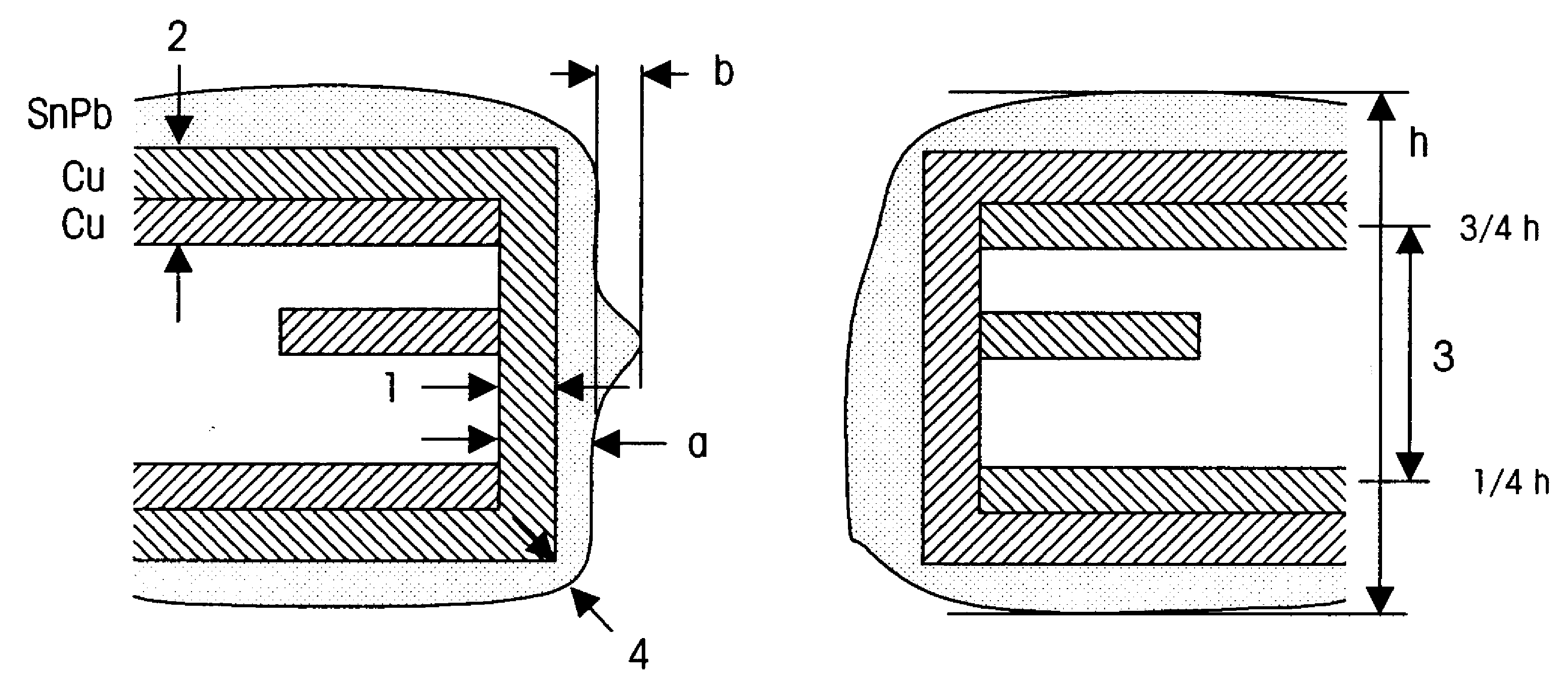 Key
Key
1 = Cu in PTH
2 = Cu at surface pattern
3 = SnPB in hole
4 = SnPb in angle area
internal buging b < a
Figure 79: Microsection of a PTH
 Figure 710: Undercut for PCBs with fused SnPb finish
 Figure 711: Undercut for PCBs with Au/Ni or Au finish
 Figure 712: Overhang for PCBs with Au/Ni or Au finish
Aspect of platedthrough holes
Sections of platedthrough holes shall be observed with magnification greater than or equal to 100.
Layer misregistration compared to the minimum annular ring on pads.
The nonconformance criteria for the layer misregistration on the external layer (see Figure 78) shall be as follows:
- e requirement M The nonconformance criteria for the layer misregistration on the internal layers (see Figure 78) shall be as follows:
- i requirement M
- Minimum insulation between layers requirement M The nonconformance criteria for irregular drilling (see Figure 713) shall be as follows:
- Infiltration of metal into base laminate:
- 40 m infiltration 80 m m
- Infiltration 80 m M
- Presence of adhesive on basic copper not leading to rupture during fusing process or thermal shock m
- Adhesion defects between metalplating and basic copper M
- Adhesion defects between metalplating and inner layers M
- Resin smear on the interface between internal conductor and plated copper greater than 15 % of conductor thickness M
- Void in resin greater than 50 % of basic copper thickness M The nonconformance criteria for voids in PCB base laminate substrate and resin recession in holes (see Figure 714) shall be as follows:
- Voids in the PCB base laminate substrate:
- Lc 80 m M
- At edge of metalplating:
- Sum of resin recession hc 20 % sum hi M
- Resin recession in hole before or after test:
- Resin recession between 10 % and 20 % of height of hole m
- If resin recession 20 % of height of hole M
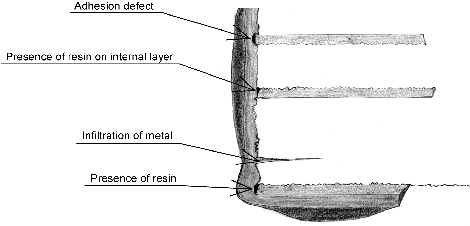 Figure 713: Microsection in PTH: Possible defects
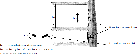 Figure 714: Microsection of PTH: Possible defects
The nonconformance criteria for the copper plating inside buried, blind, via and component holes shall be as follows:
- Void in copper plating in holes M
The nonconformance criteria for the resin inside buried vias shall be in conformance with Figure 715.
 Figure 715: Voids in resin inside buried vias
Subgroup 2.4 — Electrical tests
Current overload on test pattern E
General
The test shall be carried out in conformance with test 5 of IEC 60326-2-am 1 (1992-06).
Shorttime overload
The test shall be carried out on a pattern including holes (50 holes minimum) connected in series by conductors.
Two connecting wires shall be soldered to both ends of the circuit being tested.
A measurement shall be taken of the interconnection resistance between the ends.
Voltage shall be applied between ends in such a way that current flow into the circuit is:
- 7 A for 35 m thick basic copper.
- 14 A for 70 m thick basic copper.
This voltage shall be maintained for (4 1) s.
After ambient reconditioning for 2 h, circuit continuity shall be checked by measuring the interconnection resistance.
The nonconformance criteria shall be as follows: - Electrical discontinuity M
- Blistering visible to the naked eye M
- Variation in interconnection resistance increased by more than +10 % M
Longtime overload
Same initial conditions as in clause 7.3.5.1.2 with application of a voltage to the circuit terminals such that the current varies by successive steps:
- I0 = 2 A for 3 min.
- I1 = 4 A for 3 min;
- Further increments of 2 A every 3 min until destruction (open circuit) or if for I = 18 A circuit discontinuity is not achieved. The nonconformance criteria shall be as follows:
- destructive current requirement M
Internal short circuit on test pattern C
The test shall be carried out in conformance with test 4a of IEC 60326-2-am 1 (1992-06).
The test shall be carried out in an insulation area in conformance with Figure 716.
A polarized voltage of 100 V DC shall be applied between the ground plane connected to earth and the platedthrough hole passing through the access opening for 1 min (see Figure 716).
The insulation resistance shall be measured.
The nonconformance criteria shall be as follows:
- Insulation resistance requirement M
 Figure 716: Test for internal short circuit
Subgroup 2.5 — Physical tests on test pattern K
Water absorption (optional)
The specimen, completely devoid of copper, shall be dried in an oven for (24 1) h at a temperature between 50 C and 55 C.
It shall be cooled in a container with a siccative until the temperature is (23 1) C.
At this stage it shall be weighed to the nearest milligram.
It shall be placed in a deionized water bath maintained at (23 0,5) C.
It shall be placed on the edge, remain completely submerged and not in contact with the edges of the bath.
After (24 1) h, it shall be withdrawn from the water and dried with a dry flufffree cloth or filter paper.
It shall be weighed to the nearest milligram in the minute following its removal from the water.
The nonconformance criteria for the percentage of absorbed water (m) in various types of substrates shall be as follows:
- Glass fibreepoxy base laminate: m 0,2 % M
- Glass fibrepolyimide base laminate: m 0,8 % M
- Random glass reinforced PTFE resin: m 0,2 % M
- Ceramic filled wovenglass reinforced PTFE resin: m 0,1 % M
- Ceramic filled PTFE resin: m 0,1 % M
- Ceramic filled cross-linked hydrocarbon/thermoset polymer: m 0,1 % M
- Quartz filled polyimide: m 0,8 % M
- Polyimide: m 0,8 % M
Outgassing
The test shall be carried out in conformance with ECSS-Q-ST-70-02.
The test shall be carried out on a specimen entirely devoid of copper in order to determine the volume of included gas constituents, which threaten to contaminate a space environment.
The outgassing shall be determined after measurement of the difference in weight of the specimen before and after the test.
The nonconformance criteria shall be as follows:
- TML or RML 1 % (see ECSS-Q-ST-70-02 clause 7.2.3) and CVCM 0,1 % M
Group 3 — Thermal stress and thermal shock (on PCB)
General
The PCB number 3 shall be used for the tests.
PCB manufacturer and the qualification authority shall agree on omission of any of these tests.
The solder bath test is to simulate solder wave assembly of PCBs and is followed by the vapour phase solder test to simulate solder reflow assembly of PCBs. The rework test simulates hand solder assembly, rework and repair of PCBs.
Solder bath float and vapour phase reflow simulation (on board without test pattern F)
Solder bath floating test
The test shall be carried out in conformance with test 19c of IEC 60326-2-am 1 (1992-06).
The thermal shock shall be applied to one side of the test board by floating it in a solder bath.
After conditioning for 6 h at (140 2) C, the board shall be floated in a 63/37 solder bath maintained at (287 6) C.
The duration of the test shall be 10 s.
Ambient reconditioning shall be more than 1 h, after which a visual inspection shall be performed to evaluate the substrate visual aspect.
Vapour phase simulation test
The test shall be carried out in conformance with test 19g of IEC 60326-2-am 1 (1992-06).
A thermal shock shall be applied to the whole board of the test board by immersion in the vapour phase of a fluorinated chemical bath.
Depending on the time passed after the first thermal shock (during the solder bath float test), the board shall be conditioned for 1 h to 6 h at (140 2) C.
The other side compared to the procedure in 10.2.1.2a of the same test board shall be coated with flux or a solder paste with flux and baked.
The test board shall be lowered into the vapour phase at a temperature of (215 2) C.
The duration of the exposure shall be 10 s.
Ambient reconditioning shall be more than 1 h, after which the following final measurements shall be performed:
- Substrate visual aspect;
- Peel strength on test pattern B;
- Continuity on test pattern D;
- Interconnection resistance on test pattern E;
- Microsectioning on test pattern J. The nonconformance criteria shall be as follows:
- Peel strength requirement M
- Delamination M
- Localized/generalized measling m/M
- General occurrence of terminal pads that showfirst signs of pad lifting M
- Any terminal pad that show pad lifting M
- Increase in interconnection resistance +10 % M
- Microsectioning: broken metallization M
Rework simulation (thermal shock, hand soldering) on test pattern F
The test shall be carried out in conformance with test 19d of IEC 60326-2-am 1 (1992-06).
A thermal shock shall be applied to the test pattern F by soldering and unsoldering a wire five times.
Copper wires shall be of diameter:
- 0,51 mm for holes of = 0,8 mm ( of land = 2 mm).
- 1,02 mm for holes of = 1,6 mm ( of land = 4 mm).
A sufficient wire length to fit the gripping mechanism of the tensile tester shall be prepared for each hole.
The wires shall be inserted in the holes and soldered to the terminal areas using a conventional soldering iron, operating at a tip temperature of (270 10)� C.
The wires shall not be clinched on the other side of the PCB.
They shall be soldered and then unsoldered and removed from the hole.
This cycle shall be repeated five times, using a new wire for each soldering operation.
During the soldering/unsoldering cycles, the soldering iron shall be applied to the wire and not to the terminal pads.
After the fifth cycle, the wires shall be soldered into the holes and the PCB shall be left to cool for 30 min minimum.
A microsection shall be performed on the soldered holes to evaluate possible cracking of the copper of the throughhole plating.
The nonconformance criteria shall be as follows: - Cracked copper M
Group 4 — Thermal cycling (on PCB)
The PCBs number 4-5 shall be used for the tests.
The test shall be carried out in conformance with test Nb of IEC 60068-2-14-am 1 (1986-01).
The test is performed on an entire PCB.
The temperature range T shall be 200 C with the highest temperature not exceeding the glass transition temperature of the substrate.
The lower temperature can be (70 15) C.
The number of cycles shall be 200.
The temperature change rate shall be approximately 10 C/min.
The conditioning time at the extreme temperatures within a cycle shall be 15 min.
After ambient reconditioning for at least 2 h, the following final measurements shall be performed:
- Substrate visual aspect.
- Peel strength on test pattern B.
- Continuity on test pattern D and interconnection resistance on test pattern E.
- Intra and interlayer insulation resistance on test pattern A and H.
- Withstanding voltage on test patterns A and H.
- Microsectioning on test pattern F. The nonconformance criteria shall be as follows:
- Peel strength requirement M
- Increase in resistance +10 % M
- Intralayer insulation resistance 103 M M
- Interlayer insulation resistance 104 M M
- Evidence of flashover, breakdown, sparking M
- Microsectioning: broken metallization M
- Technological and functional defects M
Group 5 — Damp heat — Steam ageing (on PCB)
General
The PCB number 6 shall be used for the tests.
Damp heat (on entire PCB excluding test pattern F)
The test shall be carried out in conformance with test Ca of IEC 60068-2-3 (1969-01).
The test conditions shall be:
- Temperature: (40 2) C.
- Relative humidity: 93 % (+2 %, 3 %).
- Duration of test: 10 days.
- No operation during test. The sample shall be reconditioned to normal atmospheric conditions for a period of at least 1 h and not more than 2 h, after which the following final measurements shall be taken:
- Peel strength on test pattern B.
- Intra and interlayer insulation resistance on test patterns A and H.
- Withstanding voltage on test patterns A and H.
- Microsectioning (if necessary) on test pattern F.
- Corrosion of circuits for electrolytic Au finish. The nonconformance criteria shall be as follows:
- Peel strength requirement M
- Intralayer insulation resistance 103 M M
- Interlayer insulation resistance 104 M M
- Evidence of flashover, breakdown, sparking M
- Microsectioning (if required): broken metallization M
- Evidence of corrosion M
Steam ageing on test pattern F
The test shall be carried out in conformance with test 20a of IEC 60326-2-am 1 (1992-06).
This test is intended to give an indication of the effects of storage on the solderability of the PCBs.
The flux shall be nonactivated, rosinbased flux as specified in ECSS-Q-ST-70-08.
The solder shall be tinlead 60/40 or 63/37 alloy with noncorrosive resin core as specified in ECSS-Q-ST-70-08.
The test machine shall be a steam generator or similar equipment.
The specimens shall be fluxed by immersion.
Surplus flux shall be allowed to flow off the specimen by keeping it upright for 5 min.
The specimen shall be exposed in the steam generator machine for approximately 80 min.
After closing the generator, it shall be purged with nitrogen at a flow rate between 250 ml/min and 750 ml/min.
The specimen carrier shall rotate at a speed of 5 revolutions per minute to 50 revolutions per minute.
The temperature inside machine shall be (100 2) C and stabilized for (5 1) min.
The nitrogen flow shall be switched off.
The 90 C condensed steam rate in the chamber shall be controlled to (5 0,5) l/min.
A mixture of pure oxygen 20 % and nitrogen 80 % with a flow rate of (100 10) ml/min shall be switched on for (60 5) min.
After removing the specimens from the steam generator machine, they shall be dried.
A solderability test shall be performed.
A visual inspection shall be performed with a 10 magnification.
If the result of the visual inspection is deemed unsatisfactory, a microsection shall be performed. In this case a visual inspection shall be made with a magnification greater than 100.
The nonconformance criteria shall be as follows:
- Poor wettability of conductors, terminal pads and platedthrough holes: see Figure 77 for terminal pads and platedthrough holes M
- Microsectioning (if necessary): broken metallization M
- Evidence of corrosion M
Quality assurance for manufacturing
General
The quality assurance requirements defined in ECSS-Q-ST-20 shall apply.
No repair shall be performed on finished bare PCBs.
Data
The supplier shall retain the quality records for at least ten years or in accordance with project business agreement requirements.
Example of such quality records are logbooks.
The quality records shall be composed of the following:
- Documentation of the final inspection of manufactured PCBs.
- Nonconformance reports and corrective actions in conformance with ECSS-Q-ST-10-09;
- Copy of the test results (including evaluation and qualification test report) in conformance with Annex A and Annex B.
Incoming inspection of raw materials
Raw materials and semifinished products shall be selected, inspected and tested (e.g. chemical and physical tests) in conformance with the production flow chart.
The PCB manufacturer shall separate and, and prevent the use of, raw materials and semifinished products that are awaiting completion of test results.
Traceability
The PCB manufacturer’s control system shall make it possible to determine, in respect of any lot of PCBs, the history of all raw materials and semifinished products listed in the production flow chart and the individual process steps mentioned herein, and to verify that the items originate from one production lot.
In the case of materials with limited shelflife, the PCB manufacturer’s control system shall provide for means to verify the validity of the relevant material for use.
The verification and recertification procedure shall be in accordance with ECSS-Q-ST-70-22.
Calibration
The PCB manufacturer shall calibrate any electrical and mechanical manufacturing equipment to traceable reference standards.
The PCB manufacturer shall record any suspected or actual equipment failure as a nonconformance report according to ECSS-Q-ST-20.
This is to ensure that previous manufacturing results are examined to ascertain whether or not a reinspection or retesting is necessary.
Workmanship standards
Visual standards consisting of photos or drawings of microsections or other visual aids that clearly illustrate the quality characteristics required shall be available to each inspector.
Inspection
During all stages of the manufacturing the inspection points shall be observed. Quality conformance inspection shall be performed using quality test specimen and microsections.
Operator and inspector training
All operators and inspectors shall be suitably trained for their task and for the understanding of the necessary quality assurance requirements.
Quality test specimen
The PCB manufacturer shall produce with each panel quality test specimens for inhouse quality control purposes and one to be supplied to the qualification authority in accordance with ECSS-Q-ST-70-11 clause 5.5.1.
Microsection
The PCB manufacturer shall produce with each panel microsections for inhouse quality control purposes and one to be supplied to the qualification authority in accordance with ECSS-Q-ST-70-11 clause 5.5.2.
Final inspection and tests
The PCB manufacturer shall have an inhouse procedure for final inspection of PCBs; this shall include visual inspection according to clause 7.2 and specific dimensional check according to clause 7.2.7 and the qualification authority’s requirements.
Electrical testing shall be agreed between PCB manufacturer and the qualification authority in accordance with ECSS-Q-ST-70-11 clause 5.5.2.
The quality test specimen representative of the PCB and produced on the same panel shall be subjected to continuity test, solderability test and thermal stress test.
Other specific test can be agreed with the customer.
Microsectioning of holes as received and after thermal stress tests (rework simulation) shall be performed.
The PCBs shall be cleaned and dried before packaging according to ECSS-Q-ST-70-11 clause 5.4.2.
The cleanliness values shall be in accordance with ECSS-Q-ST-70-08 clause 11.3.
Delivery
The PCB manufacturer shall have suitable packaging facilities in conformance with ECSS-Q-ST-70-11 clause 5.4.
The documentation shall be done in conformance with ECSS-Q-ST-70-11 clause 5.3.3.
Requirements for PCBs
Rigid singlesided and doublesided PCBs
The base materials shall be in conformance with ECSS-Q-ST-70, IEC specifications and IPC-4101 and shall be one of the following:
- Woven-glass-reinforced epoxy resin FR4;
- Woven-glass-reinforced polyimide resin. The limits for the dimensional characteristics shall be as follows:
- External dimension tolerance: 0,2 mm;
- Thickness tolerance: 10 %;
- Active board size, maximum: supplier’s specification;
- Board thickness maximum: 3,2 mm;
- Positioning tolerance between registration mark and edge of circuit: 0,2 mm;
- Conductor width: 200 m minimum (for fine pitch 120 m width is tolerated if less than 5 mm from component pad);
- Spacing between conductors: 300 m minimum (for fine pitch 150 m spacing is tolerated if less than 5 mm from component pad);
- Conductor tolerance (minimum/maximum): supplier’s specification, 20 % maximum;
- Tolerance on diameter of terminal pads: supplier’s specification, 20 % maximum;
- Minimum hole diameter:
- Component hole: in conformance with ECSS-Q-ST-70-08;
- Via hole: 0,25 mm minimum and maximum aspect ratio t/d = 6;
- Tolerance on diameter of platedthrough holes:
- Nominal 0,7 mm: maximum 0,15 mm for component hole;
- Nominal 0,7 mm: maximum 0,20 mm;
- Tolerance on diameter of nonplatedthrough holes: maximum 0,20 mm;
- Positioning tolerance of holes with respect to reference mark: 0,1 mm;
- Relative misregistration pad/hole: 0,15 mm;
- Misalignment determined by measuring minimum annular ring:
- Solder side: 0,20 mm;
- Component side (reduced pads): 0,10 mm;
- Nonsoldering hole: 0,10 mm.
The limits for the electrolytic coatings shall be as follows:
- Electrolytic copper plating:
- Minimum purity: 99,5 %;
- Thickness of surface pattern: 25 m;
- Thickness of platedthrough holes: 25 m;
- Thickness of via holes: 20 m;
- Tin lead plating after reflow:
- Tin content of alloy: (63 8) %;
- Thickness on surface: 8 m in highest part;
- Thickness in platedthrough holes: 8 m in highest part (minimum half height of hole wall);
- Thickness on corner angle: 2 m;
- Electrolytic gold plating:
- Minimum purity: 99,8 % (not more than 0,2 % silver);
- Thickness on nickel: (4 3) m;
- Thickness on copper: (5 2) m;
- Electrolytic nickel plating:
- Thickness: 2 m to 10 m.
It is optional under gold.
The limits for the mechanical characteristics shall be as follows:
- Warp and twist: 1,1 % for board thickness 1,6 mm, 1,5 % for board thickness 1,6 mm;
- Conductor adhesion/peel strength:
- On epoxy: 16 N/cm;
- On polyimide: 12 N/cm;
- Pull strength:
- For terminal pads 4 mm on epoxy: 140 N;
- For terminal pads 4 mm on polyimide: 80 N;
- For terminal pads 2 mm on epoxy: 35 N;
- For terminal pads 2 mm on polyimide: 20 N.
The limits for the electrical characteristics shall be as follows:
- Insulation resistance:
- Intralayer (i.e. in the same layer): 104 M;
- Interlayer (i.e. between opposite layers): 105 M;
- Withstanding voltage per mm spacing between conductors:
- Intralayer and interlayer: 1 000 V r.m.s;
- Short time overload:
- 0,035 mm copper thickness: 7 A for 4 s;
- 0,070 mm copper thickness: 14 A for 4 s;
- Long time overload, destructive current:
- 0,035 mm copper thickness: I 8 A;
- 0,070 mm copper thickness: I 16 A.
Rigid singlesided and doublesided PCBs for high frequency application
The base materials shall be in conformance with ECSS-Q-ST-70, IEC specifications and IPC-4101 and shall be on of the following:
- Randomglassreinforced PTFE resin with or without Al backing;
- Wovenglassreinforced PTFE resin;
- Ceramic filled wovenglassreinforced PTFE resin;
- Ceramic filled PTFE resin with or without Al backing;
- Ceramic filled cross-linked hydrocarbon/thermoset polymer;
- Wovenglassreinforced epoxy resin FR4;
- Quartz filled polyimide resin. The limits for the dimensional characteristics shall be as follows:
- External dimension tolerance: 0,2 mm;
- Thickness tolerance: 10 %;
- Active board size, maximum: supplier’s specification;
- Board thickness (minimum/maximum): customer’s and supplier’s specification according to electrical performance;
- Positioning tolerance between registration mark and edge of circuit: 0,2 mm;
- Conductor width/spacing: customer’s and supplier’s specification according to electrical performance;
- Tolerance on conductor (minimum/maximum): supplier’s specification;
- Tolerance on diameter of terminal pads: customer’s and supplier’s specification according to electrical performance;
- Minimum hole diameter:
- Component hole: in conformance with ECSS-Q-ST-70-08;
- Via hole: 0,25 mm minimum and maximum aspect ratio t/d = 6;
- Tolerance on diameter of platedthrough holes:
- Nominal 0,7: maximum 0,15 mm for component hole;
- Nominal 0,7: maximum 0,20 mm;
- Tolerance on diameter of nonplatedthrough holes: maximum 0,20 mm;
- Positioning tolerance of holes with respect to reference mark: 0,1 mm;
- Relative misregistration pad/hole: 0,15 mm;
- Misalignment determined by measuring minimum annular ring:
- Solder side: 0,2 mm;
- Component side (reduced pads): 0,1 mm;
- Nonsoldering hole: 0,1 mm.
The limits for the electrolytic coatings shall be as follows:
- Electrolytic copper plating:
- Minimum purity: 99,5 %;
- Thickness of surface pattern for soldering pads: 25 m (total thickness of basic plus electrolytic copper 40 m);
- Thickness of platedthrough holes: 25 m;
- Thickness of via hole: 20 m;
- Tin lead plating after reflow:
- Tin content of alloy: (63 8) %;
- Thickness on surface: 8 m in highest part;
- Thickness in platedthrough holes: 8 m in highest part (minimum half height of hole wall);
- On corner angle: 2 m;
- Electrolytic gold plating:
- Minimum purity: 99,8 %
- Not containing more than 0,2 % silver;
- Thickness on nickel: 1 m to 7 m;
- Electrolytic nickel plating:
- Thickness: 2 m to 10 m;
It is optional under gold.
The limits for the mechanical characteristics shall be as follows:
- Warp and twist:
- Randomglassreinforced PTFE resin: n.a.;
- Wovenglassreinforced PTFE resin: n.a.;
- Ceramic filled PTFE resin: 1,1 %;
- Ceramic filled xlinked hydrocarbon/thermoset polymer: 1,1 %;
- Wovenglassreinforced epoxy resin FR4: 1,1 % for board thickness 1,6 mm, 1,5 % for board thickness 1,6 mm;
- Quartz filled polyimide: 1,1 % for board thickness 1,6 mm, 1,5 % for board thickness 1,6 mm;
- Conductor adhesion/peel strength:
- On PTFE reinforced/ceramic filled or nonfilled: 8 N/cm;
- Cross-linked hydrocarbon: 8 N/cm;
- On epoxy: 16 N/cm;
- On polyimide quartz: 12 N/cm;
- Pull strength:
- For terminal pads 4 mm on PTFE reinforced/ceramic filled or nonfilled: 60 N;
- For terminal pads 4 mm cross-linked hydrocarbon: 60 N;
- For terminal pads 4 mm on epoxy: 140 N;
- For terminal pads 4 mm on polyimide quartz: 60 N;
- For terminal pads 2 mm on PTFE reinforced /ceramic filled or nonfilled: 12 N;
- For terminal pads 2 mm cross-linked hydrocarbon: 12 N;
- For terminal pads 2 mm on epoxy: 35 N;
- For terminal pads 2 mm on polyimide quartz: 20 N.
The limits for the electrical characteristics shall be as follows:
- Insulation resistance:
- Intralayer: 104 M;
- Interlayer: 105 M;
- Withstanding voltage per mm spacing between conductors:
- Intralayer and interlayer: 1 000 V r.m.s.;
- Short time overload:
- 0,009 mm copper thickness: n.a.;
- 0,017 mm copper thickness: n.a.;
- 0,035 mm copper thickness: 7 A for 4 s;
- 0,070 mm copper thickness: 14 A for 4 s;
- Long time overload, destructive current:
- 0,009 mm copper thickness: n.a.;
- 0,017 mm copper thickness: n.a.;
- 0,035 mm copper thickness: I 8 A;
- 0,070 mm copper thickness: I 16 A;
- Permittivity: customer’s and supplier’s specification according to electrical performance;
- Loss angle Tg customer’s and supplier’s specification according to electrical performance.
Flexible PCBs
The base materials shall be in conformance with ECSS-Q-ST-70, IEC specifications and IPC-4101 and shall be the following:
- Flexible copperclad polyimide film. The limits for the dimensional characteristics shall be as follows:
- External dimension tolerance: 0,4 mm;
- Thickness tolerance: 20 %;
- Active board size, maximum: supplier’s specification;
- Board thickness maximum: 0,4 mm;
- Positioning between registration mark and edge of circuit: 0,4 mm;
- Conductor width/spacing: (250 m/250 m) minimum;
- Conductor tolerance (minimum/maximum): supplier’s specification;
- Tolerance on diameter of terminal pads: supplier’s specification;
- Minimum diameter of platedthrough holes: 0,25 mm;
- Tolerance on diameter of platedthrough holes for components:
- Nominal 0,7: maximum 0,15 mm;
- Nominal 0,7: maximum 0,20 mm;
- Tolerance on diameter of nonplatedthrough holes: maximum 0,20 mm;
- Positioning of holes with respect to reference mark: 0,10 mm;
- Relative misregistration pad/hole: 0,15 mm;
- Registration of sides: 0,10 mm;
- Cutting of insulation coating tolerance:
- Internal cutting: 0,50 mm;
- Misalignment determined by measuring minimum annular ring:
- Solder side: 0,25 mm;
- Reduced terminal pads (oblong): 0,10 mm;
- Nonsoldering holes: 0,10 mm;
- Misalignment of insulation coating determined by measuring rest of metal:
- Platedthrough holes: 0,15 mm;
- Nonplatedthrough holes: 0,25 mm;
- Number of layers: 2. The limits for the electrolytic coatings shall be as follows:
- Electrolytic copper plating:
- Minimum purity: 99,5 %;
- Thickness of surface pattern: 25 m;
- Thickness of platedthrough holes: 25 m;
- Tin lead plating after reflow:
- Tin content of alloy: (63 8) %;
- Thickness on surface: 8 m in highest part;
- Thickness in platedthrough holes: 8 m in highest part (minimum half height of hole wall);
- On corner angle: 2 m.
The limits for the mechanical characteristics shall be as follows:
- Conductor adhesion/peel strength: 10 N/cm;
- Pull strength:
- For terminal pads 4 mm : 60 N;
- For terminal pads 2 mm : 12 N;
- Resistance to bending cycles: 250 cycles;
- Bending test for rigidflex boards: 25 cycles. The limits for the electrical characteristics shall be as follows:
- Insulation resistance:
- Intralayer: 104 M;
- Interlayer: 105 M;
- With temperature at 80 C: 102 M;
- Withstanding voltage per mm spacing between conductors: 1 000 V r.m.s.;
- Short time overload: 7 A for 4 s;
- Long time overload, destructive current: 8 A.
Rigidflex PCBs
The requirements for rigidflex PCBs shall be in conformance with clause 9.3 for the flexible part and clause 9.5 for the rigid part.
For the construction of multilayer rigidflex the flexible copper clad polyimide film shall be without adhesive
Rigid multilayer PCBs
The base materials shall be in conformance with ECSS-Q-ST-70, IEC specifications and IPC-4101 and shall be one of the following:
- Wovenglassreinforced epoxy resin;
- Wovenglassreinforced polyimide resin;
- Wovenglassreinforced bismaleimide/trazine modified epoxy (HTg) resin;
- Nonwoven aramidereinforced polyimide resin. The limits for the dimensional characteristics shall be as follows:
- External dimension tolerance 0,2 mm;
- Thickness tolerance: 10 %;
- Maximum active board size: supplier’s specification;
- Maximum board thickness: 3,2 mm;
- Positioning between registration mark and edge of circuit: 0,2 mm;
- Conductor width:
- Internal: 120 m minimum;
- External: 200 m minimum (for fine pitch 120 m width is tolerated if less than 5 mm from component pad);
- Conductor spacing:
- Internal: 150 m minimum;
- External: 300 m minimum (for fine pitch 150 m spacing is tolerated if less than 5 mm from component pad);
- Conductor tolerance (minimum/maximum): supplier’s specification;
- Tolerance on diameter of terminal pads: supplier’s specification;
- Minimum drilled hole diameter:
- Component hole: in conformance with ECSS-Q-ST-70-08;
- Via hole: 0,25 mm minimum and maximum aspect ratio t/d = 6;
- Tolerance on diameter of platedthrough holes:
- Nominal 0,7: maximum 0,15 mm for component hole;
- Nominal 0,7: maximum 0,20 mm;
- Tolerance on diameter of nonplatedthrough holes: maximum 0,20 mm;
- Positioning of holes with respect to reference mark: 0,1 mm;
- Relative misregistration pad/hole: 0,15 mm;
- Misalignment determined by measuring minimum annular ring:
- External layers: solder side: 0,20 mm
- External layers: component side (reduced pads): 0,10 mm
- External layers: nonsoldering hole: 0,10 mm
- Internal layers: 50 m;
- Layer to layer registration: 100 m;
- Number of layers: 18 maximum. The limits for the electrolytic coatings shall be as follows:
- Electrolytic copper plating:
- Minimum purity: 99,5 %;
- Thickness of surface pattern: 25 m;
- Thickness of platedthrough holes: 25 m;
- Thickness of via holes: 20 m;
- Tin lead plating after reflow:
- Tin content of alloy: (63 8) %;
- Thickness on surface: 8 m in highest part;
- Thickness in platedthrough holes: 8 m in highest part (minimum half height of hole wall);
- On corner angle: 2 m;
- Electrolytic gold plating:
- Minimum purity: 99,8 %
- Not containing more than 0,2 % silver;
- Thickness on nickel: (4 3) m;
- Thickness on copper: (5 2) m;
- Electrolytic nickel plating:
- Thickness: 2 m to 10 m;
It is optional under gold.
- Insulation between layers: 70 m minimum. The limits for the mechanical characteristics shall be as follows:
- Warp and twist: 1,1 % for board thickness 1,6 mm, 1,5 % for board thickness 1,6 mm;
- Conductor adhesion/peel strength:
- On epoxy with Tg 160 C: 16 N/cm;
- On epoxy with Tg 180 C: 12 N/cm;
- On polyimide: 12 N/cm;
- On bismaleimide/trazine modified epoxy HTg: 12 N/cm;
- Aramide/polyimide: 6 N/cm;
- Bond strength/pull strength:
- For terminal pads 4 mm on epoxy Tg 160 C: � 140 N;
- For terminal pads 4 mm on epoxy Tg 180 C: 80 N;
- For terminal pads 4 mm on polyimide: 80 N;
- For terminal pads 4 mm on bismaleimide/trazine modified epoxy HTg: 60 N;
- For terminal pads 4 mm on aramide/polyimide: 60 N;
- For terminal pads 2 mm on epoxy Tg 160 C: 35 N;
- For terminal pads 2 mm on epoxy Tg 180 C: 20 N;
- For terminal pads 2 mm on polyimide: 20 N;
- For terminal pads 2 mm on bismaleimide/trazine modified epoxy HTg: 12 N;
- For terminal pads 2 mm on aramide/polyimide: 12 N.
The limits for the electrical characteristics shall be as follows:
- Insulation resistance:
- Intralayer: 104 M;
- Interlayer: 105 M;
- Withstanding voltage per mm spacing between conductors:
- Intralayer and interlayer: 1 000 V r.m.s.;
- Short time overload:
- 35 m copper thickness: 7 A for 4 s;
- 70 m copper thickness: 14 A for 4 s;
- Long time overload, destructive current:
- 35 m copper thickness: I 8 A;
- 70 m copper thickness: I 16 A;
- Internal short circuit:
- Insulation resistance: 103 M.
Sequential rigid multilayer PCBs
The base materials shall be in conformance with ECSS-Q-ST-70, IEC specifications and IPC-4101 and shall be one of the following:
- Wovenglassreinforced epoxy resin;
- Wovenglassreinforced polyimide resin;
- Wovenglassreinforced bismaleimide/trazine modified epoxy (HTg) resin;
- Nonwovenaramidereinforced polyimide resin. The limits for the dimensional characteristics shall be as follows:
- External dimension tolerance: 0,2 mm;
- Thickness tolerance: 10 %;
- Maximum active board size: supplier’s specification;
- Maximum board thickness: 3,2 mm;
- Positioning between registration mark and edge of circuit: maximum 0,20 mm;
- Conductor width:
- Internal: 120 m minimum;
- External: 200 m minimum (for fine pitch 120 m width is tolerated if less than 5 mm from component pad);
- Conductor spacing:
- Internal: 150 m minimum;
- External: 300 m minimum (for fine pitch 150 m spacing is tolerated if less than 5 mm from component pad);
- Conductor tolerance (minimum/maximum): supplier’s specification;
- Tolerance on diameter of terminal pads: supplier’s specification;
- Minimum drilled hole diameter:
- Component hole: in conformance with ECSS-Q-ST-70-08;
- Via hole: 0,25 mm minimum and maximum aspect ratio t/d = 6;
- Buried via: supplier’s specification and maximum aspect ratio t/d = 6;
- Blind via produced sequentially: supplier’s specification and maximum aspect ratio t/d = 6;
- Tolerance on diameter of platedthrough holes:
- Nominal 0,7: maximum 0,15 mm for component hole;
- Nominal 0,7: maximum 0,20 mm;
- Tolerance on diameter of nonplatedthrough holes: maximum 0,20 mm;
- Positioning of holes with respect to reference mark: 0,10 mm;
- Relative misregistration pad/hole: 0,15 mm;
- Misalignment determined by measuring minimum annular ring:
- External layers: solder side: 0,20 mm;
- External layers: component side (reduced pads): 0,10 mm;
- External layers: nonsoldering hole: 0,10 mm;
- Internal layers: 0,05 mm;
- Layer to layer registration: 100 m;
- Number of layers: 18 maximum. The limits for the electrolytic coatings shall be as follows:
- Electrolytic copper plating:
- Minimum purity: 99,5 %;
- Thickness of surface pattern: 25 m;
- Thickness of platedthrough holes: 25 m;
- Thickness of via holes: 20 m;
- Thickness of buried via holes: 18 m;
- Thickness of blind via holes: 18 m;
- Tin lead plating after reflow:
- Tin content of alloy: (63 8) %;
- Thickness on surface: 8 m in highest part;
- Thickness in platedthrough holes: 8 m highest part (minimum half height of hole wall);
- On corner angle: 2 m;
- Electrolytic gold plating:
- Minimum purity: 99,8 %
- Not containing more than 0,2 % silver;
- Thickness on nickel: (4 3) m;
- Thickness on copper: (5 2) m;
- Electrolytic nickel plating:
- Thickness: 2 m to 10 m;
It is optional under gold.
- Resin fill in buried vias: see 7.3.4.3.3h;
- Insulation between layers: 70 m minimum. The limits for the mechanical characteristics shall be as follows:
- Warp and twist: 1,1 % for board thickness 1,6 mm, 1,5 % for board thickness 1,6 mm;
- Conductor adhesion/peel strength:
- On epoxy with Tg 160 C: 16 N/cm;
- On epoxy with Tg 180 C: 12 N/cm;
- On polyimide: 12 N/cm;
- On bismaleimide/trazine modified epoxy HTg: 12 N/cm;
- Aramide/polyimide: 6 N/cm;
- Bond strength/pull strength:
- For terminal pads 4 mm on epoxy Tg 160 C: 140 N;
- For terminal pads 4 mm on epoxy Tg 180 C: 80 N;
- For terminal pads 4 mm on polyimide: 80 N;
- For terminal pads 4 mm on bismaleimide/trazine modified epoxy HTg: 60 N;
- For terminal pads 4 mm on aramide/polyimide: 60 N;
- For terminal pads 2 mm on epoxy Tg 160 C: 35 N;
- For terminal pads 2 mm on epoxy Tg 180 C: 20 N;
- For terminal pads 2 mm on polyimide: 20 N;
- For terminal pads 2 mm on bismaleimide/trazine modified epoxy HTg: 12 N;
- For terminal pads 2 mm aramide/polyimide: 12 N.
The limits for the electrical characteristics shall be as follows:
- Insulation resistance:
- Intralayer: 104 M;
- Interlayer: 105 M;
- Withstanding voltage per mm spacing between conductors:
- Intralayer and interlayer: 1 000 V r.m.s.;
- Short time overload:
- 0,035 mm copper thickness: 7 A for 4 s;
- 0,070 mm copper thickness: 14 A for 4 s;
- Long time overload, destructive current:
- 0,035 mm copper thickness: I 8 A;
- 0,070 mm copper thickness: I 16 A;
- Internal short circuit:
- Insulation resistance: 103 M.
ANNEX(normative)Evaluation test report – DRD
DRD identification
Requirement identification and source document
This DRD is called from ECSS-Q-ST-70-10, requirements 5.3d and 8.2b.3.
Purpose and objective
The purpose of the DRD is to describe the content of the evaluation test report.
Expected response
Scope and content
Description and history of sample
The report shall contain the description and history of the sample.
Visual inspection parameters
The report shall contain the visual inspection parameters.
Test condition
The report shall contain the measurements of the atmospheric conditions (room temperature, relative humidity and atmospheric pressure).
Results of the evaluation test
The report shall contain the results of the evaluation test.
Microsection
The report shall contain the results of the measurements on the microsection.
Special remarks
The evaluation tests are a subset of the qualification tests. The example test report in Figure A-1 can be used.
 Figure: Example of a test report
ANNEX(normative)Qualification test report – DRD
DRD identification
Requirement identification and source document
This DRD is called from ECSS-Q-ST-70-10, requirements 6.3c.2, 6.4e and 8.2b.3.
Purpose and objective
The purpose of the DRD is to describe the content of the qualification test report.
Expected response
Scope and content
Description and history of sample
The report shall contain the description and history of the sample.
Visual inspection parameters
The report shall contain the visual inspection parameters.
Test condition
The report shall contain the measurements of the atmospheric conditions (room temperature, relative humidity and atmospheric pressure).
Qualification programme
The report shall contain the results of the qualification programme.
Microsection
The report shall contain the results of the measurements on the microsection.
Special remarks
The example test report in Figure A-1 can be used.
ANNEX(normative)PCB manufacturing/assembly process identification document (PID) – DRD
DRD identification
Requirement identification and source document
This DRD is called from ECSS-Q-ST-70-10, requirement 6.6b.
Purpose and objective
The purpose of the PID is to describe the manufacturing process of the PCB.
Expected response
Scope and content
Process and control specifications
The PID shall list all the process and control specifications with number, issue number and date for the full manufacturing flow for the qualified PCBs and the limits of approval.
Special remarks
None.
ANNEX(normative)Qualification status report – DRD
DRD identification
Requirement identification and source document
This DRD is called from ECSS-Q-ST-70-10, requirement 6.7b.1.
Purpose and objective
The purpose of the DRD is to describe the content of the qualification status report.
Expected response
Scope and content
Change report
The report shall contain the list of changes, if any, in manufacturing equipment and processes or materials used, in particular:
- Change of base materials.
- Change of chemical products.
- Change of process sequence.
- Change in process parameters.
- Change of equipment. PCBs
The report shall contain the list of PCBs supplied to this specification by the above mentioned plant during the last 24 months.
The evaluation test report of the delivered PCB shall be in conformance with Annex A.
Special remarks
None.
ANNEX(informative)Example of checklist
Figure E-1 shows an example that can be used as a check-list for double sided and multilayer PCBs.
|
Checklist for double sided and multilayer printed circuit board fabrication facilities | ||
|
Full name of company:
|
|
|
|
Address of company:
|
|
|
|
Town:
|
|
|
|
Country:
|
|
|
|
Phone:
|
|
|
|
Fax:
|
|
|
|
Full name of company:
|
|
|
|
Address of company:
|
|
|
|
Town:
|
|
|
|
Date(s) of audit
|
|
|
|
Name of auditor(s)
|
Signature of auditor(s)
| |
Figure: Example of Checklist for double sided and multilayer PCBs
(Part 1 of 3)
|
Checklist for double and multilayer printed circuit board fabrication facilities
| ||
|
Process or inspection step
|
Presented in documentation
|
Details and remarks
|
|
1. Incoming inspection of laminates
|
|
|
|
2. Prepreg controls (MLB)
|
|
|
|
3. Inspection of artwork
|
|
|
|
4. Photoresist
|
|
|
|
5. Inspection
|
|
|
|
6. Etching process
|
|
|
|
7. Resist stripping process
|
|
|
|
8. Inspect etching
|
|
|
|
9. Prelamination cleaning (MLB)
|
|
|
|
10. Cutting and laying of prepreg (MLB)
|
|
|
|
11. Inspect prelamination (MLB)
|
|
|
|
12. Laminate process (MLB)
|
|
|
|
13. Inspect drill tools
|
|
|
|
14. Drilling and cleaning
|
|
|
Figure E-1: Example of Checklist for double sided and multilayer PCBs
(Part 2 of 3)
|
15. Inspect end item
|
|
|
|
16. Etchback (MLB) – Desmear
|
|
|
|
17. Inspect etchback
|
|
|
|
18. Electroless copper plating and bath control
|
|
|
|
19. Copper plate and bath control
|
|
|
|
20. Microsection/Inspection
|
|
|
|
21. Tinlead plating and bath control
|
|
|
|
22. Microsection and controls
|
|
|
|
23. Additional platings Ni, Au, Rh, and controls
|
|
|
|
24. Tinlead fusing operation
|
|
|
|
25. Routing of PCBs
|
|
|
|
26. Final microsection
|
|
|
|
27. Inspect end item
|
|
|
|
28. Clean periodic test for ionic contamination
|
|
|
|
29. Packaging
|
|
|
|
30. Other comments
|
|
|
Figure E-1: Example of Checklist for double sided and multilayer PCBs
(Part 3 of 3)
ANNEX(informative)Example of platedthrough hole microsection
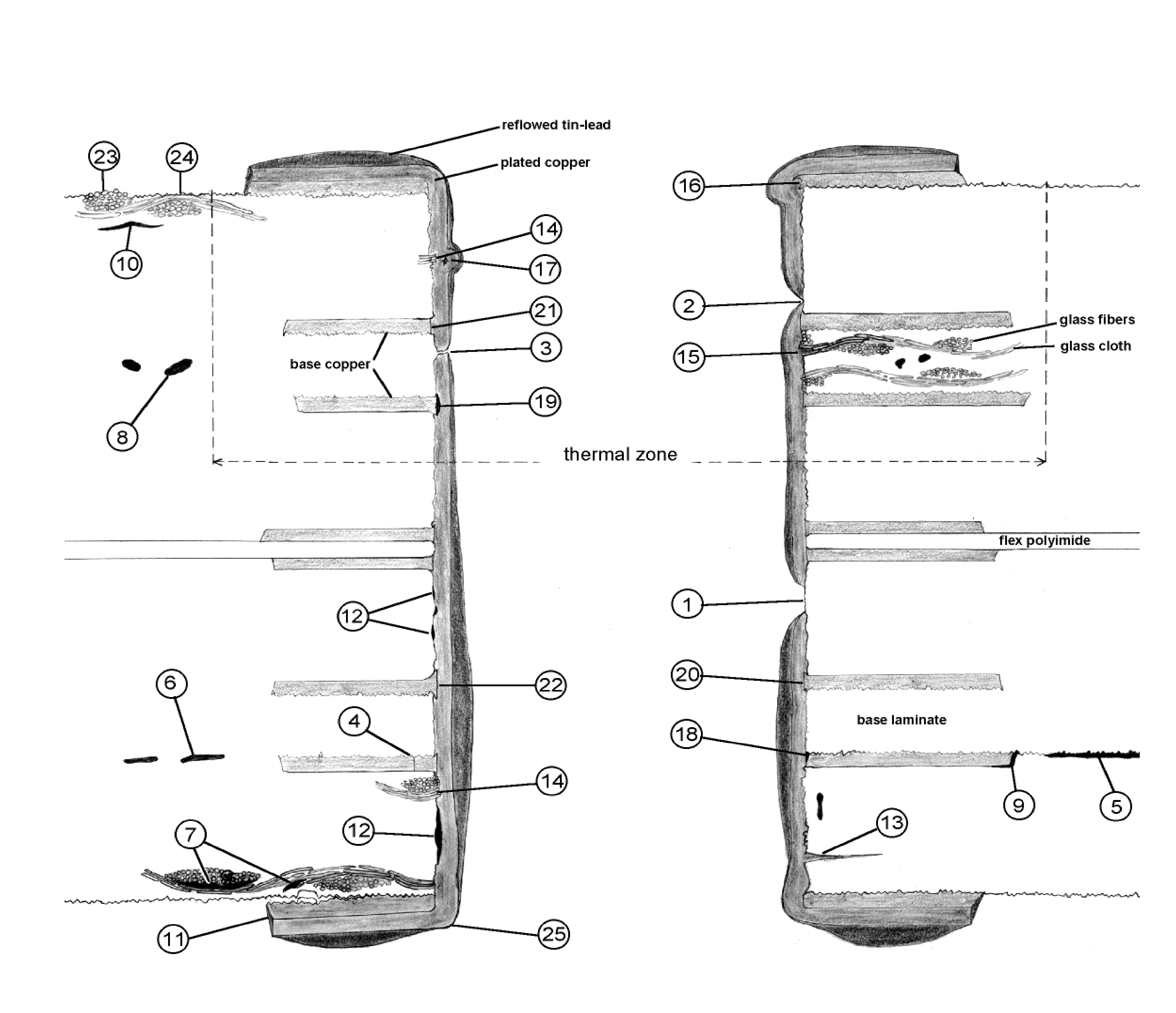 Cross section of a flex-rigid multilayer plated-through hole with typical features and defects
|
1 - plating void
|
14 - glass fibre protrusion
|
|
2 - pinhole
|
15 - rough drilling and wicking (copper)
|
|
3 - plating crack
|
16 - burr
|
|
4 - basic copper crack
|
17 - plating nodule
|
|
5 - delamination
|
18 - smearing
|
|
6 - delamination
|
19 - adhesion defect
|
|
7 - measling
|
20 - positive etch back (inner layer copper
|
|
8 - laminate void (out of thermal zone)
|
imbedded in plated copper)
|
|
9 - resin recession innerlayer
|
21 - negative etch back
|
|
10 - resin crack
|
22 - nailheading
|
|
11 - lifted land
|
23 - weave exposure (fibres visible)
|
|
12 – pull away
|
24 - weave texture (glass cloth shape visible)
|
|
13 - wicking (copper)
|
25 - tin lead thickness 1µ in angles
|
Figure: Example of platedthrough hole microsection
Bibliography
|
ECSS-S-ST-00
|
ECSS system – Description, implementation and general requirements
|
|
IEC 60194 (1999-04)
|
Printed board design, manufacture and assembly — Terms and definitions
|