
Space product assurance
Verification and approval of automatic machine wave soldering
Foreword
This Standard is one of the series of ECSS Standards intended to be applied together for the management, engineering and product assurance in space projects and applications. ECSS is a cooperative effort of the European Space Agency, national space agencies and European industry associations for the purpose of developing and maintaining common standards. Requirements in this Standard are defined in terms of what shall be accomplished, rather than in terms of how to organize and perform the necessary work. This allows existing organizational structures and methods to be applied where they are effective, and for the structures and methods to evolve as necessary without rewriting the standards.
This Standard has been prepared by the ECSS Executive Secretariat endorsed by the document and discipline focal point and approved by the ECSS Technical Authority.
Disclaimer
ECSS does not provide any warranty whatsoever, whether expressed, implied, or statutory, including, but not limited to, any warranty of merchantability or fitness for a particular purpose or any warranty that the contents of the item are error-free. In no respect shall ECSS incur any liability for any damages, including, but not limited to, direct, indirect, special, or consequential damages arising out of, resulting from, or in any way connected to the use of this Standard, whether or not based upon warranty, business agreement, tort, or otherwise; whether or not injury was sustained by persons or property or otherwise; and whether or not loss was sustained from, or arose out of, the results of, the item, or any services that may be provided by ECSS.
Published by: ESA Requirements and Standards Division
ESTEC, ,
2200 AG Noordwijk
The
Copyright: 2010 © by the European Space Agency for the members of ECSS
Change log
|
ECSS-Q-70-07A
|
First issue
|
|
ECSS-Q-ST-70-07B
|
Never issued
|
|
ECSS-Q-ST-70-07C
|
Second issue
|
Introduction
Wave soldering is regarded as a critical process that can find limited application during the assembly of components on to printed circuit boards (PCBs) intended for spacecraft. The preferred procedure is by manual soldering to the requirements of ECSS-Q-ST-70-08. Generally the small number of identically designed circuits does not warrant the setting up of unique machine parameters for each individual layout.
When wave soldering is identified as a suitable alternative to manual soldering for use in the customer’s projects, it can be essential to follow the steps outlined in this document before the final customer’s approval is granted. The sequence of main events is shown in Figure 41. Each step is fully completed and the details recorded, so that a dossier is compiled for each manufacturer’s assembly line. All dossiers are kept updated by the approval authority and serve as a reference for the approval authority’s Project Engineers.
A general qualification is not granted for wave soldering. Wave soldering lines that have been previously verified (see also clause 5.2) can be also approved for use on named projects, but this depends entirely on the specific project requirements. Project process approval is requested, as for all materials and critical processes, by means of ECSS-Q-ST-70.
Scope
This specification defines the basic requirements for the verification and approval of automatic machine wave soldering for use in spacecraft hardware. The process requirements for wave soldering of doublesided and multilayer boards are also defined.
This standard may be tailored for the specific characteristic and constrains of a space project in conformance with ECSS-S-ST-00.
Normative references
The following normative documents contain provisions which, through reference in this text, constitute provisions of this ECSS Standard. For dated references, subsequent amendments to, or revision of any of these publications do not apply. However, parties to agreements based on this ECSS Standard are encouraged to investigate the possibility of applying the more recent editions of the normative documents indicated below. For undated references, the latest edition of the publication referred to applies.
|
ECSS-S-ST-00-01
|
ECSS system - Glossary of terms
|
|
ECSS-Q-ST-10-09
|
Space product assurance – Nonconformance control system
|
|
ECSS-Q-ST-70
|
Space product assurance - Materials, mechanical parts and processes
|
|
ECSS-Q-ST-70-08
|
Space product assurance - Manual soldering of highreliability electrical connections
|
|
ECSS-Q-ST-70-10
|
Space product assurance - Qualification of printed circuit boards
|
|
ECSS-Q-ST-70-28
|
Space product assurance - Repair and modification of printed circuit board assemblies for space use
|
Terms, definitions and abbreviated terms
Terms from other standards
For the purpose of this Standard, the terms and definitions from ECSS-S-ST-00-01 ECSS-Q-ST-70, ECSS-Q-ST-70-08 and ECSS-Q-ST-70-28 apply.
Terms specific to the present standard
approval authority
entity/organization responsible for executing (or sub-contracting) the examination of the technology samples, performing the automatic wave soldering process line-audit, authorizing the implementation of the supplier’s verification programme, and notifying, renewing or withdrawing the approval of the verification
The approval authority is the final customer or the representative nominated by him. For example, for ESA programmes, the final customer is ESA.
component density
number of components per unit board area
ionisable contaminant
process residues that exist as ions and when dissolved, increase electrical conductivity
Examples of such process residues flux are activators, fingerprints, etching and plating salts.
machine oil
liquid compounds formulated for use as oil in wavesoldering equipment
They serve primarily to provide a barrier between the atmosphere and molten solder, thereby reducing the oxidation (drossing) of the solder. Certain oils also reduce the surface tension of molten solder, thereby enhancing the wetting characteristics of the solder.
measling
condition existing in the base laminate of a printed circuit board in the form of discrete white spots or “crosses” below the surface of the base laminate, reflecting a separation of fibres in the glass cloth at the weave intersection
technology samples
samples of wavesolder assembled boards
These samples are provided by the supplier in addition to the application for verification.
wave soldering
process wherein printed circuit boards are brought in contact with a gently overflowing wave of liquid solder which is circulated by a pump in an appropriately designed solder pot reservoir
The prime functions of the molten wave are to serve as a heat source and heat transfer medium and to supply solder to the joint area.
wavesoldering equipment
systems that achieve wave soldering
- 1 A typical wave soldering equipment consist of stations for fluxing, preheating, and soldering by means of a conveyer.
- 2 Cleaning is usually offered as an option. Normally, additional cleaning can be required in order to meet ECSS (or customer specific) cleanliness standards.
Abbreviated terms
For the purpose of this Standard, the abbreviated terms from ECSS-S-ST-00-01 and the following apply:
|
Abbreviation
|
Meaning
|
|
PID
|
process identification document
|
Principles
The sequence of main events for final customer verification and approval of wave soldering process is given in Figure 41.
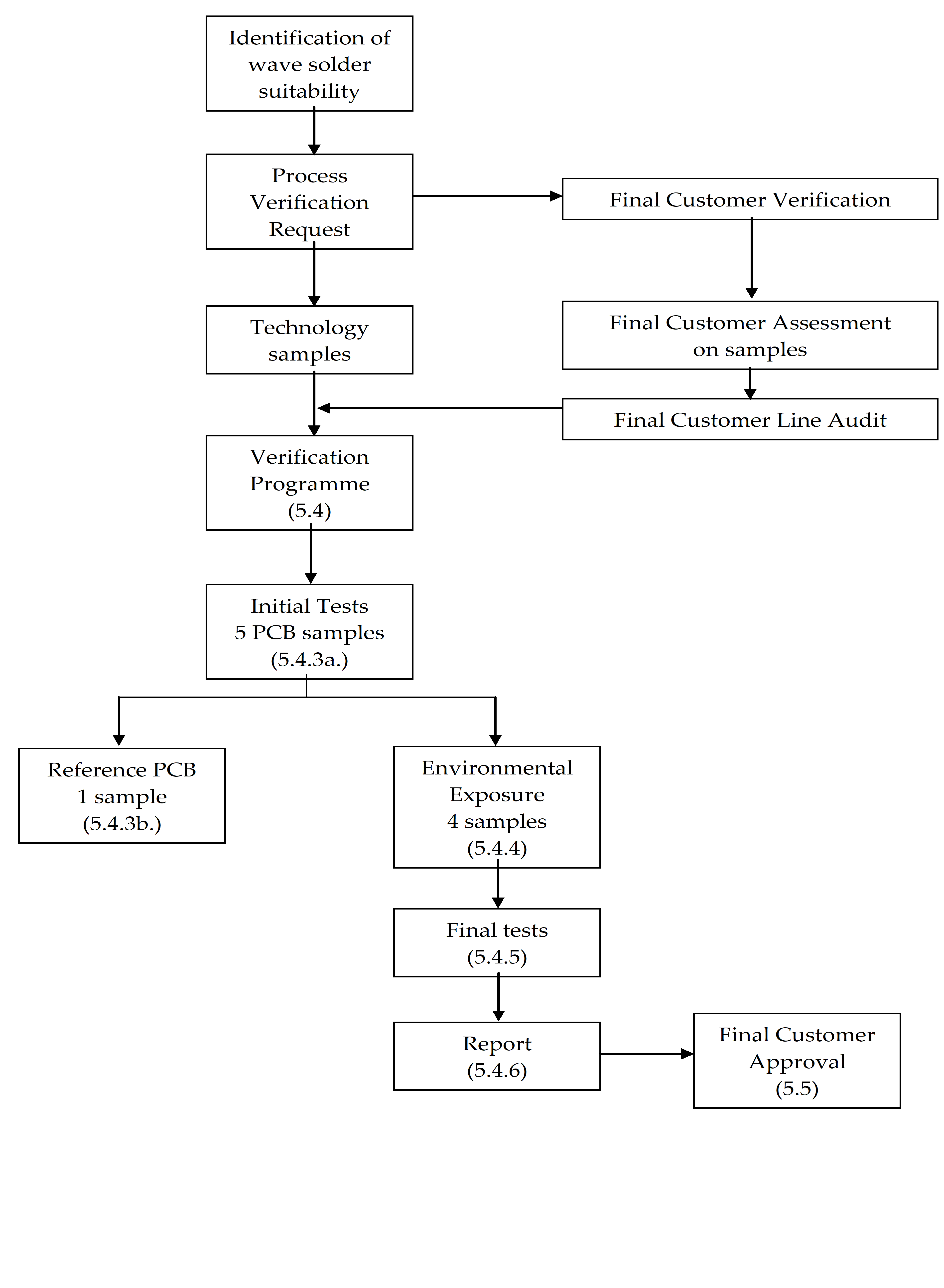 Figure 41: Sequence of main events for final customer verification and approval of wave soldering process
Requirements
General
PCB design constraints
The supplier shall specify to the designers of printed circuit boards intended to be manufactured, the design constraints of using an automatic wave soldering process.
The design constraint specification specified in 5.1.1a shall, at least, include the following statements:
- To avoid solder bridging, orient circuit tracks that are spaced close together in line with the pass direction.
- Avoid large heat sink areas for ground planes and large leads closely connected to massive metal parts.
Rework
For rework of soldered joints, ECSS-Q-ST-70-08 shall apply with a maximum of 5 % rework on each wave soldered circuit
Deficient wavesoldered connections are caused most frequently by the movement of component leads during solidification, the presence of solder alloy within stress relief bends and the entrapment of machine oils and solder fluxes within the solder fillet. Rework of any nature is costly. It involves not only the risk of irreparable lifted pads and measling, but also the possibility of heat damage to sensitive components.
The supplier shall maintain a solder joint discrepancy log in conformance with the DRD in Annex A.
This is an aid to process control, optimization of parameters and repeatability.
Request for verification of the automatic wave soldering process
General
The supplier shall establish a request for verification of the automatic wave soldering process in conformance with Annex B- DRD
The request for verification of the automatic wave soldering process shall be signed by the supplier’s person responsible for space component assembly processes.
The request for verification of the automatic wave soldering process shall be submitted to the approval authority.
Technology samples
In addition to the request for verification of the automatic wave soldering process, the supplier shall provide three technology samples of wavesolder assembled boards whose complexity is typical of that found in spacecraft and which meet spacequality workmanship standards.
The supplier shall perform a cleaning without conformal coating of the samples specified in 5.2.2a.
The technology samples specified in 5.2.2a shall consist of PCBs procured from a spaceapproved manufacturing line, which have been assembled with components according to a documented procedure as specified in clause 5.6.
The supplier shall provide a listing of the manufacturing and assembly procedures specified in 5.2.2c, as part of the line’s Process Identification Document (PID).
Except for the actual machine soldering procedure, the full component assembly requirements of ECSS-Q-ST-70-08 shall apply.
The assembled board shall be free of flux residues and other contaminants.
Examination
The technology samples shall be assessed by the approval authority or by a test house recognized by the approval authority.
The assessment of the technology samples shall include visual and metallographic inspections.
After examination, the technology samples examination report shall be sent to the supplier.
The technology sample examination report is a customer document provided to the supplier and used as input for the customer to decide if the verification programme can be implemented (see 5.4.1a). No DRD is specified for this activity.
Line audit
Provided the technology samples are acceptable, the approval authority shall audit the wavesoldering and related facilities at a time when the equipment is in operation.
The audit shall also include a further onsite review of the documentation listed in clauses B.2.1b and B.2.1h.
Compliance with the process requirements of clause 5.6 shall be evaluated.
The approval authority shall submit to the supplier a copy of the audit report.
The line audit report is a customer document provided to the supplier and is used as input for the customer to decide if the verification programme can be further implemented (see 5.4.1a). No DRD is specified for this activity.
Verification
Planning, management and finance
After the successful completion of the line audit, the supplier shall provide the approval authority with a verification programme and flow chart for approval.
The verification programme shall be performed by the supplier’s quality laboratories under the supervision of a product assurance engineer, or by one or more independent test houses.
Each test house shall obtain the approval authority’s authorisation prior to commencement of the programme.
The supplier shall finance the entire verification programme.
This programme can be monitored by the approval authority at various stages during testing.
Description of samples
The supplier shall provide five PCBs from each production line assembled according to the wavesoldering procedure of clause 5.6.
Each board shall have an identical layout.
This means that they have identical dimensions, number of layers and type of components.
The layout and component density shall be similar to that envisaged for spacecraft circuits.
The variety of component packages mounted on each board shall be restricted to those planned to be used for spacecraft circuits.
There shall be at least three components of each type per board.
It is important to pay particular attention to heat sensitive components.
Only component types utilized during the verification programme shall be regarded as process approved.
Owing to the high cost of some components, the approval authority can agree to the use of nonfunctional, or commercialquality components.
In case of using nonfunctional, or commercialquality components, they shall be of the same lead material and finish (i.e. solderability) as the hirel components required for flight.
Initial tests
The supplier shall perform the following initial tests on each of the five assembled PCBs:
- Visual inspection in conformance with the requirements of ECSS-Q-ST-70-08;
- Cleanliness test in conformance with clause 11.3 of ECSS-Q-ST-70-08;
- Warp (bow) and twist of circuit board in conformance with the requirements of ECSS-Q-ST-70-10, with the limits given in Table 51. Table 51: Limits for warp and twist
|
Board thickness (mm)
|
l≤0,7
|
0,8-1,1
|
1,2-1,51
|
≥1,61
|
|
Warp and twist (%)
|
2,6
|
1,8
|
1,41
|
1,11
|
- For multilayer boards, measurement of electrical continuity at least 25 % of all holes with at least one internal connection per hole in conformance with the requirements of ECSS-Q-ST-70-10.
Double-sided PCB are not considered multilayer boards.
The supplier shall keep one printed circuit board for reference.
This board is used as a reference to compare the results of the pull test specified in 5.4.5a.7 to 5.4.5a.11.
Environmental exposure
The four test samples not kept for reference after the initial tests specified in 5.4.3 shall be temperature cycled in air, 200 cycles from -55 °C to +100 °C, at an average heating or cooling rate not exceeding 10 °C/min.
The sample dwell time shall be a minimum of 15 minutes at each of the temperature extremes.
In case the assemblies deviate from the design requirements and workmanship standards of ECSS-Q-ST-70-08, the assembled PCBs shall be vibration tested.
Final tests
Following completion of the temperature cycles specified in 5.4.4, the supplier shall perform the following procedure:
- inspect visually each sample in accordance with the requirements of ECSS-Q-ST-70-08;
- perform electrical continuity measurements for multilayer boards which are monitored throughout a further 10 thermal cycles;
- classify multilayer boards with positive changes greater than 5 % as failed;
- select those components for microsectioning having, from visual inspection results, the worst solder fillet aspect;
- perform microsectioning on at least two components, of each available type, so as to dissect their component leads;
- classify components with evidence of propagating cracks in the solder joint vicinity as failed, and verify that there are no defects in the board;
- cut and pull-test the leads of at least two components at a constant strain rate;
- perform pull-testing in a direction perpendicular (+5°) to the board surface;
- record fracture loads and positions;
- compare the results with the values obtained for identical components on the reference board;
- classify components with a 25 % reduction of mechanical strength after environmental testing as failed.
Final verification report
After completion of the verification programme, the supplier shall submit to the approval authority, the final automatic wave soldering process verification report in conformance with the DRD in Annex C.
Approval
Notification
On successful completion of the verification programme and the submittal of the report to the approval authority, this approval authority shall send a letter to the supplier confirming that the verification programme has been approved.
When there are no changes to the Process Identification Document (PID) the period of validity is indefinite and takes effect from the date on which the successful verification programme ended.
Renewal of approval
A new verification test programme shall be carried out whenever a change to the PID is proposed.
Withdrawal of approval
The approval of any wavesoldering line shall be withdrawn by the approval authority in any of the following cases:
- the supplier experiences rework activities of more than 5 %,
- any of the materials, permitted component types or manufacturing processes have been changed without prior authorization (i.e. changes to the PID),
- modifications related to B.2.1b as given in the Annex C –DRD. have taken place, without an approval before implementation,
- the customer or his intermediate suppliers have experienced delays in delivery or manufacturing defects directly attributable to the wavesoldering process.
- 1 Renewed approval can be granted following a review of the discrepancy(ies).
- 2 A repeat, or partial repeat of the verification programme can be considered necessary.
Approval for future project
The supplier shall make requests for future project approval, through submission of the project declared process list (DPL) in conformance with the DRD in Annex C of ECSS-Q-ST-70.
This is the same process as for all critical processes.
Process requirements for wave soldering of printed circuit boards
For all materials and processes utilized in soldering and cleaning operations, ECSS-Q-ST-70-08 and ECSS-Q-ST-70-10 shall apply.
Nonactivated rosin fluxes shall be used.
Refer to ECSS-Q-ST-70-08 for approved flux products.
All fluxes shall be adjusted frequently.
- 1 E.g. specific gravity.
- 2 This is to avoid variations from the optimum.
When mildly activated fluxes are permitted and used, they shall be changed frequently.
This ensures a constant and adequate level of activation.
All fluxes, machine oils and ionisable contaminants on the assembly shall be removed within one hour of the wavesoldering operation.
The soldering area and machines shall be kept clean and orderly.
Electrostaticdischarge problems shall be avoided as defined in ECSS-Q-ST-70-08.
The conveyer shall be grounded.
Toxic or volatile vapours shall be exhausted.
Lighting facilities and component lead preparations shall be maintained as defined in ECSS-Q-ST-70-08.
For any deviations, the supplier shall obtain the approval of the approval authority before implementation.
Dross (oxides) from the solder bath shall be removed periodically to ensure that dross does not mix with the liquid solder..
Automatic or manual methods are acceptable, provided that the dross does not come in contact with the PCB assembly during any portion of the soldering process.
Dross removal materials that melt, dissolve or alloy with the liquid solder and flux shall not be used.
The PCB assemblies shall:
- be heated uniformly, and
- have, by means of the soldering equipment, the capacity to maintain the temperature during repetitive solder operations with a maximum variation of +5 °C of the normal soldering temperature.
The supplier shall maintain all operating procedures which describe the soldering process and its associated equipment in conformance with the PID produced in accordance with DRD in Annex E.
For the soldering machine, the supplier shall provide these procedures, as a minimum for given PCB assembly layouts, in conformance with the DRD in Annex E.
Evidences shall be provided that: - the assembled board does not become contaminated before being loaded on the carrier.
- the conveyer speed does not vary by more than ±5 %. The following wave soldering machine parameters shall be controlled:
- the preheat temperature to avoid damage to the PCB and the component packages.
- the solder temperature so that the solder in the wave making contact with the board is 235 °C to 275 °C.
See also step 5.6n.
- the height of the solder wave to a constant preselected value across the width of the wave.
The above three parameters are recorded in Annex A-DRD
The supplier shall maintain a machinesoldering logbook in conformance with Annex D-DRD
The supplier shall apply cleanliness checks in conformance with the requirements of ECSS-Q-ST-70-08 at established intervals, to preestablished resistivity limits.
These intervals are based on the number and size of boards cleaned as well as time.
For all machinesoldered assemblies, the supplier shall perform inspection in conformance with the inspection criteria detailed in ECSS-Q-ST-70-08.
Evidences shall be provided that:
- warp and twist of the board do not exceed the limits specified in Table 51.
- any reworked boards:
- Have been reworked by hand soldering.
- The maximum 5 % of the solder connections requirement is not exceeded.
- Are further cleaned and cleanliness tested.
- Meet all the visual inspection and cleanliness requirements of this clause 5.6.
- the leads of spacecraft components which are designed for lapsoldering onto specially designed pads are not bent and subjected to wave soldering and thus are assembled manually to the PCB in a subsequent operation and according to the requirements of ECSS-Q-ST-70-08.
ANNEX(normative)Solder joint discrepancy log – DRD
DRD identification
Requirement identification and source document
This DRD is called from ECSS-Q-ST-70-07, requirement 5.1.2b.
Purpose and objective
The purpose of this document is to maintain a solder joint services history file for each automatic wave soldered PCB assembly in order to record problems and non conformance reports and to provide inputs for:
Automatic wave soldering process control,
Optimization of parameters,
Repeatability.
Expected response
Scope and content
The solder joint discrepancy log shall contain, for each PCB assembly that has been wave soldered with the soldering machine, the measurements of the following process control parameters:
- the preheat temperature,
- the conveyer speed,
- the solder temperature and,
- the height of the wave. The solder joint discrepancy log shall list the discrepancies from the initial customer’s requirements identified for each PCB assembly for a given set of control parameters measurements.
Special remarks
An example of solder joint discrepancy log is given in Figure A-1
|
Part identification Wave soldering parametersAssembly: __________ PCB P/N: __________ Preheat temp: ________ Solder temp: ________ Conveyer Speed: ________ Wave height: _________
| |||||||||||||||||||
|
Description
|
Insufficient
|
Excess
|
Miscellaneous
|
|
|||||||||||||||
|
MLB No. of thru holes: ______ No. of layers: ______Ground plane estimated area: Topside: ______% Botside: ______%
|
T: component side; B: bottom side
|
Lead poor wetting
|
Pad poor wetting
|
Large voids
|
Small bottomless voids
|
Insufficient solder flow-thru
|
Depressed solder
|
Bridging
|
Icicling
|
Accumulations
|
Excess solder (lead obscured)
|
Stress-relief bends filled
|
Raised component
|
|
|||||
|
Acceptable rework level: ___% total
|
Date
|
Inspector
|
Insptn. S/N
|
Other solder discrepancies (specify)
|
Subtotals
|
% for rework
| |||||||||||||
|
Inspector’s observations:
|
|
|
|
T
|
|
|
|
|
|
|
|
|
|
|
|
|
|
|
|
|
B
|
|
|
|
|
|
|
|
|
|
|
|
|
|
||||||
|
|
|
|
T
|
|
|
|
|
|
|
|
|
|
|
|
|
|
|
|
|
|
B
|
|
|
|
|
|
|
|
|
|
|
|
|
|
||||||
|
|
|
|
T
|
|
|
|
|
|
|
|
|
|
|
|
|
|
|
|
|
|
B
|
|
|
|
|
|
|
|
|
|
|
|
|
|
||||||
|
|
|
|
T
|
|
|
|
|
|
|
|
|
|
|
|
|
|
|
|
|
|
B
|
|
|
|
|
|
|
|
|
|
|
|
|
|
||||||
|
|
|
|
T
|
|
|
|
|
|
|
|
|
|
|
|
|
|
|
|
|
|
B
|
|
|
|
|
|
|
|
|
|
|
|
|
|
||||||
|
|
|
|
T
|
|
|
|
|
|
|
|
|
|
|
|
|
|
|
|
|
|
B
|
|
|
|
|
|
|
|
|
|
|
|
|
|
||||||
|
Totals:
| |||||||||||||||||||
Figure: Example of a solder joint discrepancy log
ANNEX(normative)Request for verification of the automatic wave soldering process - DRD
DRD identification
Requirement identification and source document
This DRD is called from ECSS-Q-ST-70-07, requirement 5.2.1a.
Purpose and objective
The purpose of the request for verification of the automatic wave soldering process is: to:
Allow a supplier to initiate formally the verification of its automatic wave soldering process.
Supply the approval authority with all the necessary pre-requisites (documentation, technology samples) prior to authorisation of the implementation of the verification programme.
Expected response
Scope and content
The request for verification of the automatic wave soldering process shall contain a brief description of the facility, details of past experience and the name of the spacecraft project concerned.
The request for verification of the automatic wave soldering process shall include or refer to the following information:
- Company organization chart and responsibilities related to wavesoldering production and control personnel.
This includes names and functions of all key personnel involved.
- List of materials used for wave soldering including types and names of supplier.
Materials such as solder, flux, solvents, PCBs and equipment.
- Production flow chart detailing optimized machine parameters, and quality assurance inspection points.
The request for verification of the automatic wave soldering process shall include or refer to the list of process specifications, including reference numbers of relevant in-house documents.
The request for verification of the automatic wave soldering process shall include the reference to the applicable general process requirements if different of the requirements already listed in clause 5.6.
The request for verification of the automatic wave soldering process shall include or refer to the detailed report concerning optimization of wavesoldering process parameters.
The request for verification of the automatic wave soldering process shall outline company test capabilities.
Test capabilities like thermal cycling chambers, metallography, chemical analysis, failure analysis.
The request for verification of the automatic wave soldering process shall include the documentation of the technology samples.
As part of the technology sample documentation, the following information shall be provided:
- type of components,
- list of used materials,
- description of processes including machine parameters,
- summary of cleanliness test results in conformance with clause 11 of ECSS-Q-ST-70-08 or equivalent method.
Special remarks
None.
ANNEX(normative) Automatic wave soldering process verification report – DRD
DRD identification
Requirement identification and source document
This DRD is called from ECSS-Q-ST-70-07, requirement 5.4.6a.
Purpose and objective
The purpose of the report is to summarize all the verification test specifications, procedures and test results which are relevant for the approval of the automatic wave soldering process verification.
Expected response
Scope and content
The verification report shall include the verification of the samples, covering for each component type:
- component lead material and finish;
- lead diametertohole diameter ratio. The verification report shall contain for the 5 assembled PCBs specified in 5.4.2 (including the one used for reference), the initial test specifications, procedures and test results as defined in the verification programme, including:
- Visual inspection report established in conformance with the requirements of ECSS-Q-ST-70-08;
- Summary of cleanliness test results in conformance with clause 11.3 of ECSS-Q-ST-70-08 or equivalent method;
- Tests results concerning the warp (bow) and twist of circuit board in conformance with the requirements of ECSS-Q-ST-70-10;
- Electrical continuity test specification, procedure and reports (for multilayer boards).
The verification report shall contain the full results of all tests performed to clauses 5.4.3 and 5.4.5.
The report shall contain photographic evidences of the tested assembled boards where possible.
The automatic wave soldering process verification report shall contain a list of findings and recommendations in order to optimize the automatic wave soldering process specifications and control parameters for a given assembled PCB.
Except for research and development activities, the automatic wave soldering process verification report shall include the list of potential nonconformances or deviations to be handled in conformance with ECSS-Q-ST-10-09.
Special remarks
None
ANNEX(normative)Machine-soldering logbook – DRD
DRD identification
Requirement identification and source document
This DRD is called from ECSS-Q-ST-70-07, requirement 5.6s.
Purpose and objective
The purpose of the logbook is to collect and summarize all the necessary machine parameters in order to optimize the soldering process, independently of the PCB manufacturing assembly process to be carried out.
Expected response
Scope and content
The machine soldering logbook shall contain the following control parameters to be measured
- Preheat temperature,
- The conveyer speed,
- The solder temperature,
- The height of the wave.
The machine soldering logbook shall contain the results of the solder-bath analysis.
The machine soldering logbook shall contain the results of the cleanliness test.
Special remarks
None.
ANNEX(normative)Wave soldering process identification document (PID) – DRD
DRD identification
Requirement identification and source document
This DRD is called from ECSS-Q-ST-70-07, requirements 5.6o and 5.6p.
Purpose and objective
The purpose of the document is to summarize, as a minimum for given PCB assembly layouts, the definitions of the soldering machine and related processes.
Expected response
Scope and content
The PID shall list all the wave soldering process and control specifications and procedures with number, issue number and date for the full automatic wave soldering process, for different given PCB assembly layouts, including the following items:
- All wave soldered PCB assembly specifications and procedures.
- The machine soldering production flow chart detailing optimized machine parameters, and quality assurance inspection points.
- All operating procedures describing the step by step operations of the soldering process and its associated equipments.
Special remarks
None.
Bibliography
|
ECSS-S-ST-00
|
ECSS system – Description, implementation and general requirements
|