
Space product assurance
Qualification and procurement of printed circuit boards
Foreword
This Standard is one of the series of ECSS Standards intended to be applied together for the management, engineering and product assurance in space projects and applications. ECSS is a cooperative effort of the European Space Agency, national space agencies and European industry associations for the purpose of developing and maintaining common standards. Requirements in this Standard are defined in terms of what shall be accomplished, rather than in terms of how to organize and perform the necessary work. This allows existing organizational structures and methods to be applied where they are effective, and for the structures and methods to evolve as necessary without rewriting the standards.
This Standard has been prepared by the ECSS Executive Secretariat, endorsed by the Document and Discipline Focal Points, and approved by the ECSS Technical Authority.
Disclaimer
ECSS does not provide any warranty whatsoever, whether expressed, implied, or statutory, including, but not limited to, any warranty of merchantability or fitness for a particular purpose or any warranty that the contents of the item are error-free. In no respect shall ECSS incur any liability for any damages, including, but not limited to, direct, indirect, special, or consequential damages arising out of, resulting from, or in any way connected to the use of this Standard, whether or not based upon warranty, business agreement, tort, or otherwise; whether or not injury was sustained by persons or property or otherwise; and whether or not loss was sustained from, or arose out of, the results of, the item, or any services that may be provided by ECSS.
Published by: ESA Requirements and Standards Division
ESTEC, P.O. Box 299,
2200 AG Noordwijk
The Netherlands
Copyright: 2019 © by the European Space Agency for the members of ECSS
Change log
|
ECSS-Q-ST-70-60C
|
First issue
|
|
ECSS-Q-ST-70-60C Corrigendum 1
|
First issue, Corrigendum 1
|
|
History of superseded versions
| |
|
ECSS-Q-70-10A
|
First issue
|
|
ECSS-Q-70-10B
|
Never issued
|
|
ECSS-Q-ST-70-10C
|
Second issue
|
Introduction
PCBs are used for the mounting of electronic components to produce PCB assemblies that perform electrical functions. The PCBs are subjected to thermo-mechanical stress during assembly such as soldering of components, rework and repair under normal terrestrial conditions. In addition, the assembled PCBs are exposed to the launch and space environment. The reliability of the circuit depends on the robustness of the manufacturing processes, for which this standard specifies requirements. PCB technology needs detailed inspections to verify its reliability, which is specified for the qualification and procurement phases of the PCB technology.
Scope
This standard specifies the requirements for the PCB manufacturer, the procurement authority and the qualification authority for qualification and procurement of PCB technology.
ECSS-Q-ST-70-60 is applicable for all types of PCBs, including sequential, rigid and flexible PCBs, sculptured flex, HDI and RF PCBs.
This standard can be made applicable for other products combining mechanical and electrical functionality using additive or reductive manufacturing processes, as used in PCB manufacturing. Examples of such products are slip- rings, bus bars and flexible flat cables.
This standard may be tailored for the specific characteristics and constraints of a space project in conformance with ECSS-S-ST-00.
Normative references
The following normative documents contain provisions which, through reference in this text, constitute provisions of this ECSS Standard. For dated references, subsequent amendments to, or revision of any of these publications do not apply. However, parties to agreements based on this ECSS Standard are encouraged to investigate the possibility of applying the more recent editions of the normative documents indicated below. For undated references, the latest edition of the publication referred to applies.
|
ECSS-S-ST-00-01
|
ECSS system — Glossary of terms
| |
|
ECSS-Q-ST-10-09
|
Space product assurance — Nonconformance control system
| |
|
ECSS-Q-ST-20
|
Space product assurance — Quality assurance
| |
|
ECSS-Q-ST-70
|
Space product assurance — Material, mechanical parts and processes
| |
|
ECSS-Q-ST-70-02
|
Space product assurance — Thermal vacuum outgassing test for the screening of space materials
| |
|
ECSS-Q-ST-70-08
|
Space product assurance — Manual soldering of highreliability electrical connections
| |
|
ECSS-Q-ST-70-12
|
Space product assurance — Design rules for printed circuit boards
| |
|
ECSS-Q-ST-70-21
|
Space product assurance — Flammability testing for the screening of space materials
| |
|
ECSS-Q-ST-70-22
|
Space product assurance — Control of limited shelflife materials
| |
|
ECSS-Q-ST-70-29
|
Space product assurance — Determination of offgassing products from materials and assembled articles to be used in a manned space vehicle crew compartment
| |
|
ECSS-Q-ST-70-38
|
Space product assurance —High reliability soldering for surface mount and mixed technology printed circuit boards
| |
|
EN 9100:2016
|
Quality management systems – Requirements for aviation, space and defense organisations
| |
|
IEC 60326-2-am 1 (1992-06)
|
Printed boards. Part 2: Test methods
| |
|
IEC 60194 (1999-04)
|
Printed board design, manufacture and assembly — Terms and definitions
| |
|
IPC-A-600J (2016)
|
Acceptability of Printed Boards
|
|
|
IPC-T-50M (2015)
|
Terms and definitions for interconnecting and packaging electronic circuits
| |
|
IPC-TM-650
|
Test methods manual
| |
|
IPC-1710A (2004)
|
OEM Standard for Printed Board Manufacturers' Qualification Profile
| |
|
IPC-4101E (2017)
|
Specification for base materials for rigid and multilayer printed boards
| |
|
IPC-4103A-WAM1 (2014)
|
Specification for Base Materials for High Speed/
| |
|
IPC-4203A (2013)
|
Adhesive Coated Dielectric Films for Use as Cover Sheets for Flexible Printed Circuitry and Flexible Adhesive Bonding Films
| |
|
IPC-4204A-WAM1 (2014)
|
Flexible Metal-Clad Dielectrics for Use in Fabrication of Flexible Printed Circuitry
| |
|
IPC-6012D (2015)
|
Qualification and performance specification for rigid printed boards
| |
|
IPC-6012DS (2015)
|
Space and military avionics applications addendum to IPC-6012D
| |
|
IPC-6013D (2017)
|
Qualification and Performance Specification for Flexible Printed Boards
| |
|
IPC-6018C (2016)
|
Qualification and Performance Specification for High Frequency (Microwave) Printed Boards
| |
|
IPC-6018CS (2016)
|
Space and Military Avionics Applications Addendum to IPC-6018C
| |
|
ISO 9001:2015
|
Quality management systems - Requirements
| |
|
ISO-14644-1 (2015)
|
Cleanrooms and associated controlled environments - Part 1: Classification of air cleanliness by particle concentration
|
Terms, definitions and abbreviated terms
Terms from other standards
For the purpose of this Standard, the terms and definitions from ECSS-S-ST-00-01 apply, and in particular the following terms:
customer
supplier
See clause 4.2 for a description of roles of customer and supplier.
For the purpose of this Standard, the terms and definitions from ECSS-Q-ST-70-12 apply, and in particular the following terms:
annular ring
area array device (AAD)
aspect ratio
basic copper
blind via
bond-ply
build-up
buried via
conductor
FR4
hole wall pull away
heat sink
high density interconnect (HDI)
interlayer
intralayer
laminate
microvia
no-flow prepreg
non-functional pad
non-pated hole
normal pitch
panel
plated through-hole (PTH)
prepreg
printed circuit board (PCB)
resin starvation
serialization
spacing
stack
track
via
X,Y direction
Z direction
Terms specific to the present standard
automated optical inspection (AOI)
inspection method using an automated equipment to verify the pattern on an etched layer
back-drilled via
type of via with part of its metallisation removed on one side by depth controlled mechanical drilling with a larger diameter drill
batch
group of PCBs and coupons that are covered by the same CoC and the same traveller
- 1 A batch is processed approximately at the same time. See 6.8a.
- 2 The terms “lot” and “work order” are synonymous.
blind-via-in-pad
type of via directly underneath a SMT pad
blister
delamination in the form of a localized swelling and separation between any of the layers of a laminated base material, or between base material and conductive foil or protective coating
[IPC-T-50M]
cap lift
separation between resin in blind via and copper cap plating on surface
Cap lift can be shown as bulging and as thin line separation, as shown in Table 1018.
contamination
<CONTEXT: Qualification and procurement of PCBs>
foreign material embedded in dielectric material
-
1 Synonyms are: FOD, inclusion (see definition 3.2.20), foreign material, debris, pollution.
-
2 Contamination can be organic, metallic, particulate or fibres.
coupon
small piece of test circuitry that is used for quality conformance evaluation by specific tests and inspection -
1 The coupon is manufactured as part of a panel and at the final manufacturing stage it is separated from it. The coupon is thus associated with the PCBs within the panel, with which it was simultaneously manufactured.
-
2 The term ‘coupon’ refers to a generic pattern, whereas the term ‘IST coupon’ refers to the specific IST pattern.
[adapted from IPC-T-50M]
coverlay
thin dielectric material used to encapsulate circuitry, most commonly for flexible circuit applications
The terms ‘cover layer’ and ‘cover material’ are synonymous.
crazing
condition that occurs in reinforced laminate base material whereby glass fibre bundles are separated from the resin not limited to the weave intersections
- 1 This condition manifests itself in the form of connected white spots or crosses that are below the surface of the base material. It is usually related to thermally or mechanically induced stress. Crazing is a more severe defect than measling. Delamination is a further worsening of crazing.
- 2 See also “measling”.
delamination
separation between plies within a base material, between base material and a conductive foil, or any other planar separation with a PCB
See also ‘blister’, which is a local delamination.
[IPC-T-50M]
destructive physical analysis (DPA)
analysis method using sampling, potting, grinding, polishing and inspection which, thus, destroys the test vehicle
The term ‘microsectioning’ is approximately synonymous.
dewetting
condition that results when molten solder coats a surface and then recedes to leave irregularlyshaped mounds of solder that are separated by areas that are covered with a thin film of solder and with the base metal not exposed
[IPC-T-50M]
dross
oxide and other contaminants that form on the surface of molten solder
[IPC-T-50M]
etchback
distance from resin of hole wall to innerlayer foil
fine pitch
spacing of tracks or pads that is more dense than for normal pitch
Pitch is specified in clause 7.4 of ECSS-Q-ST-70-12.
flexible
PCB technology that uses only flexible layers in its build up
The term ’flex’ is synonymous.
glass compression
deformed glass fibre bundles of prepreg causing absence of resin between glass and copper due to profiled copper pattern
See also ‘resin starvation’.
haloing
mechanicallyinduced fracturing or delamination, on or below the surface of a base material, that is usually exhibited by a light area around holes or other machined features
[IPC-T-50M]
inclusion
foreign particle, metallic or nonmetallic, that can be entrapped in an insulating material, conductive layer, plating, base material or solder connection
[IPC-T-50M]
interconnect defect (ICD)
separation at the interface between internal layer and through-hole plating
- 1 The term ‘innerlayer separation’ is synonymous.
- 2 See ‘smear’ for additional explanation.
[IPC-6012D]
interconnect stress test (IST)
test method using a specific IST coupon and a specific IST equipment
IST coupon
specific coupon for IST
The term ‘coupon’ refers to a generic pattern, whereas the term ‘IST coupon’ refers to the specific IST pattern.
key personnel
personnel with specialist knowledge responsible for defined production or product assurance areas
lay-out
design of the conductive pattern on a layer
measling
condition that occurs in laminated base material whereby glass fibre bundles are separated from the resin limited to the weave intersection
- 1 This condition manifests itself in the form of discrete white spots or “crosses” that are below the surface of the base material. It is usually related to thermallyinduced stress or humidity.
- 2 See also “crazing”, which is a further worsening of measling.
[IPC-T-50M]
metal core
layer or local insert of thick metal embedded inside the PCB usually used as a heat sink, grounding layer or restriction of thermal expansion
milling
mechanical method that removes a portion of the material outlining a PCB using a cutting bit
See also ‘routing’.
multilayer
PCB technology that uses lamination of several copper layers and plated holes for interconnection
PCBs that are not multilayer, are double-sided or single-sided PCBs. See also “sequential”.
plated hole
hole that is used as an interlayer connection
Types of plated holes are PTH and vias.
PCB manufacturer
entity that manufactures the PCB
The PCB manufacturer is supplier to the procurement authority.
PCB technology
category of manufacturing processes, materials and design for PCBs
Examples of PCB technology are:
- Polyimide sequential rigid
- Polyimide sequential rigid/flex
- Epoxy sequential rigid
- Epoxy non-sequential rigid/flex
- HDI with microvias
- RF
- Flexible and sculptured flex
plugged via
via type that is cap plated and filled with resin in a specific via filling process
Blind vias can be resin-filled using resin from the prepreg during sequential lamination. Plugged vias use a resin that does not originate from the prepreg and the filling process does not occur during lamination.
procurement authority
entity that procures the PCB
- 1 The procurement authority is customer of the PCB manufacturer.
- 2 The procurement authority can be supplier to the prime contractor.
qualification authority
entity that qualifies the PCB technology and PCB manufacturer
radio frequency (RF)
electronic functionality that requires specific design precautions on dielectric materials and copper pattern to maintain time dependant signal integrity
- 1 The term ‘high speed’ is synonymous.
- 2 The term ‘RF PCB’ identifies the PCB technology.
rigid
PCB technology that uses only rigid layers in its build-up
rigid/flex
PCB technology that uses a combination of rigid and flexible layers in its build-up
routing
the lay-out and connection of conductors between plated-holes and pads
The term ‘routing’ is also used for ‘milling’. This second meaning is not used in ECSS-Q-ST-70-60 to avoid confusion.
scratch
narrow furrow or grove in a surface
It is usually shallow and caused by the marking or rasping of the surface with a pointed or sharp object.
[IEC 60194 (1999-04)]
sculptured flex
flexible PCB technology that uses profiled copper tracks
Aviflex is a commercial identification of sculptured flex.
sequential
PCB technology that uses more than one lamination or drilling step
The term ‘sequential’ also implies that the PCB is of type ‘multilayer’. The opposite is ‘non-sequential’.
sequential via
via type that interconnects layers within the same plating sequence
Examples of sequential vias are blind vias and buried vias.
skip plating
local missing deposition of plating
Skip plating can occur on electroless copper plating on glass in the hole wall. Skip plating can also occur on surface finish.
smear
base material resin that covers the interface between the exposed edge of an innerlayer pad and through-hole plating
- 1 The resin transfer is usually caused by the drilling operation and removed during the desmear process. The term ‘resin smear’ or ‘smearing’ are synonymous.
- 2 The aspect of smear can be mistaken for interconnect defect, or vice versa. Smear is the presence of resin, whereas interconnect defect is an adhesive separation of copper plating.
[adapted from IPC-T-50M]
test pattern
part of the PCB or coupon that refers to the copper pattern for a specific test
[adapted from IPC-T-50M]
through-going via
type of via that is drilled through the entire thickness of the PCB
traveller
documentation kept with the batch during the manufacturing processes in which the order of specific processes are recorded
treatment side of foil
the side of copper foil that is submitted to a surface treatment process by the materials supplier or by the PCB manufacturer
The material supplier treatment side of copper foil on laminate is typically rougher. See Figure 31.
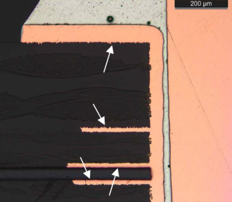 Figure 31: Example of material supplier treatment side of foil (white arrows) and PCB manufacturer treatment side of foil (opposite side)
waiver request
written agreement between PCB manufacturer and procurement authority to deliver PCBs with a nonconformance to a requirement from a specification
- 1 The following terms are synonymous: “request for concession”, “demande de derogation”, “request for waiver”, “request for deviation”.
- 2 In space projects the terms RFW and RFD have specific meaning as specified in ECSS-Q-ST-70. This specific meaning does not strictly apply in the context of PCB procurement.
weave exposure
a base material surface condition in which unbroken fibres of woven glass are not completely covered by resin
See also ‘weave texture’.
[IPC-T-50M]
weave texture
a surface condition of base material in which a weave pattern of cloth is apparent although the unbroken fibres of woven cloth are completely covered by resin.
See also ‘weave exposure’.
[IPC-T-50M]
wicking
infiltration of copper plating into the dielectric of the hole wall
The terms “copper infiltration” and “copper ingress” are synonymous.
work instruction
quality document that describes the technical details about processes, material usage, inspection and acceptance criteria
- 1 The terms ‘manufacturing procedure’ or ‘control procedure’ or ‘process instruction’ are synonymous.
- 2 Work instructions can include process flow charts, production documents (e.g. manufacturing plans, travelers, routers, work orders, process cards) and inspection documents.
Abbreviated terms
For the purpose of this Standard, the abbreviated terms from ECSS-S-ST-00-01 and the following apply:
|
Abbreviation
|
Meaning
|
|
AAD
|
area array device
|
|
AC
|
alternating current
|
|
AOI
|
automated optical inspection
|
|
AR
|
as received
|
|
CDR
|
critical design review
|
|
CIC
|
copper-invar-copper
|
|
CoC
|
certificate of conformance
|
|
CTE
|
coefficient of thermal expansion
|
|
Cu
|
copper (element)
|
|
CVCM
|
collected volatile condensable material
|
|
DC
|
direct current
|
|
DML
|
declared materials list
|
|
DPA
|
destructive physical analysis
|
|
DR
|
design review
|
|
DRB
|
delivery review board
|
|
DRD
|
document requirements definition
|
|
DSC
|
differential scanning calorimetry
|
|
DWV
|
dielectric withstanding voltage
|
|
EBB
|
elegant breadboard
|
|
ECM
|
electrochemical migration
|
|
EM
|
engineering model
|
|
EOL
|
end of life
|
|
EQM
|
engineering qualification model
|
|
FAI
|
first article inspection
|
|
FCSI
|
final customer source inspection
|
|
FM
|
flight model
|
|
FOD
|
foreign object debris
|
|
FR4
|
type of epoxy resin for PCBs
|
|
FS
|
flight spare
|
|
HDI
|
high density interconnect
|
|
ICD
|
interconnect defect
|
|
IMC
|
intermetallic compound
|
|
IPA
|
isopropanol
|
|
IPC
|
association connecting electronic industries
|
|
IST
|
interconnect stress test
|
|
KPI
|
key performance indicator
|
|
max
|
maximum
|
|
min
|
minimum
|
|
MIP
|
mandatory inspection point
|
|
MPCB
|
material and processes control board
|
|
MRR
|
manufacturing readiness review
|
|
MTO
|
metal turnover
|
|
n. a.
|
not applicable
|
|
NCR
|
nonconformance report
|
|
NRB
|
nonconformance review board
|
|
OTD
|
on time delivery
|
|
PCB
|
printed circuit board
|
|
PCN
|
process change notice
|
|
PDR
|
preliminary design review
|
|
PFM
|
proto flight model
|
|
PID
|
process identification document
|
|
PTH
|
platedthrough hole
|
|
PTFE
|
polytetrafluoroethylene
|
|
QA
|
quality assurance
|
|
QM
|
qualification model
|
|
QML
|
qualified manufacturers list
|
|
QPL
|
qualified product list
|
|
r.m.s.
|
rootmeansquare
|
|
R&D
|
research and development
|
|
Ref
|
reference (for tables in clause 10)
|
|
RF
|
radio frequency
|
|
RFA
|
request for approval
|
|
RML
|
residual mass loss
|
|
RW
|
rework simulation
|
|
SB
|
solder bath float
|
|
SMT
|
surface mount technology
|
|
SPC
|
statistical process control
|
|
sq
|
square (in unit Ω/sq)
|
|
TBD
|
to be defined
|
|
TDR
|
time domain reflectometry
|
|
T288
|
time to delamination at 288˚C
|
|
Td
|
temperature of decomposition
|
|
Tg
|
temperature of glass transition
|
|
TGA
|
thermogravimetric analysis
|
|
TMA
|
thermomechanical analysis
|
|
wk
|
week
|
Nomenclature
The following nomenclature applies throughout this document:
The word “shall” is used in this Standard to express requirements. All the requirements are expressed with the word “shall”.
The word “should” is used in this Standard to express recommendations. All the recommendations are expressed with the word “should”.
It is expected that, during tailoring, recommendations in this document are either converted into requirements or tailored out.
The words “may” and “need not” are used in this Standard to express positive and negative permissions, respectively. All the positive permissions are expressed with the word “may”. All the negative permissions are expressed with the words “need not”.
The word “can” is used in this Standard to express capabilities or possibilities, and therefore, if not accompanied by one of the previous words, it implies descriptive text.
In ECSS “may” and “can” have completely different meanings: “may” is normative (permission), and “can” is descriptive.
The present and past tenses are used in this Standard to express statements of fact, and therefore they imply descriptive text.
Principles
General
This standard specifies requirements for the manufacture, qualification, procurement, test and inspection of PCBs.
Roles
In the context of ECSS-Q-ST-70-60 the roles “PCB manufacturer”, “procurement authority” and “qualification authority” were explicitly introduced and defined in clause 3.2 to allow proper allocation of requirements.
References to acceptance criteria
Clause 10 includes tables to specify acceptance criteria for certain technological features. The technological features can be further subdivided in each table. This is indicated with a reference letter in the first column and abbreviated as “Ref x”. This allows cross-referencing to specific line items in the table, rather than to an entire table. An example of this is “internal annular ring on an inner layer at the end of a blind via” which is cross-referenced as Ref. b in Table 101.
QA for qualification
Qualified PCBs
Qualified PCBs for space applications shall meet all the following conditions:
- the PCB is procured in conformance with clauses 6 and 8,
- the PCB is procured from a PCB manufacturer that is qualified in conformance with clauses 5 and 7 and as specified in the PID,
- the PCB design is in conformance with the requirements of ECSS-Q-ST-70-12.
Some specific PCB technologies can be used that are not covered by a valid PID or by a company qualification. Procurement can be done under RFA, including tests for (delta) qualification and tests for procurement but it can exclude the qualification of the company. Examples of specific PCB technology are complex HDI, complex RF and flex technology that are under development. This is described in clauses 5.2 and 7.7.
The qualification of PCBs in conformance with this standard shall cover for a maximum operational temperature of 85 °C.
- 1 This is also described in clause 1 "Scope" of ECSS-Q-ST-70-08 and clause 1 "Scope" of ECSS-Q-ST-70-38.
- 2 This is in conformance with current rating requirements from clause 13.6.2 of ECSS-Q-ST-70-12.
- 3 PCBs are not qualified for a specific voltage as this is depending on PCB design in conformance with ECSS-Q-ST-70-12.
Ceramic PCB technology
PCBs manufactured using ceramic filled laminate shall be in conformance with ECSS-Q-ST-70-60.
This is opposed to ceramic substrates using thick film or thin film processes that are in conformance with ESCC-2566000.
Flexible PCB
General
Flexible PCBs can be used as harness or cable for interconnection of PCB assemblies, components or detectors, in which case they are short, typically less than 0,5 m. Flexible PCBs can also be used to interconnect larger elements such as equipment, solar cells or solar panels. And they can be used as radiating RF element for antennae. In such applications the flexible PCBs can be long, typically more than 1 m. Moreover, they can be used in dynamic applications such as solar array drive mechanisms, thruster orientation mechanisms or antenna pointing mechanisms.
Products can include various terminology, such as “flat cable”, “flexprint”, “ribbon flex” and similar. These products are referred to in this standard as “flexible PCB”. A specific type of flexible PCB also referred to in this standard is the “sculptured flex PCB”, which is typically used for interconnection of components to PCBs or in between PCBs.
Encapsulation of separate copper strings or wires to form a flexible cable is not a conventional PCB manufacturing process, and can therefore be considered a cable. Etching of copper clad flexible laminate and lamination of coverlay, among others, are conventional PCB manufacturing processes and are covered by ECSS-Q-ST-70-60.
Heaters are in conformance with ESCC-4009. Cables are in conformance with ESCC-3901.
Qualification of flexible PCB
For flexible PCBs, a company specific qualification with auditing and review of QA should be performed.
This is good practice to verify batch-to-batch reproducibility.
In case the flexible PCB is not qualified in conformance with ECSS-Q-ST-70-60, the project qualification of flexible PCB shall be reviewed under RFA in conformance with clause 7.7.2.
Flexible PCB for harness shall be qualified and procured as per ECSS-Q-ST-70-60 and designed as per ECSS-Q-ST-70-12, except for the cases from requirements 5.3.2d and 5.3.2e.
In case the self-heating of maximum 10 °C in conformance with requirement 13.6.2a from ECSS-Q-ST-70-12 or in case the operational temperature of maximum 95 °C in conformance with requirement 13.6.2c from ECSS-Q-ST-70-12 is exceeded, it shall be specifically covered by the project qualification of flexible PCB for harness.
Current rating of ECSS-Q-ST-70-12 can be too conservative for harness applications for power lines.
In case double insulation in Z-direction is not in conformance with Table 13-6 from ECSS-Q-ST-70-12, it shall be specifically covered by the project qualification of flexible PCB for harness.
The test plan can be based on the test selection for a change in dielectric material from clause 7.2d.
Electrical testing of the integrated subsystem of connector and flexible PCB shall be specifically covered by the project qualification of flexible PCB for harness.
An example of a relevant electrical test is DWV in conformance with clause 9.6.4, using 1000 VDC for 30 s. Another example of a relevant electrical test is the whole length voltage test and whole length insulation resistance test in conformance with clauses 9.7b and 9.8b from ESCC-3901. Tests for qualification and for procurement in conformance with ECSS-Q-ST-70-60 includes high resistance electrical test with a 1 GΩ insulation resistance threshold in conformance with clause 9.3.7.2 and continuity test in conformance with 9.3.8.
Dynamic application shall be specifically covered by the project qualification of flexible PCB for harness, including at least the following:
- evaluation of the mechanical integrity of the insulation due to routing limitations, and
- mechanical testing from ESCC-3901 tailored to meet the application, and
- electrical evaluation before and after mechanical test and qualitative evaluation by microsectioning after mechanical test.
- 1 Mechanical integrity of the insulation can be impacted by abrasion, point loads and the dynamic movement.
- 2 In addition, dynamic application can be covered at unit level as specified in clause 4.8.3 of ECSS-E-ST-33-01. Unit level qualification testing is performed at a later stage in the project than qualification of subassemblies including the flexible PCB.
RF application shall be specifically covered by the project qualification of flexible PCB.
Assembly to flexible PCB using PTH or SMT shall be verified in conformance with ECSS-Q-ST-70-08 and ECSS-Q-ST-70-38.
Qualification process
The process for PCB qualification shall contain the following stages:
- request for qualification and associated documentation in conformance with clause 5.5,
- evaluation of a technology sample in conformance with clause 5.8,
- audit of the manufacturing facility in conformance with clause 5.9,
- qualification programme in conformance with clause 5.10. The approval from the qualification authority of the completed qualification shall be in conformance with clause 5.12.
Request for qualification
The PCB manufacturer shall send a formal request for qualification to the qualification authority.
The PCB manufacturer shall provide the company profile including the following information:
- description of the manufacturer capabilities,
- business plan with basic financial figures for sales and R&D.
The business plan demonstrates a healthy economical business and a strong commitment to quality assurance for space products.
The PCB manufacturer shall demonstrate the heritage on the PCB technologies for which qualification is requested, by providing the types of technology and quantity of PCBs produced for non-space customers, industrial space customers and space agencies.
This is in particular important for the approved surface finishes, such as hot oil reflowed tin-lead.
The PCB manufacturer shall provide a letter of support from the main industrial space customers.
The PCB manufacturer shall provide a preliminary strategic planning, indicating the following:
- the space projects for which qualified PCBs are foreseen to be provided,
- identification of the current customers that can benefit from possible qualification,
- identification of new customers or orders that can be gained in case qualification is achieved,
- identification of technologies that are foreseen to be qualified initially and in the medium and longer term,
- the internal resource estimate for achieving qualification,
- a target schedule for all activities related to achieving qualification.
The PCB manufacturer shall provide the completed survey for assessment of the PCB manufacturer’s capabilities in conformance with IPC-1710.
The PCB manufacturer shall demonstrate that it meets the requirements for quality assurance in conformance with clause 5.6.
Quality standards
The quality assurance requirements specified in ECSS-Q-ST-20 shall apply.
The PCB manufacturer shall manage nonconformances in accordance with ECSS-Q-ST-10-09.
The PCB manufacturer shall hold certification for its quality management system in conformance with ISO 9001:2015 and EN 9100:2016 or demonstrate that he has a quality management system in line with the above standards.
Description of qualification vehicle
The PCB manufacturer shall provide the PCB definition dossier, in conformance with the DRD in Annex A of ECSS-Q-ST-70-12, to the qualification authority for approval of the qualification vehicle.
The qualification vehicle shall be representative of the highest technological complexity for which qualification is requested.
The design of the qualification test vehicle shall accommodate the tests specified in clause 7.
Examples of test patterns are shown in IPC-2221B.
The design of the qualification vehicle shall be in conformance with requirements from ECSS-Q-ST-70-12.
The coupons that are included in the qualification vehicle shall be in conformance with the clauses 8.2.2 and 8.2.3.
Initial qualification of a PCB manufacturer or PCB technology in conformance with requirement 7.2b shall be performed on at least 3 PCBs and the coupons in conformance with Figure 71.
Initial qualification of a PCB manufacturer or PCB technology in conformance with requirement 7.2b should include a spare PCBs and spare coupons in conformance with Figure 71.
Delta qualification and qualification renewal in conformance with requirement 7.2 shall be performed on at least 1 PCB and associated coupons.
Evaluation
The requirements of clause 5.7 shall apply to the evaluation samples.
The submission of evaluation samples shall include PCB, coupons, microsections and documentation in conformance with requirement 5.15a.
A first set of evaluation samples should be evaluated by a third-party.
It is beneficial to request a third-party evaluation by a company with knowledge on evaluation in conformance with ECSS-Q-ST-70-60.
The test flow for evaluation shall be in conformance with requirements from clause 7.5.
- 1 This test flow includes DPA of PCB and coupons and IST.
- 2 Any duplication of IST tests on panels for evaluation, qualification and procurement allows assessment of batch-to-batch reproducibility.
- 3 The evaluation phase is only performed in case of qualification of new PCB manufacturers. It is intended as a relatively fast assessment of the quality to gain confidence in the product before initiating the full qualification programme. Therefore the evaluation typically does not include mission representative thermal cycling, which is included in qualification.
The qualification authority shall perform the evaluation and issue the test report.
The qualification authority shall provide to the PCB manufacturer the authorization to proceed with the qualification in case all the following conditions are met: - Evaluation is acceptable.
- Assessment of the request for qualification, in conformance with the clause 5.5, is acceptable.
It is the intention to perform a PCB evaluation only once. In case the first attempt fails, a second final opportunity for passing the evaluation successfully can be offered. The qualification process can be discontinued in case the evaluation fails or in case the schedule as agreed in the strategic planning is exceeded.
Audit
The qualification authority shall audit the manufacturing line.
The audit shall occur when PCB production is in progress.
Before the audit, the PCB manufacturer shall make the following documents available to the qualification authority for review and approval:
- PID in conformance with the DRD in Annex D;
- Qualification test plan in conformance with clause 7.1 including test description, test vehicle and schedule.
The qualification authority shall submit to the PCB manufacturer an audit checklist that verifies the requirements from ECSS-Q-ST-70-60 and its normative references one month prior to the date of the audit.
The PCB manufacturer shall provide the response to the audit checklist to the qualification authority at least one week prior to the date of the audit.
The response from the PCB manufacturer in the audit checklist shall include the following: - compliance level as follows:
- “compliant” or
- “non-compliant” or
- "partial compliant” or
- “not applicable”,
- a comment explaining any non-compliance, partial compliance or non-applicability,
- references to work instructions that specify the verified requirement. During the audit, the PCB manufacturer shall make the following documents available to the qualification authority:
- Documented information in conformance with EN 9100:2016 clause 4.2.2.
- Business process procedures, in conformance with EN 9100.
- Work instructions, in conformance with EN 9100.
- 1 Quality manual is one possible type of Documented information from 5.9g.1.
- 2 See definition of work instructions in clause 3.2.54.
In case of an audit for qualification renewal, the PCB manufacturer shall provide the following: - A summary of the QA reports in conformance with clause 5.14.
- Lists of PCBs per PID supplied in conformance with ECSS-Q-ST-70-60 since the previous audit. The qualification authority shall issue the audit report and any findings, in conformance with clause 5.9j.
The minutes of meeting can be the audit report.
Findings from the audit shall be categorised by the qualification authority as follows:
- “Major nonconformance” is a nonconformance against ECSS-Q-ST-70-60 that is evaluated by the qualification authority as mandatory to disposition by a corrective action for successful audit closure.
- “Minor nonconformance” is a nonconformance against ECSS-Q-ST-70-60 that is a longer term action for continuous improvement and therefore not preventing successful audit closure according to the qualification authority.
- “Observation” is a recommendation or observation that does not prevent successful audit closure and that is not a nonconformance against ECSS-Q-ST-70-60.
The audit report and any findings shall be approved and signed by the PCB manufacturer and qualification authority.
Corrective actions from findings shall be added to the updated audit report or minutes of meeting of a delta audit.
The final conclusion of the audit process shall be provided in the final audit report or minutes of meeting.
Qualification test programme
The requirements of clause 5.7 shall apply to the qualification vehicle.
The PCB manufacturer shall perform the qualification tests as specified in the qualification test plan in conformance with requirement 7.2b and approved by the qualification authority in conformance with requirements 5.9c and 5.9k.
The PCB manufacturer can use labs from a third-party or from the customer to perform tests.
The PCB manufacturer shall issue the qualification test report in conformance with the DRD in Annex C.
The PCB manufacturer shall provide the qualification test report to the qualification authority for review and approval.
The qualification authority may request to the PCB manufacturer an additional test vehicle or microsections for evaluation.
PID
The PCB manufacturer shall issue the PID in conformance with the DRD of Annex D.
The specific parts of the PID shall be issued, in conformance with D.2.1.2, for the following PCB technologies in separate documents:
- Polyimide rigid
- Polyimide rigid/flex
- Epoxy rigid
- Epoxy rigid/flex
- HDI
- RF
- Flexible
- Sculptured flex
- Low thermal expansion materials
Qualification approval
Upon successful qualification, the qualification authority shall issue a qualification letter in conformance with the DRD in Annex A.
The qualification authority shall publish the qualification status.
The reason for a change or updated qualification status shall be published as a comment to the qualification status.
The term “qualified” can be used to indicate a valid qualification status. The term “not qualified” can be used to indicate an invalid qualification status, for instance as a result of nonconformances during qualification renewal or as a result of an expired qualification period. The status is not definite and can be updated when new results are available. A comment is included to clarify the reason for the qualification status. A definite disqualification or discontinuation of PCB technology or PCB manufacturer can be indicated by deletion from the published list or by the terms “disqualified” or “discontinued”.
The qualification authority shall grant qualification approval to the PCB manufacturer based on the acceptance of the evaluation in conformance with clause 5.8, the audit in conformance with clause 5.9 and the qualification programme in conformance with clause 5.10.
The qualification approval shall be valid for a period of maximum two years.
In case nonconformances have been encountered, the qualification authority may grant a period of validity for the qualification that is shorter than two years.
One year is a commonly used qualification period to ensure a more frequent verification of the process control for a critical technology.
Process change
Process changes shall include process parameters, chemistry, material, equipment, process flow and inspections.
Process changes shall be categorised by the PCB manufacturer as “major” or “minor” in the PCN.
Requests for major process changes shall be submitted to the qualification authority for approval.
Review of process changes by the qualification authority in a timely manner is important for the continuation of manufacturing.
The implementation of a major change shall be submitted to the qualification authority for approval.
Minor process changes may be implemented by the PCB manufacturer without prior approval of the qualification authority.
The PCN for a minor change includes the acceptable evaluation of the affected acceptance criteria in conformance with E.2.1b6.
For major and minor process changes, the PCB manufacturer shall issue a process change notice in conformance with the DRD in Annex E to the qualification authority.
All process change notices should be submitted to the procurement authority for information.
Major process change notices should be submitted to the procurement authority for approval.
QA report
The PCB manufacturer shall issue a QA report to the qualification authority in conformance with the DRD in Annex F.
The QA report shall be issued quarterly.
Qualification renewal
The PCB manufacturer shall submit to the qualification authority the following items for qualification renewal at least two months prior to expiration of the qualification:
- A PCB from a normal production batch, not older than one year, that is representative of the highest technological complexity that is qualified,
- CoC in conformance with requirement 6.4b.1,
- Coupons and microsections in conformance with clause 8.2,
- The description, drawing and review items from the PCB definition dossier in conformance with clauses A.2.1<2> , A.2.1<4> A.2.1<6> of ECSS-Q-ST-70-12,
- The justification from the PCB manufacturer for the highest technological complexity being submitted,
- The PCB manufacturer’s test report on a second identical PCB.
- 1 The coupons from 5.15a.3 include an IST coupon if this is specified for the technology in accordance with requirement 8.2.3a. The coupons from 5.15a.3 also include several coupons that are untested by the PCB manufacturer, in conformance with Table 82. It is important that these coupons are included, as it is good practice to perform, for instance, peel strength testing for qualification renewal.
- 2 The highest technological complexity is difficult to obtain on a single PCB for all design features. Therefore the PCB manufacturer justifies the selection of technology submitted for qualification renewal.
- 3 It is good practice to manufacture two PCBs in a panel, one of which is evaluated by the PCB manufacturer, and the other one submitted for qualification renewal together with the required coupons.
In case requirement 5.15a is not achieved because the sample is sent late, the qualification status shall be “not qualified” after the expiration date until completion of qualification renewal, including a comment to the qualification status in conformance with the requirement 5.12c.
It is good practice that the PCB manufacturer sends the sample earlier than 2 months before expiration. If the PCB manufacturer sends multiple samples at the same time, it is good practice to allow for more than 2 months for evaluation.
The qualification authority shall issue a qualification renewal test report.
An audit of the PCB manufacturer shall be performed by the qualification authority at least every second year.
Upon successful qualification renewal, the qualification authority shall approve the qualification in conformance with the clause 5.12 and issue a new qualification letter in conformance with requirement 5.12a.
The qualification authority may decide to initiate a new qualification in the following cases:
- the manufacturing was interrupted or qualification was expired for more than 2 years,
- major changes in production line and its location.
Nonconformances during qualification renewal
In case nonconformances are observed during qualification renewal, the PCB manufacturer shall perform the following:
- Investigate root cause, implement corrective actions on associated processes and materials, demonstrate repeatability.
- Investigate why nonconformance was not detected by outgoing inspection and perform training.
- Verify how the nonconformance affects the running orders and inform customers.
- Evaluate a new PCB and provide test report in conformance with 5.15a.6.
- Have a new PCB sample evaluated by a third-party lab and provide test report.
- Upon approval from the qualification authority, submit a new sample for qualification renewal.
Third-party evaluation from requirement 5.16a.5 is also specified in requirement 5.8c.
In case nonconformances are observed during qualification renewal, the qualification authority should indicate the qualification status as “not qualified” until acceptable completion of the qualification renewal, including a comment to the qualification status in conformance with the requirement 5.12c, except in case of 5.16c.
In case the PCB manufacturer demonstrates that nonconformances observed during qualification renewal are of a one-time occurrence, the qualification authority should indicate for a maximum period of 6 months the qualification status as “qualified” with a comment to identify the failed and ongoing qualification renewal.
- 1 A one-time occurrence of a nonconformance does not invalidate the qualification of other orders in case the efficiency of outgoing inspection is verified. A one-off nonconformance is relatively straightforward to correct for and the qualification renewal of a second sample is, therefore, done within the maximum period of 6 months.
- 2 Since the PCB manufacturer re-submits the sample for qualification renewal 2 months prior to the expiration of the qualification status in conformance with requirement 5.15a, this provides him with 4 months to complete remanufacture of the sample, third-party evaluation and all other actions specified in 5.16a.
The qualification authority may withdraw the qualification in case: - Repeated nonconformances are observed during evaluation of a PCB during qualification renewal,
- Repeated nonconformances are observed during audits,
- Repeated nonconformances are observed with respect to the quality requirements from ECSS-Q-ST-70-60.
QA for manufacture and procurement
Overview
This clause describes requirements on quality assurance during the procurement and the manufacturing stages of the PCB.
Procurement process
Overview
This clause describes various steps in the procurement process of PCBs. This is followed by the manufacturing and inspection. Table 61 provides an estimation of typical lead time for the various phases for a typical batch size.
Table 61: Example of lead time in weeks (wk) for various phases of PCB procurement, manufacture, test and inspection.
|
Phase
|
Rigid non sequential
|
Rigid sequential
|
Flex rigid
|
HDI
|
|
Tooling including design review and MRR
|
2-3 wk
|
2-3 wk
|
2-3 wk
|
2-3 wk
|
|
IST coupon design data
|
2 wk
|
2 wk
|
2 wk
|
2 wk
|
|
MRR approval
|
0,5-1 wk
|
0,5-1 wk
|
0,5-1 wk
|
0,5-1 wk
|
|
Manufacturing & inspection
|
4 wk
|
5-6 wk
|
5-6 wk
|
6-7 wk
|
|
IST
|
2,5-4 wk
|
2,5-4 wk
|
2,5-4 wk
|
2,5-4 wk
|
|
Total
|
11-14 wk
|
12-16 wk
|
12-16 wk
|
13-17 wk
|
Procurement specification
ECSS-Q-ST-70-60 shall be used as the PCB procurement specification.
It is not good practice that the procurement authority issues his own procurement specification in which he refers to ECSS-Q-ST-70-60 as an applicable or a reference document. A reason for this is because traceability of compliance to ECSS-Q-ST-70-60 can be lost. Another reason for this is because the PCB manufacturer issues its CoC against the procurement standard and he categorises his KPIs according to the used procurement standard. In case the procurement authority desires specific additional requirements that are not covered by ECSS-Q-ST-70-60, it is good practice to include these in the PCB definition dossier or in the purchase order.
Quotation
The procurement authority shall start the procurement process by requesting the quotation and lead time from the PCB manufacturer for tooling, production and test of a specified quantity based on the provided PCB definition dossier.
The provided PCB definition dossier can be in a draft form, as specified in requirement 5.2e of ECSS-Q-ST-70-12.
The procurement authority shall maintain the PCB definition dossier under configuration control.
The procurement authority should specify in the PCB definition dossier the reporting of work in progress, content and frequency.
The procurement authority shall record double insulation in the PCB definition dossier.
Double insulation is specified for critical nets in conformance with requirement 13.9.2a from ECSS-Q-ST-70-12.
The presence of blind-via-in-pad for soldering should be recorded in the PCB definition dossier.
This can be done by a tick box.
In case the procurement authority does not define the tolerances in the PCB definition dossier, the following tolerances shall be used:
- external dimension: 0,2 mm,
- thickness over dielectric: 10 %,
- diameter of all hole types: 0,1 mm,
- external dimension for flex PCB: 0,4 mm;
- thickness for flex PCB: 20 %;
- clearance in coverlay for flex PCB: 0,50 mm;
Tolerance of 0,1mm on hole diameter is equal to maximum of 0,2mm.
Purchase order
The procurement authority shall issue the purchase order including the reference to the quotation, the ordered quantity of PCBs, the contact persons and the completed MRR checklist in conformance with Annex G of ECSS-Q-ST-70-12.
The PCB manufacturer shall acknowledge the purchase order, confirm the delivery date and start the tooling activities.
Design review (DR)
The PCB manufacturer shall initiate the DR, as specified in requirement 5.2a to 5.2g from ECSS-Q-ST-70-12 and provide compliance of the provided PCB definition dossier to the PID.
- 1 This is also done at MRR which is at a later stage in the procurement. It is important that this information is available at the quotation phase.
- 2 Design review includes design rule check (DRC).
- 3 Design review is included within the tooling process.
MRR
The PCB manufacturer shall complete the MRR checklist.
See example of MRR checklist in Annex G of ECSS-Q-ST-70-12.
The PCB manufacturer shall perform the MRR in conformance with the requirements 5.2h to 5.2k from ECSS-Q-ST-70-12.
The PCB manufacturer and procurement authority shall review during the MRR as a minimum the following aspects:
- Design review of PCB definition dossier including review items
- Traceability of any design modifications
- Build-up
- Panelisation, placement of coupons and PCBs in the panel
- Risk assessment
- Compliance to ECSS-Q-ST-70-12
- Compliance to ECSS-Q-ST-70-60
- Compliance to PID recorded in PCB approval sheet part 2 from Annex G.2.1b.
For the risk assessment, it is good practice to use a risk rating from 1 to 5. At a risk rating until 3 it is typical that the PCB manufacturer endorse the responsibility of the risk. At a risk rating of 4 or 5 it is typical that the procurement authority endorses the responsibility of the risk. At a risk rating from 3 to 5 it is good practice to involve the project for acceptance of the risk, because there can be a potential schedule impact.
In case more than three prepreg sheets are used between layers, it shall be a review item in the MRR.
More than three prepreg sheets can be used in case a large volume to be filled with resin while maintaining a specific dielectric thickness, such as for thick copper layers or blind vias.
Final and in-process inspection
The PCB manufacturer shall demonstrate that the available manpower and equipment are able to perform the final and in-process inspection.
The verification of this requirement is performed during the audit.
The PCB manufacturer shall include coupons on the panel for in-house quality control.
The panel also includes coupons for batch release and spare coupons. These are described in clause 8.
Visual standards that specify the quality characteristics shall be available to each inspector.
Visual standards for final inspection can consist of photos or drawings of microsections, which are given in clause 10.
Work instructions shall specify the processes for which an in-process inspection is performed.
Work instructions shall specify the methodology for final inspection in conformance with clause 8.
In-process inspection shall be specified in the PID , at least for the following processes:
- Microvia laser drilling, to verify the diameter to the capture pad in conformance with requirement 11.4.2g of ECSS-Q-ST-70-12;
- Microvia cleaning, to verify its efficiency;
- Etching, to verify the tolerances on track width and spacing;
- The AOI process, to verify its efficiency by calibration;
- Coverlay bonding, to verify the aspect of flex laminate and coverlay in conformance with Table 1051 and the absence of overlap of coverlay and pads in conformance with Table 1016 Ref. c;
- Thickness measurements after lamination.
- 1 For microvia laser drilling and microvia cleaning in process 6.3f.1 and 6.3f.2, a homogeneous dielectric thickness in microvia layers is necessary to avoid nonconformances such as interconnect defect. The local thickness of dielectric can be affected by the designed footprint and the tolerances of prepreg thickness.
- 2 This requirement specifies which processes are verified by in-process inspection. The work instructions referenced in the PID specify the verification method, in conformance with D.2.1.1a.8.
Comparison of lay-out to the drawing from the PCB definition dossier shall be performed to verify presence of plated and non-plated holes and milling.
The PCB manufacturer shall specify in its PID an approach for TMA measurements to determine Tg and CTE in Z-direction, including frequency of test and material and technology of test vehicle.
This test is specific for a build-up and for the used process equipment.
The PCB manufacturer shall specify in its PID the range of etchback.
In-process control by IST testing shall be in conformance with clause 9.5.5.2.1.
Quality records for manufacture and procurement
The PCB manufacturer shall retain the quality records for at least ten years and in accordance with business agreement requirements.
The quality records shall be composed of the following:
- Documentation of the final inspection of manufactured PCBs, including CoC and lab reports in conformance with Annex B;
- Nonconformance reports and corrective actions in conformance with ECSS-Q-ST-10-09;
- Qualification test reports, in conformance with requirement 5.10c;
- Traveller;
- Batch summary statistics;
- Process records.
Process records typically include SPC of chemical processes, maintenance and calibration records.
Non-nominal performance of equipment, materials or processes shall be documented including the following topics:
- Root cause investigation;
- Corrective action;
- Effect on previous, ongoing and future manufacturing batches;
- Assessment by QA personnel.
These topics are the same as for an NCR in conformance with ECSS-Q-ST-10-09.
The PCB manufacturer shall maintain a database for calibration of electrical and mechanical manufacturing and test equipment.
The PCB manufacturer should provide to the procurement authority the list of nonconformances specific to them, as reported quarterly in the QA report in conformance with F.2.1a.3.
Control of materials and chemistry
The base materials shall be in conformance with clause 5 from ECSS-Q-ST-70.
The base materials shall be in conformance with IPC-4101E for rigid laminates, IPC-4103A for RF laminates, IPC-4204A for flexible laminates and IPC-4203A for coverlay.
In case of double insulation in conformance with requirement 6.2.3d, the base materials for rigid laminates and prepreg shall be in conformance with IPC-4101E Appendix A.
Double insulation is specified in clause 13.9 of ECSS-Q-ST-70-12. Annex I describes the more stringent cleanliness requirements for prepreg and laminate from IPC-4101E Appendix A.
Base materials in conformance with IPC-4101E Appendix A shall be manufactured by a laminate supplier that is listed in the IPC QPL or that passed a specific audit from the PCB manufacturer.
For requirement 6.5b, newer revisions of the referenced IPC standards may be used in case raw materials can only be procured in conformance to those newer revisions.
For requirement 6.5c and 6.5d, newer revisions of the referenced IPC-4101E standard may be used in case
- raw materials can only be procured in conformance to those newer revisions, and
- it is in conformance with Appendix A from IPC-4101E.
The text from Appendix A of IPC-4101E is included in Annex I.
Prepreg, laminate, flex laminate, coverlay, bond-ply, copper foil, heat sinks and metal core shall be selected, inspected and tested in conformance with the work instruction as specified in the PID.
Tests can include chemical and physical testing.
The PCB manufacturer shall separate, and prevent the use of raw materials and semifinished products that are awaiting completion of test results.
The PCB manufacturer shall segregate, mark and record noncompliant materials and PCBs.
The PCB manufacturer shall control the storage conditions and duration of materials and chemistry with limited shelflife and verify the validity of the relevant material for use.
The verification and relife procedure of limited shelf-life materials shall be in accordance with ECSS-Q-ST-70-22, except for prepreg in conformance with requirement 6.5l.
The verification and re-life procedure of prepreg shall be performed by the raw material supplier and documented in a new CoC for the prepreg.
- 1 The new prepreg CoC include a new shelf-life. Shelf-life and storage conditions are important for the flow factor of prepreg, particularly for no-flow prepreg.
- 2 It is good practice to allow for the lead time for relife tests when anticipating supply of material for PCB manufacture.
Control of plating chemistry
Pure tin finish with > 97 % purity shall not be used, in conformance with the requirement 5.2.2a of ECSS-Q-ST-70.
Electrolytic copper plating shall have a purity of ≥ 99,5 % copper.
Electrolytic soft gold plating shall have a purity of ≥ 99,8 % gold, except for the case of electrolytic hard gold plating.
Electrolytic hard gold plating may contain 0,3 % cobalt.
For solderless connection hard gold shall be used.
For wire bonding or adhesive bonding soft gold shall be used.
For wire bonding bright aspect is preferred but matt aspect can be used.
Electrolytic pure nickel plating shall have a purity of ≥ 99,95 % nickel, except in the case of electrolytic nickel alloy plating.
Electrolytic gold plating shall have ≤ 0,2 % silver.
ENIG, ENEPIG and ENIPIG finish plating thickness shall be verified once per panel in conformance with Table 1013.
ENIG, ENEPIG and ENIPIG finish plating thickness shall be in conformance with IPC-4552A, IPC-4556, chemistry supplier specifications and plating company work instructions.
ENIG, ENEPIG and ENIPIG thickness measurements using XRF shall be calibrated in conformance with IPC-4552A and IPC-4556.
ENIG, ENEPIG and ENIPIG adhesion shall be verified once per panel by peel test on a coupon specified by the PCB manufacturer.
The responsible operator for ENIG, ENEPIG and ENIPIG process shall be informed about the type of dielectric materials of the PCB.
Conformance with IPC-4552A and IPC-4556 for ENIG, ENEPIG and ENIPIG processes shall be evaluated by audit, including MTO, physical and chemical bath parameters, bath contamination, SPC and verification procedures.
Cleanliness of PCB processes
Overview
PCBs can fail due to latent short circuits, which can be caused by random contamination inside the dielectric PCB material. Contamination can comprise of fibres in laminate or on prepreg layers and can originate from the PCB manufacturing processes or from the base material supply chain.
Cleanliness of base materials is addressed to the base material supply chain as described in requirements 6.5c and 6.5d.
High resistance electrical test is specified on final PCBs with the aim to identify leakage current that can be caused by contamination, as specified in 9.3.7.
THB test on coupons is specified in 9.7.2 with the aim to determine the effects of contamination on ECM.
Clause 6.7.2 specifies requirements for the PCB manufacturing processes. The processes after innerlayer etching until lay-up are considered critical with respect to cleanliness. The PCB manufacturing processes are mostly taking place in rooms with controlled environment. This environment can, however, include the risk of collecting dust particles on materials processed or stored in these rooms. The lay-up process is the final process during which innerlayers can be inspected. This process is also the most critical one for introducing unwanted contamination. The requirements specified in this clause address this risk. This can be referred to by the term “FOD prevention”.
Another risk can be created by contaminants, such as agglomerations of solvent residue, that can be embedded and remain invisible on raw materials. High temperature during lamination can cause these contaminants to carbonise. This risk is not specifically addressed or mitigated by this clause.
Cleanliness control
The PCB manufacturer shall treat all processes from innerlayer etching until lay-up as critical processes with respect to cleanliness.
The PCB manufacturer shall have a cleanliness control procedure that includes at least the following:
- cleanliness of prepreg sheets until the lay-up process and any cleaning methods in conformance with requirement 6.7.2f;
- cleanliness of etched innerlayers until the lay-up process and any cleaning methods in conformance with requirement 6.7.2f;
- verification of the efficiency of cleaning on innerlayers and prepreg and its acceptance criteria;
- restrictions of the use of materials that charge statically and attract fibres;
- clean room practices in lay-up area in conformance with requirements 6.7.2c, 6.7.2d, 6.7.2e, 6.7.2g and 6.7.2h;
- reference to work instructions for the general cleaning of the room;
- reference to work instructions to segregate epoxy resin dust from polyimide in conformance with requirement 6.7.2i.
- 1 Materials used with innerlayers that show static charging are, for instance, separator sheets or transport trays.
- 2 Verification of cleanliness of innerlayers or prepreg can be done by inspection under UV light and bright light. Dust particles are UV fluorescent. Epoxy resin dust is UV fluorescent. Polyimide resin dust is typically not UV fluorescent.
The room for the lay-up process shall include the following: - overpressure;
- filtered air supply;
- protective clothing that do not release fibres for operators;
- prevention of sticky surfaces or cavities in furniture where fibres collect.
Protective clothing can include shoes, hat, coat, and gloves.
The room for the lay-up process should include the following:
- monitoring of airborne contamination;
- general clean room class 8 or better, in accordance with ISO-14644-1:2015.
A formal cleanroom class as per ISO specification is difficult to obtain because of handling prepreg inside the room that creates dust. The objective is to reduce the risk of foreign contaminants in the room.
Local measures for cleanliness at the lay-up area should include the following:
- laminar flow bench;
- de-ionisation equipment;
- local monitoring of particulate contamination;
- local cleanliness class 6 or better, in accordance with ISO-14644-1:2015.
Prior to lay-up, cleaning of prepreg sheets and etched inner layers should be performed by using vacuum hovering or by use of tacky rollers or wipes.
Motor parts for any vacuum hovering should be located outside of the room for lay-up.
A vacuum hose can be brought into the room through the wall.
The use of particle counters at the lay-up area should allow for the presence of prepreg dust.
Measurements can be taken on Monday morning prior to the first operation in the room. As soon as prepreg sheets are handled, measurements are compromised by the prepreg dust that is not a breach of cleanliness as long as it is similar material used for the lay-up.
Segregation of polyimide and epoxy materials in the lay-up area shall prevent inclusion of epoxy prepreg dust in the lay-up of polyimide.
This is done because epoxy can decompose and carbonise during the processing of polyimide. This can also be important for other materials combinations.
The PCB manufacturer shall provide instructions to operators on the measures specified in its cleanliness control procure.
Examples of instructors to operators can include labels on the work floor, photographic instructions on best practices, identification of critical areas, and training.
Traceability
The PCB manufacturer’s records shall identify for all batches of PCBs the traceability of all raw materials and semifinished products listed in the traveller and the individual process steps mentioned herein.
- 1 In most cases a batch of PCBs is manufactured using raw materials from the same production batch. But it is also common practice to mix raw material from various production batches within the same PCB batch. This requirement provides this traceability.
- 2 Traceability to raw materials does not need to be included in the CoC, since the procurement authority is not able to evaluate this information. Instead, the QA documentation of the PCB manufacturer is subject to audit or to specific enquiry from its customers.
All panels within a batch shall be laminated on the same day and plated on the same day, except the case in requirement 6.8c.
In case panels within a batch are not laminated on the same day or not plated on the same day, it shall be reported on the CoC.
In case panels within a batch are not laminated on the same day or not plated on the same day, the reason for it should be reported on the CoC.
Each PCB and coupon shall have a unique marking for traceability to batch and panel number.
The marking on PCB and coupon shall be resistant to tests and processes.
Marking on coverlay for flexible PCB and sculptured flex PCB shall not lift after tape test in conformance with clause 9.4.5.
The marking shall be in conformance with the PCB definition dossier.
The outgassing of marking shall be in conformance with ECSS‐Q‐ST‐70‐02.
Conductive marking shall be treated as a conductive element on the PCB.
The traceability from the PCB manufacturer shall enable localisation of PCBs and coupons on the panel.
The PCB manufacturer shall issue a CoC in conformance with the DRD from Annex B for delivered PCBs within the batch.
In case some PCBs within the batch are delivered later, the PCB manufacturer shall at least issue a new declaration of conformance from the CoC in conformance with B.2.1.2.
Spare PCBs can be stored by the PCB manufacturer and delivered to the customer at a later time if re-ordered. In case the lab reports from the original delivered CoC covers the spare ones, a new lab report does not need to be issued. The new declaration of conformance is sufficient to ensure traceability.
Operator and inspector training
All operators and inspectors shall be trained for their task and for the understanding of the applicable quality assurance requirements.
Repair of bare PCBs
Overview
Repair are operations done on a PCB at the end of the manufacture. They are usually the consequence of the visual inspection.
General
Repair operations shall be documented and justified in a work instruction by the PCB manufacturer and referenced in the PCB manufacturer’s PID.
Prior approval from the procurement authority shall be obtained for repair operations.
Approval can be recorded for instance in MRR, statement of compliance to this standard or the PCB definition dossier.
The capability of operators performing repair operations shall be validated by the PCB manufacturer.
This is the case for all operations, but is specifically mentioned here because of the criticality of the repair operation.
The repaired area shall be re-submitted to visual inspection in conformance with clause 9.3.1 and 9.3.2 by the PCB manufacturer by a different operator than the one who performed the repair.
The CoC shall provide traceability of all repair operations.
This traceability includes the location on the PCB.
The repaired area shall be submitted to visual inspection in conformance with clause 9.3.1 and 9.3.2 by the procurement authority during incoming inspection.
In case SnPb is missing on the surface, it may be added with a solder iron and flux on bare surface copper in case all the following conditions are met:
- the documented repair operation includes limits for temperature, duration and flux in conformance with ECSS-Q-ST-70-08;
- the PCB manufacturer has inspected plated holes to verify the absence of missing SnPb inside them;
- the PCB manufacturer has verified that the copper is non-etched in the area of missing SnPb.
Non-etched copper has a flat surface, whereas etched copper has a concave surface. In case copper is affected by etching, the missing SnPb is a process indicator of a problem that can affect plated holes, which cannot be repaired.
In case dual surface finish of SnPb and electrolytic gold is used, oxidation of SnPb may be removed with a solder iron and flux.
Excess surface copper may be removed in case it is submitted to visual inspection for the absence of weave exposure in conformance with Table 1043, Table 1044 and other nonconformances.
Copper removal can be done with a scalpel or laser.
The total number of repairs in conformance with the requirements 6.10.2g, 6.10.2h and 6.10.2i shall not exceed 6 per 50 cm2 and 6 per PCB.
This is based on ECSS-Q-ST-70-28 considering a maximum per PCB and per surface area, whichever is more restrictive.
Haloing exceeding the requirements of Table 1050 and Table 1045 may be repaired using adhesive in case all the following conditions are met:
- the haloing is not in contact with conductors on surface layer and the underlying layer;
- the length of PCB edge for a single repair does not exceed 1 cm;
- the total number of repairs on the PCB edges do not exceed 4.
Depaneling can cause haloing if an inadequate cutting method is used.
In case a PCB exceeds warp or twist requirements from clauses 9.3.3.2 or 9.3.3.3, it may be flattened using pressure and elevated temperature in case the initial warp and twist does not exceed 1,6 %.
Approval for this process is specified in requirement 6.10.2b because the PCB can increase its non-flatness after storage, bake-out or assembly processes. These processes are not under control of the PCB manufacturer. The main cause for non-flatness is asymmetric build-up or shape, which is driven by the design from the procurement authority.
Nodules that reduce the diameter of PTH to below the requirement may be removed in case all the following conditions are met:
- The nodules are caused by fibres connecting to only 1 side of the hole wall;
- The nodules are removed by applying slight mechanical force by probing with a gauge;
- The integrity of the hole wall after repair is not compromised;
- The integrity of the hole wall after repair is verified by inspection by the PCB manufacturer using a prismatic ocular;
- SnPb is not reflowed after removal of nodule;
- The number of repairs of nodules does not exceed 2 per PCB. Other repairs that are not specified in this clause shall not be performed.
Examples of such repairs are:
- repair of burrs;
- brushing of overhang of Ni/Au or Au;
- repair of PTH with too small diameter due to excessive SnPb thickness.
Packaging
The PCBs shall be clean and dry before packaging.
Drying by PCB manufacturer is specified in requirements 9.2.2a and 9.2.2c.
The PCBs and the coupons shall be packed to prevent corrosion or physical damage.
The PCBs shall be individually packed.
The packaging material shall be noncorrosive and not leave residue on the PCB.
The packaging shall consist of sealed antistatic plastic bags.
PVC packaging shall not be used.
Packaging materials shall be in conformance with requirement 5.5.3f of ECSS-Q-ST-70-08.
This requirement states that pink‐polyethylene (pink‐poly) bags, film, bubble wrap or foam near any ESD‐sensitive item or within an ESD protected area are not used.
One of the following packaging methods shall be used:
- Desiccant using plastic bags;
- Dry nitrogen filling using moisture barrier bags;
- Vacuum packing using moisture barrier bags. If desiccant is used, precautions shall be taken to prevent damage due to contact between desiccant and PCB.
Damage can include mechanical damage due to pressure or friction. Damage can include chemical damage to the surface finish.
If desiccant is used, means for indication of moisture content shall be provided.
If moisture indicator is present, it should not exceed 10% R.H.
This is specified in IPC-1601A.
The PCBs and coupons shall be packed avoiding pressure on, or friction between the PCBs.
Tissue or paper may be used to wrap PCBs.
Each shipping container shall be marked according to requirements from the procurement authority.
Storage and baking of PCB and coupons
The procurement authority shall retain the quality records, coupons and microsection for at least ten years and in accordance with business agreement requirements.
A similar requirement, see 6.4a, applies to the PCB manufacturer.
PCBs shall be stored in a dry environment until they are soldered.
Dry storage can be performed in a nitrogen-purged cabinet or in a sealed bag with desiccant. Humidity present in standard cleanroom conditions is absorbed by the laminate and can be difficult to desorb by baking. In addition, it can be detrimental to solderability.
PCBs shall be stored free from mechanical stress.
Spare coupons may be stored in an uncontrolled environment.
This is acceptable because it is considered worse-case.
Baking of PCBs prior to soldering, after short or long storage, shall be performed in conformance with requirements 9.2.2a and 9.2.2b.
Shelf-life and relife testing
Shelf-life of PCBs with SnPb finish shall be 2 years.
The term shelf-life refers to the period of storage of the bare PCB to the start of the soldering process.
Shelf-life shall include storage at the procurement authority and storage at the PCB manufacturer.
Shelf-life should be calculated from the date code on the CoC.
The date code on CoC corresponds approximately to the date of manufacture.
In case shelf-life is exceeded, the following shall be performed to relife the PCB:
- evaluate solderability in conformance with clause 9.4.11 on the coupon in conformance with requirement 8.2.3d;
- visual inspection on PCB in conformance with 9.3;
- solder bath float test on spare coupon in conformance with 9.5.3.
- 1 The effect of moisture ingress and efficiency of bake-out is verified by the solder bath floating test. However, moisture removal occurs at a faster rate in small coupons compared to large PCBs. Moisture removal is particularly important for rigid-flex technology.
- 2 No specific inspection of IMC is necessary as it is not expected to change significantly in the specified storage conditions. SnPb coverage in compliance with Table 1012 is essential to pass the solderability test and the SnPb coverage has been verified at outgoing (and incoming) inspection.
The relife period of a PCB shall be 6 months after successful relife testing. - 1 This is different from relife testing as described in ECSS-Q-ST-70-22, which allows a relife period from the date of expiration.
- 2 Relife testing of PCBs up to 5 years of storage is performed with acceptable results on specific PCB technology from specific PCB manufacturers. The maximum storage duration depends on the initial solder coverage, among other things.
QA for PCB procurement in space projects
ECSS-Q-ST-70-60 shall be applicable for procurement of PCBs for flight models and for qualification models.
- 1 Flight models include FM, FS, PFM. Qualification models include QM, EQM.
- 2 There is no requirement to apply ECSS-Q-ST-70-60 to EM and EBB. However, nothing prevents to do it if so decided.
- 3 This requirement is specified to ensure that the PCB manufacturer has feedback on meeting the requirements of ECSS-Q-ST-70-60 prior to manufacturing the flight batch and to avoid nonconformances due to lower quality levels for the referenced models.
- 4 This standard can be tailored for the specific characteristics and constraints of a space project in conformance with ECSS-S-ST-00 as described in clause 1.
The same PCB manufacturer should be used for PCB manufacture for flight models and qualification models.
In case a different PCB manufacturer or different PCB material is used for flight models compared to qualification models, the procurement authority shall analyse in a technical note the impact on the following items: - Electrical performance of the equipment;
- Mechanical performance of the equipment;
- Thermal performance of the equipment;
- Assembly approval status;
- Any modifications of the PCB definition dossier done by the previous PCB manufacturer.
In case the PCB definition dossier is identical, it is not typical that change of PCB manufacturer has significant impact on electrical, mechanical or thermal performance for non-critical applications. Examples of critical technology can be impedance control, RF or specific mechanical stress applied during assembly.
The procurement authority shall ensure that all procured PCBs meet the project requirements.
Examples of applications for projects with specific requirements are human spaceflight, long-term storage, detector technology, planetary exploration.
The procurement authority shall list each PCB technology, in conformance with the requirement 5.11b, in the DML as a separate item.
Individual raw materials and PCB manufacturing processes need not to be listed in the DML and DPL.
This is specified, because raw materials and manufacturing processes are covered by the PCB technology listed in conformance with 6.14e.
The procurement authority shall specify in the DML for each PCB technology the following:
- PCB manufacturer;
- PCB procurement specification;
- PCB technology description in conformance with the requirement 5.11b;
- traceability to individual PCBs and their PCB approval sheet.
The acronym or name of the PCB in the DML can provide the traceability to the PCB approval sheet.
The procurement authority shall complete a PCB approval sheet part 1 for each individual PCB type in conformance with requirement G.2.1a of the DRD in Annex G.
PCB approval sheet part 1 shall be submitted prior to the PDR and subject to approval during MPCB.
The procurement authority shall complete a PCB approval sheet part 2 for each individual PCB type in conformance with requirement G.2.1b of the DRD in Annex G.
PCB approval sheet part 2 shall be submitted prior to the CDR and subject to approval during MPCB.
- 1 The reviewed PCB approval sheets 1 and 2 are available during equipment MRR.
- 2 The PCB MRR provides input for PCB approval sheet part 2.
The procurement authority may reuse PCB approval sheets part 1 and part 2 from previous procurement in case the PCB design is recurrent.
A description of ‘recurrent’ designs is given in clause 4.1 of ECSS-Q-ST-70-12.
The procurement authority shall provide the PCB approval sheet part 1 and part 2 to its customer for review and approval during MPCBs.
During the MPCB, the customer may request to the procurement authority the review of the PCB definition dossier.
Customer approval shall be based on the compliance of technology parameters to the PID, as declared on the PCB approval sheet part 2.
In case of non-compliance of a technology parameter to the PID, a delta qualification plan shall be submitted to the customer in conformance with requirement 6.14q.
Clause 7.6 specifies the requirements of tests, inspections and specimen for delta qualification.
The delta qualification shall be covered by an RFA in conformance with clause 7.7 and reviewed during MPCB.
The documentation of FAI on PCB in conformance with clause 8.5 shall be available for review during MPCB.
The approval of the item in the DML shall be based on the review of PCB approval sheets of all PCBs covered by the item of the DML.
Approval by RFA in the DML is indicated by ‘X’ with the RFA reference number as described in table A-4 of ECSS-Q-ST-70.
The CoC of the PCB, its records of incoming inspection and any associated RFA shall be made available by the procurement authority at the equipment MRR.
- 1 In the context of space projects, the term “equipment MRR” is not the same as MRR for PCB manufacture, as specified in requirement 6.2.6b. The latter is referred to in this clause 6.14 as “PCB MRR” to distinguish from “equipment MRR”.
- 2 The CoC includes traceability to any repair as per requirement 6.10.2e.
Test and inspection for qualification
Overview
The matrix of selected tests for various qualification activities is shown in Table 72.
The tests included in each test group (group 1 to group 6) and the test vehicle is shown in Figure 71.
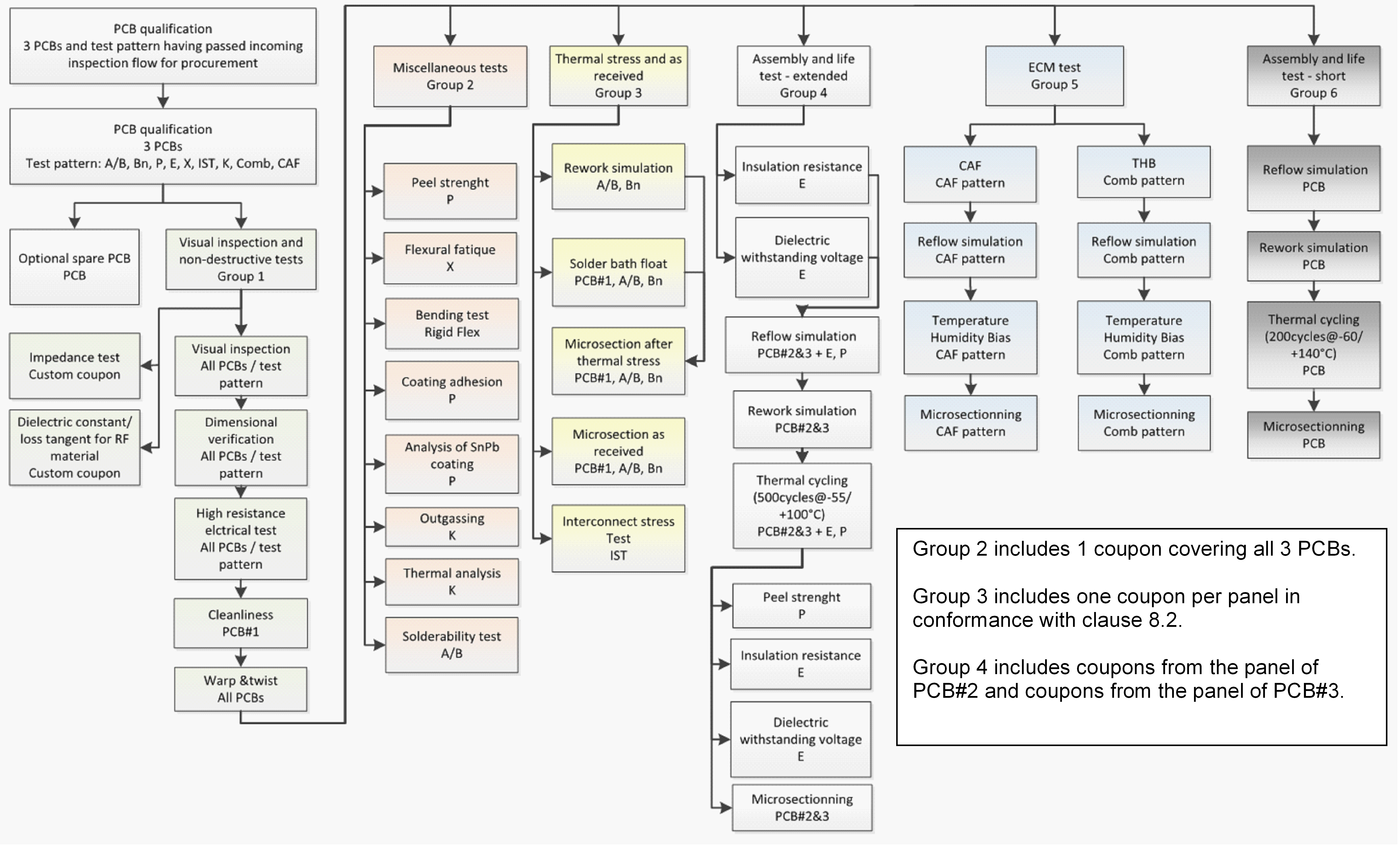 Figure 71: Test flow for qualification
Table 71: List of coupons with pattern ID, description and references to definition requirements
|
Pattern ID
|
Description
|
Requirement definition
|
|
A/B
|
combined coupon of plated-through holes (A) and through-going vias (B)
|
8.2.2c.1
|
|
Bn (=B1, B2, B3, etc.)
|
combined coupon of sequential vias (excluding through-going vias)
|
8.2.2c.2
|
|
IST
|
coupon for interconnect stress test
|
9.5.5.3
|
|
custom
|
custom coupon for impedance test
|
9.3.4
|
|
custom
|
custom coupon for dielectric constant and loss tangent
|
9.3.5
|
|
P
|
coupon for peel strength, coating adhesion and analysis of SnPb
|
9.4.2, 9.4.5, 9.4.6
|
|
X
|
coupon for flexural fatigue
|
9.4.3
|
|
rigid-flex
|
coupon or PCB for bending test
|
9.4.4
|
|
K
|
coupon for outgassing; thermal analysis, flammability, offgassing
|
9.4.7, 9.4.8, 9.4.9, 9.4.10
|
|
E
|
coupon for insulation resistance and dielectric withstanding voltage
|
9.6.3, 9.6.4
|
|
Comb
|
coupon containing comb pattern for THB test
|
9.7.2.2
|
|
CAF
|
coupon for CAF test
|
9.7.3.2
|
|
PCB#1, PCB#2, PCB#3, PCB#4
|
PCBs for visual inspection, dimensional verification, cleanliness, microsectioning as-received and after thermal stress, assembly and life testing short and extended
|
9.3.2, 9.3.3, 9.3.6, 9.5, 9.6, 9.8
|
Test selection for qualification activities
For all qualification activities, the PCBs and coupons shall be submitted to outgoing inspection and documentation in conformance with clauses 8.1, 8.2 and 8.3.
See Annex J for an overview of a qualification programme.
For initial qualification of a PCB manufacturer or a PCB technology, all tests of groups 1, 2, 3, 4, and 5 shall be performed on PCB and coupon.
For qualification renewal of a technology the following test shall be performed on PCB and coupon:
- Group 2: peel strength and solderability;
- Group 3: all. For delta qualification of a process or equipment change that affects the properties of the dielectric material, the following tests shall be performed on PCB and coupons:
- Group 1, 3, 5: all;
- Group 4 or 6: all;
- Group 2: peel strength, flexural fatigue, bending test, outgassing, thermal analysis. For delta qualification of a process or equipment change that affects the properties of the copper plating or surface finish, the following tests shall be performed on PCB and coupons:
- Group 1: visual inspection;
- Group 3: all;
- Group 4 or 6: all;
- Group 2: peel strength, solderability, analysis of SnPb coating, coating adhesion of non-fused SnPb. For delta qualification of PCB design features, the following tests shall be performed on PCB and coupons, except for track width and spacing as specified in requirement 7.2g:
- Group 1, 3: all;
- Group 4 or 6: all.
PCB design features include hole size, aspect ratio, number of layers, lamination or drilling sequences, thickness of Cu or PCB.
For delta qualification of track width and spacing, the following tests shall be performed on PCB and coupons:
- Group 1: visual inspection;
- Group 3: microsectioning as received including at least the following aspects:
- track width on foot and tolerances;
- insulation distance and tolerances;
- undercut;
- etching efficiency and absence of spurious copper;
- encapsulation of track by resin.
For qualification of HDI technology, the following tests shall be performed on PCB and coupons:
- Group 1, 3, 4, 5: all;
- Group 2: peel strength. Table 72: Test matrix for qualification and procurement
|
Scope of testing
|
Group 1
|
Group 2
|
Group 3
|
Group 4
|
Group 5
|
Group 6
|
|
Y - indicates test group to be included
| ||||||
|
Initial qualification
|
Y
|
Y
|
Y
|
Y
|
Y
|
N
|
|
Qualification renewal
|
Y
|
P
|
Y
|
N
|
N
|
N
|
|
Delta qualification
|
Y
|
P
|
Y
|
Y
|
Y
|
Y
|
|
Delta qualification
|
P
|
P
|
Y
|
N
|
N
|
Y
|
|
Delta qualification
|
Y
|
N
|
Y
|
N
|
N
|
Y
|
|
Delta qualification
|
P
|
N
|
N
|
Y
|
N
|
N
|
|
Qualification of HDI Technology
|
Y
|
P
|
Y
|
Y
|
Y
|
Y, in case of project qualification
|
|
Project qualification
|
Y
|
N
|
Y
|
N
|
N
|
Y
|
|
FAI
|
Y
|
N
|
Y
|
N
|
N
|
N
|
|
Procurement
|
Y
|
N
|
Y
|
N
|
N
|
N
|
Initial qualification of PCB manufacturer
Initial qualification of a PCB manufacturer shall be in conformance with clause 5.
The test selection for initial qualification of PCB manufacturer shall be in conformance with requirement 7.2b.
Initial qualification of PCB technology
The test selection for initial qualification of PCB technology shall be in conformance with requirement 7.2b.
The PCB manufacturer of the new technology shall already hold a qualification in conformance with clause 5.
The PCB manufacturer shall issue a new PID for the new technology to be qualified, in conformance with the requirement 5.11b.
The preparation of the microsection for the qualification of the rigid-to-flex interface shall be performed using UV fluorescent resin and vacuum potting and inspected using polarised light.
See example in Figure 85.
Qualification renewal
The test selection for qualification renewal shall be performed by the qualification authority in conformance with requirement 7.2c.
Delta qualification
The test selection for delta qualification of materials, processes, design or equipment shall be performed by the PCB manufacturer in conformance with requirements 7.2d, 7.2e, 7.2f and 7.2g.
The baseline test flow may be tailored and supplemented by additional tests to cover the delta qualification.
The delta qualification shall be in conformance with clause 5.13 and documented in the process change notice.
Upon approval of the delta qualification test report in conformance with requirements 5.10c and 5.10d, the PCB manufacturer shall document the qualified changes in the PID.
Delta qualification of track width and spacing shall include records of AOI and visual inspection on etched inner layer to check for top and bottom of track, etch definition and spurious copper in clearance.
This is performed to evaluate the efficiency of the AOI processes for its ability to detect all dimensions under delta qualification.
In case delta qualification is initiated in the context of a space project, the procurement authority shall handle it through an RFA, in conformance with clause 7.7.
Project qualification and RFA
Overview
It is preferred to use PCB technology and PCB manufacturers that are qualified in conformance with ECSS-Q-ST-70-60. Project qualification can be necessary for the use of technology that is not available from qualified sources, for instance in case innovative technology is needed. Such project qualification includes a risk to the project because the PCB technology is not widely used and because the project qualification can fail.
In case project qualification is needed, it is preferred to perform it at a PCB manufacturer that is already qualified for other technology in conformance with ECSS-Q-ST-70-60 because QA and capability has been reviewed during periodic auditing.
In case delta qualification is initiated for a space project and it is handled through an RFA, in conformance with the requirement 7.6f, it is good practice if the delta qualification for a project results in an update of the PID of the qualified PCB manufacturer. In this case, upon future procurement of the same technology, a new project qualification is not needed.
Project qualification provides approval of a PCB technology for the batch used on that project only. In case of recurrent PCB procurement, a new project qualification of the new batch is needed if the PID does not include the technology.
Project qualification typically uses a group 6 test flow which is designed to be a fast test flow on a limited number of test vehicles. This can be insufficient justification for an update of the PID depending on the technology under evaluation. Delta qualification can ensure a more thorough assignment of test flows and test vehicles with the objective to provide justification for the update of the PID.
Similarity of PCB designs covered by the project qualification can be reviewed during the DR and can result in tailoring of the project qualification test plan.
Requirements for project qualification and RFA
PCB technology that is not qualified in conformance with requirement 5.1a shall be subject to project qualification for each batch using an RFA in conformance with clause 5.4.2 from ECSS-Q-ST-70.
Project qualification shall provide approval of a PCB technology for the batch used on that project only.
In case of recurrent PCB procurement, a new project qualification of the new batch shall be performed if the technology is not included in the PID in conformance with ECSS-Q-ST-70-60.
* It is, therefore, good practice to perform delta qualification of a qualified PCB manufacturer and update its PID, in conformance with requirement 7.7.2o.
Before the PCB procurement, the procurement authority shall submit to its customers for approval the RFA part 1 including the following:
- PCB approval sheet in conformance with Annex G;
- Compliance matrix to ECSS-Q-ST-70-60 for PCB qualification and description of the non-qualified aspects;
- Compliance matrix to ECSS-Q-ST-70-12 for PCB design;
- Compliance matrix to the PID from the PCB manufacturer;
- Compliance to inspection on PCB and coupon for procurement in conformance with clause 8.
- Description of the thermal, electrical and mechanical environment of the application;
- Project qualification test plan;
- Technical justification in case a single PCB design is intended to cover several PCBs to be used for the project;
- Verification and inspection to be performed in case several batches are manufactured to cover for the qualification vehicle and the FMs.
- 1 See Annex J for an overview of a qualification programme.
- 2 The verification for batch-to-batch reproducibility from 7.7.2d.9 can include a project audit, dedicated evaluation on coupons or group 6 on spare PCBs. This is important for PCB manufacturers that are not qualified in conformance with ECSS-Q-ST-70-60 as described in the note of requirement 7.7.2e.
The group 6 from the qualification test plan should be performed on one spare PCB from the FM batch.
The advantage of testing the FM batch is to ensure representativity. This is important when using non-qualified PCB manufacturers for whom batch-to-batch QA has not been verified by an audit in conformance with ECSS-Q-ST-70-60. The disadvantage of testing the FM batch is that any nonconformances are discovered at a late stage of the procurement.
Non-qualified PCB technology should be procured from a PCB manufacturer that is qualified in conformance with ECSS-Q-ST-70-60 for other technology.
In this case only a delta qualification can be performed for the specific technology feature that is not qualified. This reduces the risk, since other technologies are already qualified and periodic auditing has been performed.
The project qualification test plan shall include tests and inspections to evaluate all PCB technology features under qualification.
The project qualification test plan shall include group 6 in conformance with clause 9.8 and be tailored for the following:
- qualification status of the PCB manufacturer in conformance with ECSS-Q-ST-70-60;
- specific project requirements;
- PCB technology features under qualification.
The test selection specified in clause 7.2 can be used as a guideline for the project qualification test plan.
The project qualification test plan may include specific evaluations on coupons and non-destructive inspection on PCBs.
The project qualification test plan shall include IST testing in conformance with clause 9.5.5 in case the PCB technology is within the technology perimeter of IST.
DR shall be performed in conformance with 6.2.5a with support of the PCB manufacturer to review the manufacturability and reliability of the design and to review previous heritage and test campaigns performed.
The DR should be performed together with the final customer.
In case risk factors are identified during DR, specific tests and inspections shall be specified in the project qualification test plan to mitigate the risk.
After PCB procurement, the procurement authority shall submit to its customers for approval the RFA part 2 including the following:
- project qualification test report;
- test report for specific evaluation on coupons and PCBs in conformance with 7.7.2i and 7.7.2j;
- outgoing inspection on PCB and coupons in conformance with 8.1 and 8.2;
- CoC and its lab reports in conformance with 8.3a;
- incoming inspection in conformance with 8.4.
In case delta qualification is initiated for a space project under RFA in conformance with the requirement 7.6f, the project qualification should result in an update of the PID of the qualified PCB manufacturer.
In case suppliers use IPC standards as PCB procurement specification, all the following conditions shall be met: - The project qualification is performed using group 6 in conformance with clause 7.7.2.
- The PCB design is in conformance with chapter 6.3 from IPC-2221B for electrical clearance.
- IPC-6012D and IPC-6012DS for space applications are used for rigid PCBs.
- IPC-6018C and IPC-6018CS for space applications are used for RF PCBs.
- IPC-6013D is used for flexible and rigid-flex PCB.
- PCB manufacturers are on the IPC QML or have passed a specific audit from the procurement authority to assess compliance to the IPC standards from conditions 3, 4 and 5.
- Coupons and PCBs of all panels are evaluated in conformance with clause 8.
- Coupon inspection is performed by a third-party lab for evaluation in conformance with IPC-A-600 and the applicable IPC standards from conditions 3, 4 and 5.
- 1 For requirement 7.7.2p.1 during the project qualification, any HDI technology or embedded film components are evaluated.
- 2 Requirement 7.7.2p.1 is in conformance with IPC-6011 clause 3.6 which specifies that the qualification assessment is as agreed between user and supplier (AABUS).
- 3 Requirement 7.7.2p.2 is particularly important in case double insulation is applicable. However, IPC-2221B is not necessarily meeting the requirements from ECSS-Q-ST-70-12 for double insulation. It is good practice to implement the additional risk mitigations for double insulation in conformance with the present standard and ECSS-Q-ST-70-12. In case the PCB design is not performed as per ECSS-Q-ST-70-12 as described in requirement 7.7.2p.2, it is good practice to provide a compliance matrix to insulation distance for double insulation from clause 13.9 of ECSS-Q-ST-70-12 and requirements 6.5c and 8.5c of ECSS-Q-ST-70-60.
- 4 For requirement 7.7.2p.3 it is not good practice to use only IPC-6012D class 3, which represents a lower quality class.
- 5 For requirement 7.7.2p.5 it is good practice to use IPC-6013DS for space applications when this is issued.
- 6 The evaluation from requirement 7.7.2p.7 includes the following:
- coupon evaluation includes IST testing in conformance with clause 9.5.5 when this is applicable to the technology,
- coupon evaluation includes three times solder bath float test and rework simulation, among others,
- PCB visual inspection is performed using 10-40x magnification,
- PCB evaluation includes high resistance electrical test with 1 GΩ insulation resistance threshold.
Test and inspection for procurement
Outgoing inspection on PCB
The PCB manufacturer shall submit PCBs to outgoing inspection as follows:
- visual inspection in conformance with clause 9.3.2;
- dimensional verification in conformance with clause 9.3.3.1;
- warp and twist in conformance with clauses 9.3.3.2 and 9.3.3.3;
- high resistance electrical test and continuity test in conformance with clauses 9.3.7 and 9.3.8. The sample plan for the outgoing inspection from requirement 8.1a shall be in conformance with Table 81.
Table 81 specifies sampling on external layers of PCBs during outgoing visual inspection. Internal layers are inspected during microsectioning for outgoing inspection as specified in clause 8.2. In addition some in-process inspections are specified in clause 6.3.
The PCB manufacturer and procurement authority may specify a more frequent sampling plan or additional measurement locations in the PCB definition dossier.
This can be the case if a review item has been identified during MRR, for instance for the compliance of dimensional aspects. This can be the case for small connectors using small diameter PTH that can be blocked with SnPb. This can also be the case when board geometry is critical for placement in an electronic box. Some designs can specify the thickness over metallisation. Some designs can have complex geometry due to rigid-flex or cut-outs.
The PCB manufacturer shall perform referee testing on a spare PCB in case this is specified in Table 1026 and 10.6.3c.
Referee testing is specified in Ref. b and c from Table 1026.
The presence of coupons, the evaluation of coupons, the delivery of coupons to the customer and the delivery of microsection to the customer shall be in conformance with Table 82.
Table 81: Sampling plan for outgoing visual inspection on PCB
|
Test method and inspected feature
|
Sampling
|
|
Visual inspection
|
all PCBs and coupons
|
|
Dimensional verification:
|
1 PCB per panel
|
|
Dimensional verification:
|
1 PCB from the batch
|
|
Dimensional verification:
|
1 PCB from the batch
|
|
Dimensional verification:
|
1 PCB from the batch
|
|
Dimensional verification:
|
1 PCB from the batch that is worst-case
|
|
High resistance electrical test and continuity test
|
all PCBs and coupons
|
Outgoing inspection on coupons
Overview
This clause describes the test flow, coupon configuration and inspection methods on coupons and PCBs for procurement. Table 82 and Figure 81 shows a non-exhaustive overview of coupons and tests specified in this clause. This table shows when evaluations are performed.
Table 82: Overview of coupons
|
Set ID
|
Location
|
Feature and name of coupon as per IPC-2221B
|
Test
|
Condition for presence of coupon
|
Condition for evaluation of coupon
|
Coupon delivered to customer
|
Microsection delivered to customer
|
|
set 1
|
one corner
|
PTH and via on A/B
|
AR + RW
|
yes
|
yes
|
no
|
yes
|
|
sequential via on Bn
|
AR
|
yes
|
yes
|
no
|
yes
| ||
|
PTH and via on A/B
|
customer coupon
|
yes
|
yes
|
yes
|
no
| ||
|
sequential via on Bn
|
customer coupon
|
yes
|
yes
|
yes
|
no
| ||
|
tracks on A/B
|
min track width and spacing
|
yes
|
optional
|
yes
|
optional
| ||
|
set 2
|
opposite corner
|
PTH and via on A/B
|
SB
|
yes
|
yes
|
no
|
yes
|
|
sequential via on Bn
|
SB
|
yes
|
yes
|
no
|
yes
| ||
|
PTH and via on A/B
|
customer coupon
|
yes
|
yes
|
yes
|
no
| ||
|
sequential via on Bn
|
customer coupon
|
yes
|
yes
|
yes
|
no
| ||
|
tracks on A/B
|
min track width and spacing
|
yes
|
optional
|
yes
|
optional
| ||
|
set 3
|
anywhere
|
PTH on A/B
|
solderability
|
yes
|
yes for SnPb < 1 µm
|
yes
|
n.a.
|
|
set 4
|
4 corners
|
electrical registration on R
|
electrical registration
|
yes for annular ring < 50 µm
|
yes
|
yes
|
n.a.
|
|
set 5
|
as per 9.5.5.3d, e and f
|
IST coupon
|
IST test
|
yes for applicable technology
|
yes
|
yes
|
optional
|
|
set 6
|
anywhere
|
peel strength on P
|
peel strength
|
yes
|
optional
|
yes
|
n.a.
|
|
coating adhesion on P
|
tape test
|
yes
|
optional
|
yes
|
n.a.
| ||
|
flex bend cycles on X
|
bend test
|
yes for applicable technology
|
yes
|
optional
|
optional
| ||
|
rigid-flex interface on X
|
SB
|
yes for applicable technology
|
yes
|
no
|
yes
| ||
|
set 7
|
anywhere
|
insulation resistance on E
|
insulation resistance
|
yes
|
optional
|
yes
|
n.a.
|
|
DWV on E
|
DWV
|
yes
|
optional
|
yes
|
n.a.
| ||
|
controlled impedance on Z
|
controlled impedance
|
yes for applicable technology
|
optional
|
optional
|
n.a.
| ||
|
embedded film resistance
|
resistance
|
yes for applicable technology
|
optional
|
optional
|
optional
| ||
|
set 8
|
anywhere
|
pure laminate
|
thermal analysis
|
yes
|
optional
|
yes
|
n.a.
|
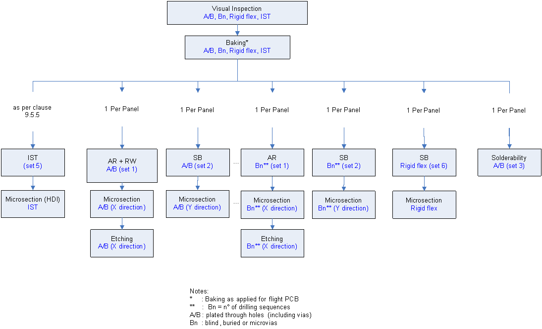 Figure 81: Flow for preparation, test and inspection of procurement coupons
Configuration of coupons for plated holes
The preparation, test and inspection of procurement coupons shall be in conformance with Figure 81.
Coupons shall be designed in conformance with clause 15 of ECSS-Q-ST-70-12.
Each panel shall include the following coupons for plated holes:
- Coupon A/B;
- Coupon B1, B2… Bn.
These coupons can be designed in accordance with IPC-2221B. However, other custom designs are used that cover the same features.
Coupon A/B shall include the following features:
- PTH with maximum or most frequently used diameter;
- through-going via with minimum diameter.
- 1 For 8.2.2d.1 coupon A of IPC-2221B can be used, and for 8.2.2d.2 coupon B of IPC-2221B.
- 2 Plated holes for mechanical purpose are not represented in coupons. Risks associated with mechanical drilling are mitigated by visual inspection, high resistance electrical testing and process audit. In case of specific criticality of mechanical holes, the PCB procurement authority can add a coupon for it in the PCB definition dossier.
Coupon A/B shall include at least 4 holes per drilling sequence.
Coupon Bn shall include at least 3 holes per drilling sequence.
See an example of 3 holes per drilling sequence for coupon Bn in Figure 82. The top layer is a different drill sequence than the bottom layer and therefore 3 holes are present in the coupon for both layers.
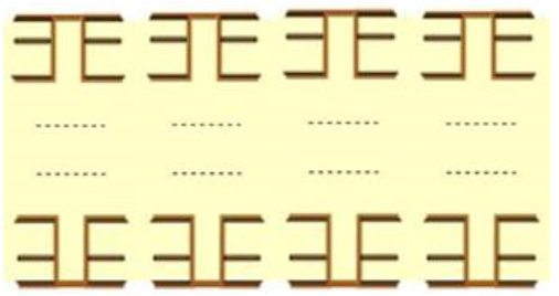 Figure 82: Example of Bn coupon with 3 holes per drilling sequence
Coupon Bn shall include the following features:
- blind via for each plating sequence with minimum diameter;
- buried via for each plating sequence with minimum diameter;
- microvia for each plating sequence with minimum diameter.
This is coupon B1, B2, etc. of IPC-2221B.
The suffix of coupon B1, B2… Bn shall indicate the plating sequence of the vias that are included.
An example of vias manufactured at different plating sequences is shown in Figure 84.
The term “coupon Bn” shall indicate all coupons B1, B2 … Bn for all plating sequences.
Coupons for plated holes shall include rows and columns of holes to enable microsectioning of a coupon in both X-direction and Y-direction.
The IPC coupons are designed in a square.
In case superpositioned blind vias are present in the PCB it shall be included in the design of the coupon Bn.
At least two coupons for plated holes shall be placed on opposite corners of the panel to enable assessment of annular ring in both corners.
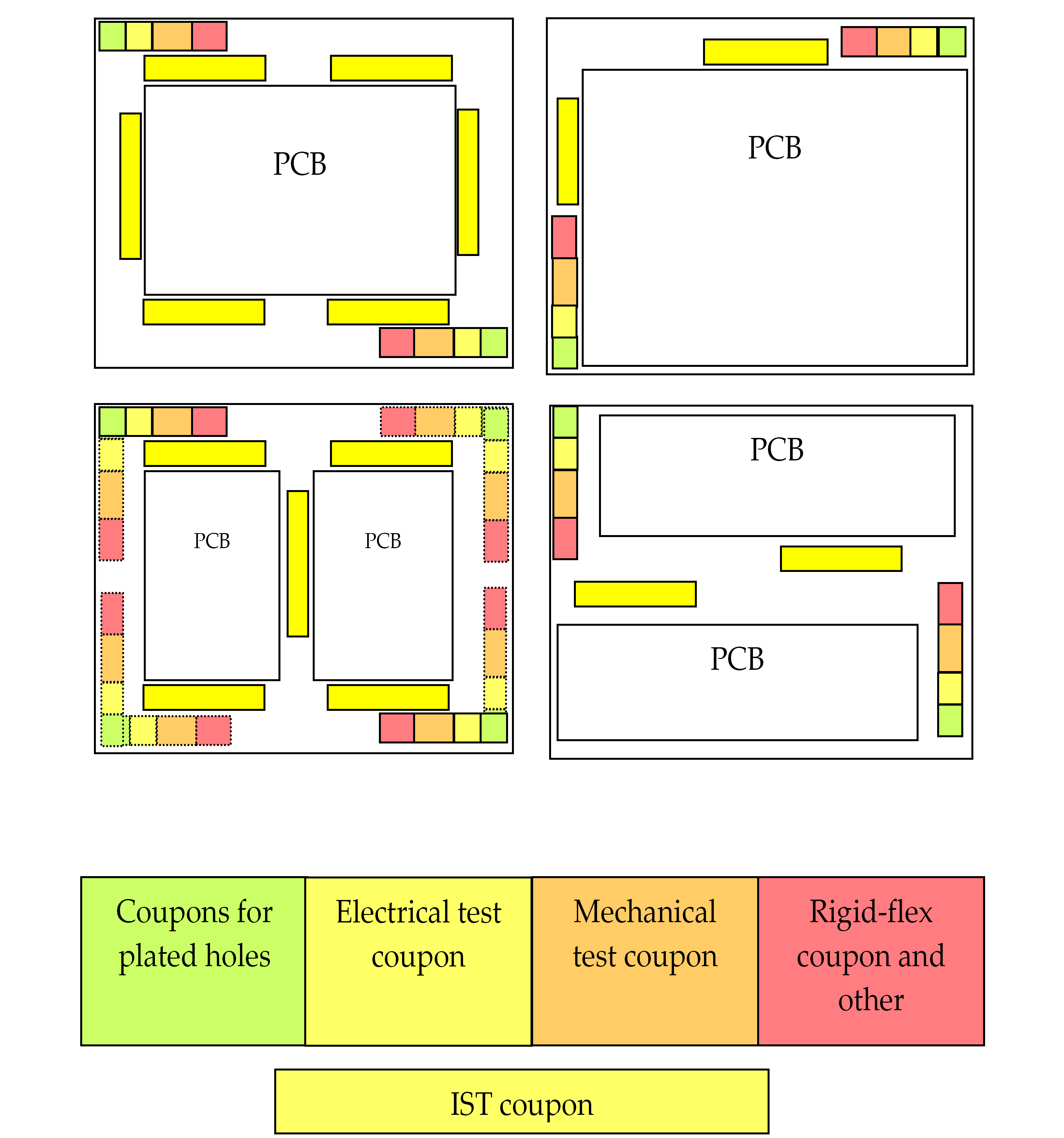 Figure 83: Example of placement of coupons and PCB in usable area of manufacturing panel
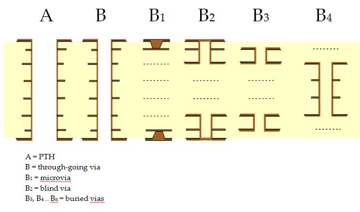 Figure 84: Example of vias manufactured at different plating and drilling sequences
Configuration of dedicated coupons
In case the technology is within the technology perimeter for IST as specified in the clause 9.5.5.2, the IST coupon shall be designed and tested in accordance with clause 9.5.5.
In case of a rigid-flex PCB, a coupon with rigid-to-flex interface shall be included on each panel.
It is good practice to include in this coupon the via nearest to the rigid-to-flex interface.
For designs with reduced annular ring of 25 µm in conformance with requirement 11.5.2a of ECSS-Q-ST-70-12, electrical registration coupons shall be included on all four corners to verify the annular ring.
This is coupon R of IPC-2221B. Alternatively, a dedicated pattern can be available on IST coupons.
A coupon shall be present for solderability testing.
- 1 This can be achieved by repeating the A/B coupon of IPC-2221B.
- 2 Performing solderability testing is specified in case SnPb < 1 µm in conformance with Table 1012.
In case more than one PCB is placed in the panel, a coupon for evaluation of plating should be placed in the middle of the panel.
A coupon for plating can be an IST coupon, A/B coupon or a spare PCB. An example of coupon placement in the centre of the panel is shown in Figure 83.
If embedded film resistors are used, they shall be included in the coupons, in conformance with requirement 15.2d.13 of ECSS-Q-ST-70-12.
If controlled impedance is used, it shall be included in the coupons, in conformance with requirement 15.2g of ECSS-Q-ST-70-12.
Commonly used test probes need a coupon to verify controlled impedance. Some advanced test probes are available, however, that allow testing on the PCB.
A coupon shall be present that include minimum track width and spacing on each layer, in conformance with requirement 15.2d.9 of ECSS-Q-ST-70-12.
It is good practice to include minimum track width and spacing in the A/B coupon for plated holes.
A coupon shall be present that include patterns for mechanical tests in conformance with requirement 15.2f.2 of ECSS-Q-ST-70-12.
Mechanical tests include peel strength and coating adhesion. Flex bend cycles can be performed on the coupon with rigid-to-flex interface of requirement 8.2.3b.
A coupon shall be present that includes patterns for electrical tests in conformance with requirement 15.2f.3 of ECSS-Q-ST-70-12.
Electrical tests include insulation resistance, dielectric withstanding voltage. Specific electrical test conditions can be specified by the procurement authority in conformance with requirement 9.6.3d.
A coupon shall be present to perform thermal analysis.
- 1 The coupon can be an area of approximately 1x1 cm without copper and without vias.
- 2 Thermal analyses are used to investigate stability of materials, processes and design. Strict acceptance criteria can be unavailable in which case the test is evaluated against the heritage and datasheets or used for failure investigation.
Evaluation of coupons
All coupons shall be evaluated by visual inspection, in accordance with requirements from clause 9.3.1 and 9.3.2.
Evaluation of acceptance criteria for visual inspection and microsectioning shall be performed in accordance with requirements from clause 10.
The coupons specified in requirements 8.2.3d, 8.2.3h, 8.2.3i, 8.2.3j and 8.2.3k may remain untested for procurement.
Coupons for plated holes shall be submitted to microscopic inspection in the following conditions:
- each hole type: as received;
- each hole type: solder bath float in accordance with clause 9.5.2;
- at least one PTH: rework simulation in accordance with clause 9.5.4.
The holes adjacent to the one submitted to RW are considered to be in as-received condition. This allows assessment of both conditions in a single microsection.
Microsectioning on coupon A/B shall be performed on at least 4 holes per drilling sequence and on coupon Bn on at least 3 holes per drilling sequence.
See Figure 82 for an example of drilling sequence of holes.
The microsectioning of coupons for plated holes of each hole type shall be performed in both X-direction and Y-direction for assessment of annular ring in both directions.
To reduce the number of coupons and microsections, it is common practice to microsection the thermally stressed coupon in perpendicular direction to the as received coupon.
The microsections of the as-received coupons for plated holes shall be submitted to microscopic inspection in as-polished and micro-etched conditions.
The microsection of the thermally stressed coupons for plated holes shall be submitted to microscopic inspection in as-polished condition.
This is specified because micro-etch reveals the interface between plated copper layers. Therefore this is less efficient to evaluate any plating separation.
Solderability test shall be performed for procurement, except in case of requirement 8.2.4j.
Solderability test need not to be performed for procurement in case all the following conditions are met:
- The surface finish is hot oil reflowed SnPb;
- The thickness of the SnPb as specified on the CoC of the panel is in conformance with the requirements of Table 1012;
- The PID does not specify that solderability testing is mandatory for procurement.
In case the thickness of SnPb is not in conformance with the requirements of Table 1012 as determined during qualification (renewal), the PID can specify that solderability test is performed for all procurement. This is usually the case upon request by the qualification authority.
The microsection of the coupon with the rigid-to-flex interface shall be submitted to microscopic inspection after solder bath float, in as-polished condition.
The preparation of the microsection of the coupon with the rigid-to-flex interface should be done using UV-fluorescent resin and vacuum potting and inspected using polarised light.
This is mandatory for qualification as specified in requirement 7.4d.
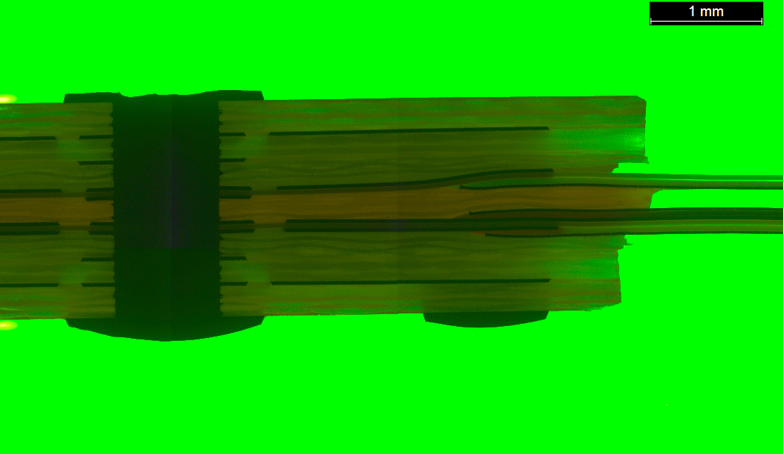 Figure 85: Example of target quality of microsection of rigid-flex interface with UV fluorescent resin and polarised light
Delivery of coupons, microsections and spare coupons
Coupons shall be delivered to the procurement authority in conformance with the Table 82.
The IST coupon may be send later than the other coupons, due to its logistics of test and shipment.
The following microsections shall be delivered to the procurement authority:
- Microsections of coupons for plated holes;
- Microsections of coupon for rigid-to-flex interface.
This is summarised in Table 82.
Reporting of outgoing inspection and delivery
The PCB manufacturer shall report the results of the outgoing inspection on PCB and coupons in the lab reports of the CoC, in conformance with the DRD of Annex B.
100 % visual inspection of PCBs is specified in requirement 8.1a.1, whereas the lab report specifies the requirements for the documentation of the visual inspection.
The CoC and its lab reports shall be delivered to the procurement authority.
The PCB manufacturer shall not deliver a PCB with nonconformances to ECSS-Q-ST-70-60.
The PCB manufacturer shall not deliver without approval from the procurement authority a PCB with nonconformances to the PCB definition dossier.
This includes definition of holes, milling, non-plated holes, dimensional and mechanical requirements, among other things as described in the DRD of Annex A of ECSS-Q-ST-70-12.
Incoming inspection by procurement authority
The procurement authority shall perform incoming inspection as follows:
- Visual inspection on all PCBs, in conformance with the clause 9.3,
- Microscopic inspection on microsections, in conformance with the clause 10, by one of the following institutes:
- procurement authority;
- external third-party lab;
- assembly house;
- PCB manufacturer using another inspector than the one for outgoing inspection.
- Verification of the CoC and its lab reports, in conformance with the Annex B,
- Verification of quantity,
- Verification of integrity of packaging.
- 1 The PCB manufacturer provides microsections used for the CoC and customer coupons. Both can be used for the incoming inspection. To avoid deterioration of the surface quality of microsections, it is preferred to perform incoming inspection as soon as possible after delivery.
- 2 Microsection inspection for qualitative aspects is important and detection can be operator dependent. Therefore this requirement specifies to perform an additional verification.
The procurement authority need not to perform microscopic inspection of the microsection of the reworked hole in as-polished condition.
This is specified because the microsection with the reworked hole includes other holes as-received. These as-received holes are inspected as-polished and after micro-etching. The procurement authority can only inspect in as-polished condition by repolishing the etched section.
The procurement authority shall maintain records of the accepted incoming inspection.
Records of incoming inspection are made available during equipment MRR as specified in 6.14t.
In case of nonconformances during incoming inspection an NCR shall be issued by the procurement authority to the PCB manufacturer.
The procurement authority may perform incoming inspection at their own premises or at the premises of the PCB manufacturer.
If performed at the premises of the PCB manufacturer, the inspection is typically named: FCSI or MIP or DRB or buy-off.
The procurement authority shall complete the incoming inspection within 3 months after availability of the PCBs.
FAI on PCB by microsectioning
When specified, FAI on PCB shall include the microsectioning of a representative PCB from the batch for the first procurement.
FAI is performed in supplement of the standard outgoing and incoming inspection on PCBs and coupons.
FAI on PCB shall be performed in case this is specified by the procurement authority.
FAI on PCB shall be performed in case double insulation applies, in conformance with the requirement 13.9.2d of ECSS-Q-ST-70-12.
FAI on PCB should be performed in case the PCB design is complex and the coupon cannot be designed with full representativity, in conformance with the requirement 15.2b of ECSS-Q-ST-70-12.
FAI on PCB should be performed on a representative PCB from the batch for the first procurement, if a technology is procured from a PCB manufacturer for the first time.
During FAI on PCB, the microsectioning shall verify the technology features that are procured for the first time.
In case of FAI on PCB, it shall be performed and documented by the procurement authority within 4 months after availability of the PCBs, by using one of the institutes specified in requirement 8.4a.2.
The documentation of FAI on PCB shall be provided by the procurement authority to the PCB manufacturer.
- 1 It is important for the PCB manufacturer to have the feedback from the FAI.
- 2 FAI is reviewed during MPCB as specified in requirement 6.14r.
Test descriptions
Overview
This clause describes the test methods for the groups 1 to 6. An overview of this is shown in Figure 71.
Some test methods can include acceptance criteria. Test methods that include visual inspection of PCBs and coupons, and microscopic inspection of microsections have acceptance criteria specified in clause 10.
Examples of test patterns and coupons are included in each test method. Reference is made to test patterns from IPC-2221B. In future it is expected that other IPC standards also include test patterns.
Additional tests
Cleanliness
The cleanliness of the samples prior to test and inspection shall be in conformance with 6.11a.
In case samples need to be cleaned, a cleaning method is specified in clause 11.1 of ECSS-Q-ST-70-08.
Bake-out
Standard bake-out shall be minimum 8 hours at 120 ˚C in ambient pressure.
- 1 Baking is performed to remove humidity from the dielectric materials prior to thermal excursions. PCB laminates are known to be hygroscopic.
- 2 For sensitive PCB technology such as rigid-flex, this bake-out can cause damage when the heating rate is high. In this case a tailoring of the bake-out profile is good practice as per requirement 9.2.2b.
- 3 This bake-out is in conformance with clause 8.5d of ECSS-Q-ST-70-38.
In case the PCB technology or the test criteria are affected by humidity, the bake-out may be tailored to improve its efficiency.
Improving efficiency of the bake-out can be established by a longer duration, vacuum or dry environment or a stepped baking profile. This can be necessary for thick PCBs, a high number of copper plane layers, flex laminate layers or samples stored in non-controlled environment. Tests that can be significantly affected by humidity include thermal excursions and high resistance electrical test.
The PCB manufacturer may tailor the bake-out in case samples are processed immediately after reflow as a final process step.
After bake-out, re-absorption of humidity shall be prevented until thermal stress testing.
Precautions can include short duration (for example less than 8 hours) of storage between bake-out and thermal stress test or storage in dry conditions.
Plated copper tensile strength and elongation
Plated copper tensile strength and elongation shall be performed in conformance with test method 2.4.18.1a from IPC-TM-650 or an equivalent test method.
Plated copper tensile strength shall be ≥ 276 MPa.
Plated copper elongation shall be ≥ 18 %.
Steam ageing
When performed, the steam aeging test shall be carried out in conformance with test 20a of IEC 60326-2-am 1 (1992-06).
This test method was specified in ECSS-Q-ST-70-10 and is included here for completeness. However, it is not included in any of the test groups. The test is intended to give an indication of the effects of storage on the solderability of the PCBs. Steam ageing is also described in paragraphs 3.4.3 and 3.4.4. of IPC-J-STD-003C.
The specimen shall be exposed in the steam generator machine for approximately 80 minutes.
After closing the generator, it shall be purged with nitrogen at a flow rate between 250 ml/minute and 750 ml/minute.
The temperature inside machine shall be (100 2) C and stabilized for (5 1) minutes.
The nitrogen flow shall be switched off.
The 90 C condensed steam rate in the chamber shall be controlled to (5 0,5) l/minute.
A mixture of pure oxygen 20 % and nitrogen 80 % with a flow rate of (100 10) ml/minute shall be switched on for (60 5) minutes.
After removing the specimens from the steam generator machine, they shall be dried.
Group 1 – Visual inspection and non-destructive tests
Visual inspection - general
Visual inspection shall be performed using 10x to 40x magnification.
Examples of equipment used for visual inspection are: binoculars, loups, single scope.
Visual inspection shall cover the entire surface of both sides of the sample.
Visual inspection shall be performed using high illuminating light sources.
ECSS-Q-ST-70-08 clause 5.4.a requires 1080 lux. However, higher intensities are typically used for bare board inspection.
In case of any suspected nonconformance, the area shall be re-examined at higher magnification of 20x to 40x.
Visual inspection for qualitative aspects
Visual inspection for qualitative aspects shall be performed on PCB and coupons for conformance with acceptance criteria from clauses 10.4 and 10.5.
Visual inspection for dimensional verification
General
Physical dimensions shall be measured for verification of the PCB definition dossier.
- 1 In addition to the specified measurement, the physical dimensions are also submitted to visual inspection in conformance with clause 9.3.2.
- 2 The mechanical drawing is typically used to specify physical dimensions and tolerances of the PCB.
PCB thickness shall be measured over base laminate on corners and on the middle of the PCB, unless another methodology is specified in the PCB definition dossier.
Length and width of the PCB shall be measured over all edges of the inspected PCB.
The diameter of plated and non-plated holes shall be verified for all hole diameters.
The number of hole diameters for verification on the inspected PCB shall be specified by the PCB manufacturer.
Hole diameters can be measured with measuring gauges, a measuring microscope or dedicated automatic systems.
Vias of < 0,6 mm may be omitted during dimensional verification of its diameter, unless dimensional verification of these holes is specified in the PCB definition dossier.
This is because these holes can be blocked with SnPb in conformance with requirement 10.6.3g.
Minimum conductor width and spacing shall be measured on external layers.
- 1 Conductors include tracks and SMD pads.
- 2 Conductor width and spacing on internal layers are present on the coupon in conformance with 8.2.3h for optional evaluation by microsectioning. Minimum track width and spacing on internal layers are evaluated by in-process inspection in conformance with 6.3f.3.
Minimum conductor width and spacing shall be measured at the foot of the conductor, except for the case specified in requirements 9.3.3.1i and 9.3.3.1j.
An example of conductor width measured at the foot is shows as seen in a cross-section in Figure 91.
In case overhang or undercut causes the top of the conductor to protrude from the foot, conductor width and spacing shall be measured at the widest point of the conductor.
In case of RF PCBs the conductor width may be measured in conformance with the PCB definition dossier.
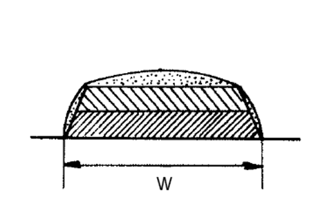 Figure 91: Conductor width (w) measured at the foot as seen in a cross-section.
Warp
Warp shall be measured in conformance with the test method 2.4.22c from IPC-TM-650.
“Bow” is a term that is synonymous to “warp”.
The PCBs shall be placed unrestrained on a horizontal surface with the convex side upward.
The two corners of the measured edge shall be in contact with the horizontal surface.
The maximum distance between the horizontal surface and the PCB shall be measured as specified in Figure 92.
The length of the PCB shall be measured.
The warp shall be expressed in percentage terms.
Warp shall be calculated as follows:
- Warp [%] = max distance [mm] / length of PCB [mm] x 100
The maximum warp shall be 1,5 %.
The procurement authority may specify a more stringent requirement for warp in the PCB definition dossier. - 1 A typical stringent warp and twist requirement is 0,75 %, which is in conformance with IPC-6012DS reference 3.4.3.
- 2 This can be done for complex assembly, such as large components without stress relief, where less warp and twist can avoid stress on component assembly.
- 3 Warp and twist are strongly affected by the symmetry of the build-up. In case the PCB is designed with asymmetric build-up in conformance with requirements 7.1.1a, 7.1.1b, 7.1.2a and 7.1.2d from ECSS-Q-ST-70-12, the procurement authority and PCB manufacturer mutually define the value of max warp in the MRR and in the PCB definition dossier. This agreed value cannot exceed 1,5 % in conformance with requirement 9.3.3.2h.
- 4 On PTFE-based laminates it is not applicable to measure warp and twist because of the material softness.
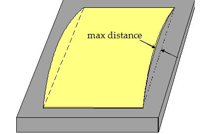 Figure 92: Warp
Twist
Twist shall be measured in conformance with the test method 2.4.22c from IPC-TM-650.
The PCB shall be placed on a horizontal surface so that it rests on three corners.
In case three corners cannot rest on the horizontal surface by restraining only one corner, the referee test shall be performed in conformance with chapter 5.3 of the test method 2.4.22c from IPC-TM-650.
The distance between the horizontal surface and the fourth corner of the PCB shall be measured as specified in Figure 93.
The length of the diagonal of the PCB shall be measured.
The twist shall be expressed in percentage terms.
Twist shall be calculated as follows:
- Twist [%] = max distance [mm] / (2 x length of PCB diagonal [mm]) x 100
The maximum twist shall be 1,5 %.
The procurement authority may specify a more stringent requirement for twist in the PCB definition dossier. - See the notes 1, 2, 3 and 4 from clause 9.3.3.2.
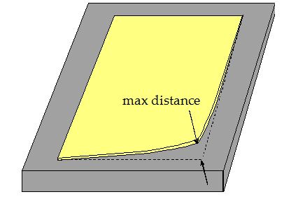 Figure 93: Twist
Impedance test
Impedance test for controlled impedance lines shall be performed using TDR in conformance with test method 2.5.5.7a of IPC-TM-650.
The measurement method for impedance test shall be specified by the procurement authority in the PCB definition dossier.
This includes nominal impedance and tolerances, transmission line types and reporting. Typical acceptable tolerance can be 10%. DC resistance compensation can be used.
Impedance test may be performed on specific coupons or on PCB.
Specific equipment and training is needed for impedance testing on PCB. It can be difficult to design an impedance coupon that is representative of the PCB. Therefore, this measurement is typically performed on the PCB.
Dielectric constant and loss tangent
Dielectric constant and loss tangent of RF materials shall be measured on specific coupons in conformance with test method 2.5.5.2a of IPC-TM-650.
The measurement method for dielectric constant and loss tangent shall be specified by the procurement authority in the PCB definition dossier.
This includes tolerances and reporting.
Cleanliness
Cleanliness testing of PCB shall be performed in conformance with clause 11.3 of ECSS-Q-ST-70-08 and test method 2.3.25.1 from IPC-TM-650.
The cleanliness value shall be ≤ 1,56 µg NaCl eq /cm2.
- 1 This value is historically driven by the limit for an assembled PCB. However, the cleanliness of a bare PCB is typically orders of magnitude better. Nevertheless, a more stringent value is not specified. It is good practice to have a cleanliness value of ≤ 0,1 µg NaCl eq /cm2.
- 2 Guidelines for cleanliness of bare PCB and assembled PCB are given in IPC-5703 and IPC-5704.
High resistance electrical test
Overview
PCBs can fail due to latent short circuits. It is acknowledged that random contamination inside the dielectric PCB material is of concern, as discussed in clause 6.7. Contamination can comprise of fibres in laminate or on prepreg layers and can originate from the PCB manufacturing processes or from the base material supply chain. The presence of contamination can provide a pathway for leakage current and possible ECM.
Typical electrical testing applied on PCBs by a flying probe equipment, is specified in IPC-9252B and is based on an insulation threshold of 10 MΩ, corresponding to level C for IPC-6012D class 3. The objective of this test method is to verify electrical design, i.e. the absence of unintended connections in the circuit. For IPC-6012DS this test method is amended to 100 MΩ under 250 V bias.
The purpose of the high resistance electrical test method is to determine the quality of the insulation and possible imperfections in the dielectric material. The rationale is that contamination between nets can provide a high-Ohmic path that can be detected under high voltage bias and therefore fails this test. On PCBs that fail the high insulation requirement, it has been demonstrated by DPA that the high-Ohmic path was caused by contamination in the dielectric material.
Clause 9.6.3 requires insulation resistance of ≥1 GΩ (and orders of magnitude higher) for interlayer and intralayer on dedicated test patterns. The requirement for high insulation is further substantiated by the typical volume resistivity of dielectric materials in the order of 108 MΩ-cm, determined at humid conditions of 90% RH in accordance with test method 2.5.17.1 of IPC-TM-650.
It is not the purpose of the high resistance test method to stress the dielectric material by screening for the operational voltage with a specified margin. For operational voltages higher than the test voltage (of 250V), a specific test can be specified by the procurement authority in the PCB definition dossier, such as a dielectric withstanding voltage test. The high test voltage of 250 V is applied because it is necessary to generate a leakage current that can be detected by the test equipment and that corresponds to a high insulation threshold of 1 GΩ.
Application of the test voltage of 250V on the smallest insulation distance for standard as well as HDI technology results in a worst-case electrical field of approximately 3 kV/mm. This is acceptable for the purpose of this high resistance test, because of the heritage with this test voltage on PCBs, the electrical strength specified in datasheets in the order of ≥30 kV/mm and the short duration of the sustain time.
Precautions, such as dehumidification of air, are needed to prevent discharge due to ionisation of air, which has a breakdown strength of 1.5-3.0 kV/mm depending on humidity. This is important for surface conductors spaced approximately 170 µm or closer.
High resistance electrical test method
High resistance electrical test shall be performed on final PCBs using flying probe equipment.
The test voltage shall be ≥ 250 V.
The insulation threshold shall be ≥ 1 GΩ.
The sustain time shall be ≥ 5 ms.
It is common that the sustain time is more than 5 ms to allow the voltage ramp up, especially in case large ground layers are present.
During the ramp-up from 0 V to 250 V, the test voltage shall be monitored.
Lack of voltage stability during the sustain time and during the ramp-up shall be recorded as test failure.
The horizontal adjacency distance shall be ≥ 1,27 mm in-plane.
The vertical adjacency distance shall be ≥ 1,27 mm in-plane on the layers above and below the specified net.
Horizontal and vertical adjacency is specified as a distance in-plane of the PCB to the tested net. This is illustrated in Figure 94.
Direct resistive isolation testing shall be performed.
Indirect isolation testing by signature comparison shall not be performed.
The PCB should be dehumidified by baking prior to testing.
In case the first test fails between 0,1-1,0 GΩ, one further bake and re-test may be performed.
In case the test fails below 0,1 GΩ, re-test shall not be performed.
Failure above 0,1 GΩ can occur due to insufficient surface cleaning or insufficient dehumidification. High temperature during baking can affect the quality of the surface finish which is verified by the PCB manufacturer.
In case the test fails because the set voltage is not achieved due to high capacitance caused by presence of plane layers, one further re-test may be performed with adjusted parameters.
Such adjustment can include longer sustain time or longer ramp-up time.
The PCB procurement authority shall specify in the PCB definition dossier in case the high resistance electrical test includes text and logo.
 Figure 94: Horizontal adjacency on layer Ln and vertical adjacency on the layers above and below.
Continuity test
Overview
Continuity test aims at screening all nets of the PCB for unintentional open circuit. The test is based on IPC-9252A level C and it provides specific detail for test point assignment. The specified test point assignment does not include all pads on top and bottom layer of all plated holes. This is done to limit the test duration.
A midpoint is a node (e.g. SMT pads, component holes, or vias) that is positioned within the network in such a way that its removal has the effect of creating two or more separate networks from the original network. If a node is not a midpoint, it is classified as an endpoint. See Figure 95.
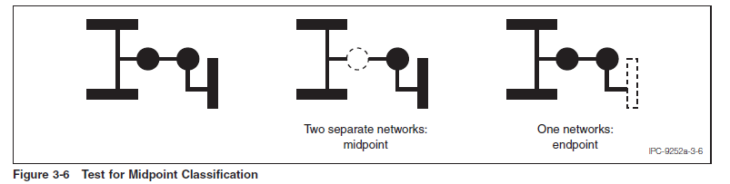 Figure 95: Midpoint classification
Continuity test method
Resistive continuity testing shall be performed on final PCBs using flying probe equipment.
The test voltage shall be maximum 10 VDC.
The current shall be maximum 30 mA.
The resistance threshold shall be maximum 10 Ω in conformance with IPC-9252A class C, except for nets that are designed with high resistance in PCB definition dossier.
- Examples of nest designed with high resistance are planar transformers and coils.
All end points of all nets shall be tested.
The diameter of plated holes and the size of pads shall not be used as a criterion to exclude them from testing. - A pad can be an SMT pad, a circular or oblong pad of a plated hole.
Test point assignment shall be set as follows: - On the top and bottom layer of a drilled pad that is not connected with any track.
- On the top layer of a drilled pad that is not connected with any track on the top layer and connected with only one track on the bottom layer.
- On the bottom layer of a drilled pad that is not connected with any track on the bottom layer and connected with only one track on the opposite layer.
- On the top and bottom layer of a drilled pad that is not connected with any track on the top layer or the opposite layer, but is connected to one inner layer.
- On the bottom layer of a drilled pad that is not connected with any track on the bottom layer and connected with more than one track on the opposite layer.
- On the top layer of a drilled pad that is not connected with any track on the top layer and connected with more than one track on the opposite layer.
- On the top and bottom layer of a drilled pad that is not connected with any track on the top layer or the opposite layer, but is connected to two or more inner layers.
- These 7 conditions for test point assignment are illustrated in Figure 96.
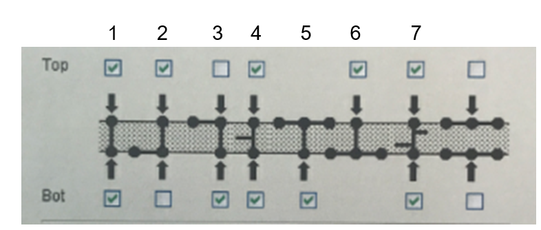 Figure 96: Setting of test point assignments. The numbers 1 to 7 correspond to the conditions of requirement 9.3.8.2g.
During the data preparation, the PCB manufacturer shall verify that end points are included in the test in conformance with requirement 9.3.8.2g.
To fulfil this requirement 9.3.8.2h, it is good practice that the PCB manufacturer defines the PCB data as a “flash”, not as a “contour”, or as a “complex aperture”.
The PCB procurement authority should include in its PCB definition dossier the data preparation for continuity test in conformance with requirements 9.3.8.2g and 9.3.8.2h.
The PCB procurement authority shall specify in the PCB definition dossier in case the continuity test includes text and logo.
Group 2 - Miscellaneous tests
Overview
Long-time overload and short-time overload testing is specified in ECSS-Q-ST-70-10 clauses 7.3.5.1.2 and 7.3.5.1.3. These tests assess the ability of copper tracks and vias to carry a specified current. This test is considered obsolete and covered by the following:
copper foil and copper plating quality is monitored by specifying purity , elongation, layer thickness and its procurement specification,
dielectric quality and thermal robustness is monitored by thermal stress tests and by specifying layer thickness and its procurement specification,
current carrying capacity and self-heating of conductors is specified in PCB design in clause 13.6 of ECSS-Q-ST-70-12.
Internal short circuit testing has been specified in ECSS-Q-ST-70-10 clauses 7.3.5.2. This test assesses leakage current in dielectric insulation between different nets on specific test patterns on coupons. This test is considered obsolete and covered by the following:
High resistance electrical testing on PCBs in conformance with clause 9.3.7.
Water absorption testing is specified as an optional test in ECSS-Q-ST-70-10 clauses 7.3.6.1. This test assesses the weight percentage of water that can be absorbed by the dielectric materials. This test is considered obsolete and covered by the following:
Water absorption is described in the specifications of raw materials, such as IPC-4101E for rigid laminates, IPC-4103A for RF laminates, IPC-4204A for flexible laminates, IPC-4203A for coverlay.
A standard bake-out and prevention of re-absorption are specified for thermal stress tests and assembly.
The effect of water absorption on ECM is assesses by THB and CAF testing in conformance with clause 9.7.
Peel strength
The test shall be carried out in conformance with condition A of test method 2.4.8c from IPC-TM-650.
The conductor selected shall be peeled back at one end for a length of approximately 10 mm.
The detached end of the conductor shall be gripped over its whole width.
Traction shall be applied in a direction perpendicular to the plane of the sample until the copper starts to peel away.
The rate of traction shall be kept constant at 50 mm/minute.
The traction direction shall be kept perpendicular to the plane of the sample.
This can be achieved by positioning the sample on a sliding platform.
Machine inertia shall have no effect on the measurement.
The conductor width shall be the measured width over which the conductor is adhered to the substrate.
Test coupon P from IPC-2221B is an example of a suitable test pattern.
Peel strength of copper foil on laminate or prepreg shall be in conformance with the specification from the datasheet from the raw material manufacturer and from IPC-4101E.
Peel strength shall be determined on representative build-up with either copper foil and prepreg or laminate as external layer.
Peel strength of copper foil 17 µm should be as follows:
- On epoxy: 12 N/cm;
- On polyimide: 12 N/cm;
- On PTFE reinforced/ceramic filled or nonfilled: 8 N/cm;
- Cross-linked hydrocarbon: 8 N/cm;
- Aramide/polyimide: 6 N/cm;
- On flex laminate: 10 N/cm. Peel strength of copper foil 17 µm should be 9 N/cm.
Peel strength below the requirements 9.4.2k and 9.4.2l are evaluated by thermal cycling in qualification.
Flexural fatigue
Flexural fatigue shall be determined only for flexible laminate.
The objective of the flexural fatigue test is to determine the ductility and adhesion of copper cladding, kapton laminate and coverlay.
The flexible sample shall include etching of the pattern and coverlay bonding representative of the PCB.
Flexural fatigue test shall be performed for a flexible PCB.
A flexible PCB can be manufactured using a double sided flex laminate or sculptured copper layer.
Flexural fatigue test shall be performed for a rigid-flex PCB on the individual flexible laminate.
Flexural fatigue test assesses the bare laminate properties. The individual flexible laminate can be non-representative of a rigid-flex PCB in case multiple flexible layers are used or laminated together. In this case, the bending test assesses the representative construction.
Flexural fatigue test shall cover only static applications.
Dynamic applications are project qualified in conformance with requirement 8.6.2b of ECSS-Q-ST-70-12.
The test shall be carried out in conformance with test method 2.4.3.1c of IPC-TM-650 and paragraph 3.10.14 of IPC-6013D.
The equipment can be similar to the automated equipment described in IPC-TM-650 2.4.3.1c. Alternatively the test can be performed using a manual equipment.
The test shall be performed using the following parameters:
- Number of cycles is 250;
- One cycle includes bending the flex laminate upwards 90° and downwards 90°;
- The diameter of the mandrel over which the flex laminate is bend is between 3 mm and 10 mm;
- The rate does not exceed 20 cycles per minute.
For requirement 9.4.3g.3, IPC-TM-650 2.4.3.1c recommends 6,35 mm for single sided flex laminate. ECSS-Q-ST-70-10 clause 7.3.3.3 specifies 9,6 mm. A typical test is performed using 3,2 mm.
Before and after the test, the resistance shall be measured using 4-wire resistance measurement with the sample in flat condition, bend 90° upwards and bend 90° downwards.
The flexural fatigue test shall be performed on two samples manufactured in zero and 90°, covering both orthogonal directions.
This is done to allow T-shaped and L-shaped flex sections. In addition, the raw material CoC can lack the traceability of the processing direction of the copper cladding. A typical flex laminate can use rolled and annealed copper in conformance with requirement 8.3.3d and 8.3.3.e of ECSS-Q-ST-70-12. In this case, the performance of flexural fatigue can be better in the rolled direction than in the other direction. This is caused by the long grain direction of the rolled copper.
The test vehicle shall be microsectioned at the zone that was bend during the test.
The acceptance criteria shall be as follows:
- Resistance change is ≤ 10 %;
- Visual and microscopic inspection is in conformance with clause 10.
- 1 This is done to verify absence of adhesion defects between coverlay and copper, between coverlay and flex laminate and between copper and flex laminate in the bend flexible zone.
- 2 Test coupon X from IPC-2221B is an example of a suitable test pattern.
Bending test
Bending test shall be performed only for rigidflex PCBs.
The objective of the bending test is to determine the adhesion of flex layers and the rigid-to-flex interface.
Bending test shall cover only static applications.
Dynamic applications are project qualified in conformance with requirement 8.6.2b of ECSS-Q-ST-70-12.
The test shall be carried out in conformance with requirements 9.4.3f and 9.4.3g, 9.4.3h, except for the following:
- Number of cycles is 25;
- The radius of the mandrel over which the flexible section is bend equals 12x the total thickness of the flexible section.
The build-up of flex laminate with lowest thickness includes 25 μm flex laminate, with 35 μm copper cladding on both sides, with 25 μm coverlay on both sides, with approximately 10 μm to 20 μm adhesive between coverlay and flex laminate. This results in approximately 165 μm thickness. The minimum bend radius of 12x is in conformance with clause 8.6.2a of ECSS-Q-ST-70-12. The minimum mandrel radius therefore equals 1,98 mm, corresponding to a diameter of 3,96 mm.
The test vehicle shall be the final rigid-flex PCB or a representative coupon.
This is representative of the number of flex laminates, the thickness of flex laminate, thickness of copper cladding, thickness of coverlay, thickness of bond-ply and penetration of coverlay and bond-ply into the rigid section.
The test vehicle shall be microsectioned at the rigid-flex interface and at the zone that was bend during the test.
The acceptance criteria shall be as follows:
- Resistance change is ≤ 10 %.
- Visual and microscopic inspection is in conformance with clause 10.
This is done to verify absence of adhesion defects between coverlay and copper, between coverlay and flex laminate, between copper and flex laminate and between prepreg and coverlay in the rigid-to-flex interface and in the bend flexible zone.
Coating adhesion – tape test
The coating adhesion test shall be performed in conformance with test method 2.4.1e from IPC-TM-650.
Coating adhesion test is performed to determine adhesion of surface finish. Examples of surface finish that can be submitted to this test are SnPb, galvanic Au or Ni-Pd-Au.
After cleaning, an adhesive tape, at least 50 mm long, shall be applied to the test surface and pressed down to eliminate all air bubbles.
After 1 minute, the tape shall be quickly pulled off perpendicular to the coating surface.
The surface area to be tested shall be at least 1 cm2 of conductor.
The tape shall have an adhesion of at least 4,4 N/cm.
Example of tape that can be used is 3M Brand 600 with a width of 13 mm.
The surface finish shall not peel from the test surface or stick to the tape.
Coating adhesion test can be performed on coupon P from IPC-2221B.
Analysis of tin-lead coating
The tin-lead alloy should be chemically dissolved.
The relative quantities of tin and lead should be determined by atomic absorption spectrometry.
This is the preferred method for SnPb.
Another method resulting in the same degree of precision may be used.
The composition of tin-lead shall be: Sn = 63 % ± 8 %
- 1 Lead-rich underplating of tin-lead finish can cause the content of tin in the final reflowed finish to be below the required 55 %.
- 2 Analysis of SnPb coating can be measured coupon P from IPC-2221B.
Outgassing
The outgassing test shall be performed in conformance with ECSS-Q-ST-70-02.
The outgassing test shall be performed on a specimen without copper.
The outgassing shall be determined by measurement of the difference in weight of the specimen before and after the test.
The outgassing shall be:
- RML ≤ 1 %;
- CVCM 0,1 %.
Clauses 5.1.a and 5.5.1.b from ECSS-Q-ST-70-02 specify that a standard outgassing test can be valid for continuous operation of general materials up to 50 °C. However, PCBs are qualified for a maximum operational temperature of 85 °C in conformance with requirement 5.1b of ECSS-Q-ST-70-60. Projects with critical applications can specify more stringent assessment on outgassing in conformance with ECSS-Q-ST-70-02, but this is not covered by generic qualification of PCBs in conformance with ECSS-Q-ST-70-60.
Thermal analysis
Thermal analysis should be performed on a sample without copper.
Temperature of decomposition, Td, shall be measured in conformance with test method 2.4.24.6 of IPC-TM-650 using TGA.
Time to delamination at 288˚C, T288, shall be measured in conformance with test method 2.4.24.1 of IPC-TM-650 using TMA.
Tg should be measured in conformance with test method 2.4.25c of IPC-TM-650 using DSC.
Tg may be measured in conformance with test method 2.4.24c of IPC-TM-650 using TMA.
Tg, T288 and Td are important properties that affect the thermal reliability, especially for assembly operations.
CTE in Z-direction or Z-axis expansion shall be measured in conformance with test method 2.4.24c of IPC-TM-650 using TMA.
CTE in Z-direction is an important property that affects the thermal reliability of a via. “Z-axis expansion” is measured over a wide temperature range of (50-260) °C, which typically generates more reliable test data than “CTE in Z-direction”.
The results of thermal analysis should be verified against the slash sheet of IPC-4101E and the supplier specification of the raw materials.
It is not expected that this verification shows measurements identical to the datasheets. This is performed to obtain reference measurements.
Flammability
Flammability shall be in conformance with ESA-HRE-IPL-RQ-0002 chapter 9.2.3.
Flammability testing should be performed in conformance with ECSS-Q-ST-70-21.
This is important for human spaceflight. Product Assurance and Safety Requirements for ISS Pressurized Payloads ESA-HRE-IPL-RQ-0002 chapter 9.2.3 specifies “All payloads materials shall be assessed for flammability by analysis or test according to the flammability requirements in paragraphs 3.10.2 to 3.10.2.2 of SSP 51700 and JSC 29353.”
Offgassing
Offgassing shall be in conformance with ESA-HRE-IPL-RQ-0002 chapter 9.2.4.
Offgassing testing should be performed in conformance with ECSS-Q-ST-70-29.
This is important for human spaceflight. Product Assurance and Safety Requirements for ISS Pressurized Payloads ESA-HRE-IPL-RQ-0002 chapter 9.2.4 specifies “Determination of offgassing products from materials and assembled articles shall meet the offgassing acceptance criteria in paragraph 7.7.3 of NASA-STD-6001B.”
Solderability
Overview
The objective of the test is to verify the wettability on PTH. This is performed by floating a sample on molten solder and by assessing the rise of the solder in the PTH. Coverage of solder on the corner of a PTH is more difficult to achieve uniformly compared to an SMT pad. When the solderability test passes on PTH, it is, therefore, also expected to pass on SMT pads. Thus, the need for solderability test on SMT pads has not been identified if it is already performed on PTH.
Test vehicle
The test pattern for solderability test shall be one of the following:
- Coupon A/B with PTH as specified in requirement 8.2.2d, or
- PCB sample with PTH. The coupon shall include representative PTH in accordance with ECSS-Q-ST-70-12 requirements 15.2d.2, 15.2d.4, 15.2d.5(a) and 15.2d.8.
- 1 Requirements 15.2d.2 and 15.2d.4 specify to include a representative configuration of copper planes and internal heat sink. Requirements 15.2d.5(a) and 15.2d.8 specify to include PTH with hole sizes of maximum or most frequently used dimensions.
- 2 Solderability coupon type “S” from IPC-2221B specifies dimensional parameters and need to be tailored to meet requirement b.
The coupon shall include minimum three PTH.
Solderability test parameters
The solder shall be type “63 tin solder” in conformance with table 6-1 of ECSS-Q-ST-70-08.
The flux shall be type “ROL0” in conformance with table 6-2 of ECSS-Q-ST-70-08.
The solder bath shall be temperature controlled in conformance with clause 7.2.3.2.2 for pretinning of ECSS-Q-ST-70-08.
The tolerance of the temperature control of the solder bath shall be ±5°C.
The solder bath temperature shall be set at 235°C.
Test flow
After sampling the coupon, it shall be cleaned using a cleaning agent in accordance with clause 6.4 of ECSS-Q-ST-70-08.
Bake-out is not mandatory. Bake-out can slightly increase the intermetallic layer. This effect is minor compared to the pre-conditioning.
Pre-conditioning of the sample should be performed by applying a heating profile to the coupon in conformance with IPC-TM-650 2.6.27 that is representative of vapour phase reflow.
- 1 This pre-conditioning method can be simulated by 2 X 5 minutes at 230°C in an oven, which is in accordance with Table 4-2 of IPC-J-STD-003C. The oven is set at and pre-heated to 230°C. The timing of 5 minutes is in between door openings. A forced air convection oven provides the best transfer of heat to the sample.
- 2 The purpose of pre-conditioning is to simulate the vapour phase reflow that can occur on both sides of a PCB with SMT components prior to soldering of PTH. However, this preconditioning is not a mandatory part of the test flow because it is difficult to perform in a representative manner and because historically customers have not reported poor solderability on SnPb surface finish.
Flux shall be applied to the test area and drained on absorbent, clean material prior to solderability test.
The solderability test shall be performed in not less than one minute, and not more than five minutes after application of flux.
Dross and burned, residual flux shall be removed from the surface of the molten solder immediately prior to solderability test.
Solderability test shall be performed by floating the coupon on molten solder for a maximum duration of 30 s.
During solderability test, the coupon may be depressed into the solder bath to a maximum of 50 % of the coupon thickness.
* This solderability test is in conformance with paragraph 4.4.1 of IPC-J-STD-003C.
After the elapsed time, the coupon shall be removed from the molten solder and maintained still and horizontal until the solder on the coupon solidifies.
Prior to examination, all specimens shall have the flux removed using a cleaning agent in accordance with clause 6.4 of ECSS-Q-ST-70-08.
Test specimens shall be examined at 10X magnification by visual inspection on the side that was not in contact with the solder.
Microsectioning is not needed.
Acceptance criteria
Acceptance criteria for solderability of PTH shall be as specified in Table 91.
- 1 The wetted corner on ≥25% of the circumference is specified for a component lead in requirement 10.3.3.2a of ECSS-Q-ST-70-08.
- 2 The nonconformance criteria are based on visual inspection. The schematic drawings of cross-sections are only shown for illustration and information. The wetting angle is not evaluated in this test.
- 3 In case of unacceptable solderability in conformance with this test method, it is good practice to further investigate by soldering a wire in conformance with ECSS-Q-ST-70-08.
Table 91: Nonconformance criteria for solderability of PTH
|
Schematic cross-section(for information)
|
Nonconformance criteria based on visual inspection
|
Evaluation
|
|
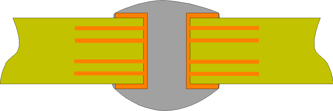
|
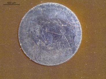
|
Acceptable if:
|
|
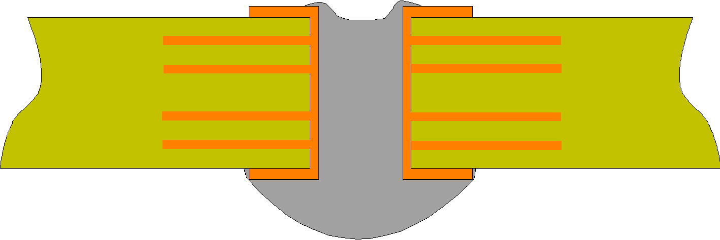
|
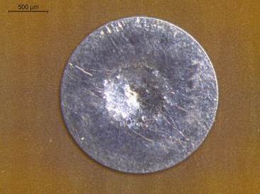
|
|
|

|
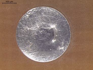
|
Acceptable if:
|
|

|
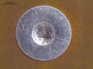
|
Not acceptable if:
|
Group 3 – Thermal stress and as-received
Overview
The solder bath test is a quick and easy test method to assess robustness of the sample under thermal stress.
Rework simulation is performed to simulate the thermal stress caused by hand solder assembly, rework and repair. The quality of the solder joint is not assessed. This test method can be tailored to be performed on SMT pads.
The rework simulation test method specifies 10 heat cycles. However, worst-case assembly, rework and repair can include more than 10 heat cycles. The stress specified by the test method covers a typical assembly process, but it does not cover worst-case. In case it is foreseen to exceed these test conditions, it is good practice to perform a specific evaluation.
A sample for rework simulation typically includes other holes for evaluation as-received.
Microsectioning
Method
The methods for microsectioning from test method 2.1.1f from IPC-TM-650 should be used.
Sampling
The sampling method shall not damage the area of interest to be inspected in the microsection.
For instance, milling or sawing can cause vibrations that can cause delamination. This is especially important for the rigid-to-flex interface. It is good practice to saw far away from the plane of interest and to grind to the plane of interest once the sample is potted.
Potting
Samples and cups for potting shall be clean.
Cleaning can be done ultrasonically with isopropanol.
Potting of the sample with resin shall provide edge retention.
Edge retention is achieved by using a hard resin, such as epoxy. However, also some acrylic resins can achieve good results. Acrylic resins can be preferred in an industrial environment above epoxy ones because of the faster curing time.
The potting should be free from air bubbles.
Absence of air bubbles can be achieved by submitting the uncured potted microsection to a vacuum or overpressure.
The curing of the potting resin shall not generate heat that cause damage to the sample.
The mixing time and ratio of the resin as specified by the supplier shall be followed.
Fluorescent dye should be used for potting of the rigid-to-flex interface.
In case fluorescent dye is not used for potting of rigid-to-flex interface, the following shall be demonstrated:
- the efficiency to detect possible delamination without the contrast from the fluorescent dye;
- any possible delamination is not caused by the microsectioning.
Surface preparation
The quality of as-polished microsections shall be free of scratches.
Examples of microsectioning and microscopy showing target quality are shown in Figure 97.
The quality of grinding and polishing of microsection shall prevent smearing of soft materials, such as copper.
- 1� Smearing of copper can cover interface lines that can be indicative of adhesion defects, such as interconnect defect.
- 2 It is good practice to perform grinding with incremental grit, for instance 180, 320, 800, 1200, 2500.
- 3 It is good practice to perform polishing with decremental polishing paste size, for example:
- 6 μm polish pad and diamant paste, 20N, 150 rpm, 120 sec;
- 3 μm polish pad and diamant paste, 20N, 150 rpm, 90 sec;
- 1 μm polish pad and diamant paste, 20N, 150 rpm, 60 sec;
- 0,25 μm polish pad and diamant paste, 20N, 150 rpm, 45 sec.
Micro-etching of microsections shall be sufficient to reveal interfaces between plating steps. - 1 Adhesion defects are investigated on as-polished microsections, without the use of micro-etching. This is because micro-etching always causes an interface line to become visible between different copper plating steps. After a defect has been identified, it is useful to micro-etch the microsection to investigate at which plating interface the defect is observed. If potential nonconformances are observed, a polish-etch-polish process can provide a more detailed investigation method.
- 2 An adequate etching can be achieved, for example, by submerging the sample for 5 to 10 seconds in a solution of 25 ml demineralised water, 25 ml ammonia solution 25 % and 1 ml hydrogen peroxide solution 30 %.
The plane of the microsection should be in the centre of the hole. - 1 This is especially important for dimensional measurements.
- 2 This is described in clause 3.6.1.5 of IPC-6012D and test method 2.1.1f from IPC-TM-650.
Microscopy
Quality of metallisation shall be inspected in bright field.
Bright field achieves the best contrast in the metallised areas.
Quality of laminate shall be inspected in dark field or an equivalent lighting method.
- 1� Dark field uses a high illumination intensity showing features underneath the surface of the microsection by transparency of the resin. A similar high illumination intensity can be obtained using polarisation filters.
- 2 Subsurface cracks in laminate can be visible as an area showing “iridescence” in dark field. To conclude on the nature of the iridescence it is good practice to perform progressive polishing to have the surface of the microsection at the same level of the feature. In this case a crack shows up in bright field since it is in the surface of the microsection.
The magnification for microscopic inspection may be 50x to 1000x.
The specific magnification for microscopic inspection for each acceptance criteria shall be as specified in clause 10.
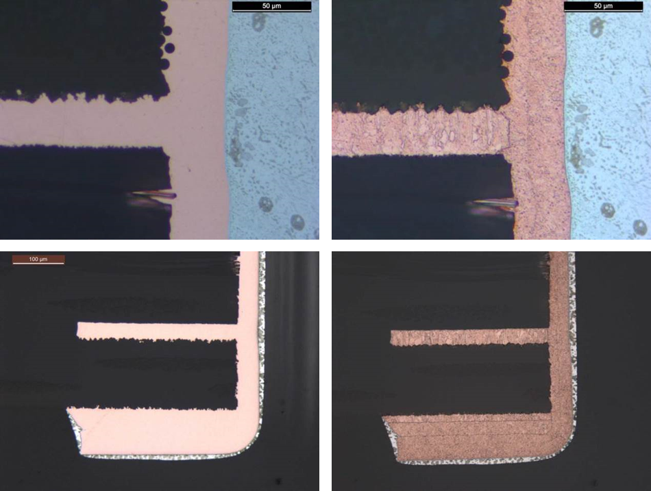 Figure 97: Example of target quality of microsection of innerlayer (top) and knee of the hole (bottom), as-polished (left) and after micro-etch (right).
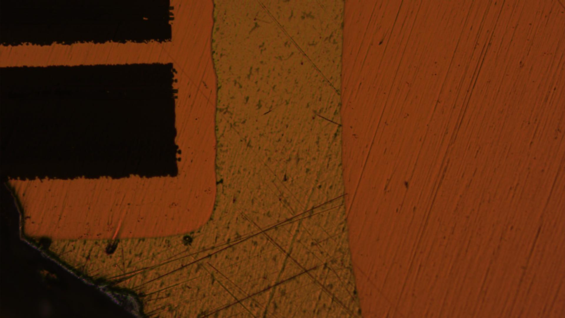
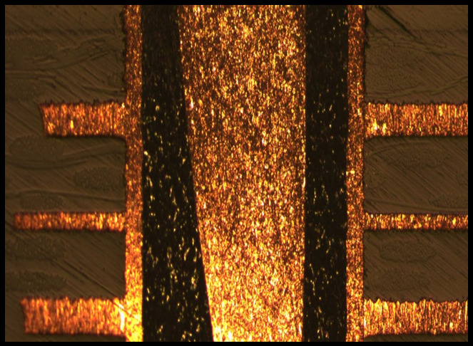
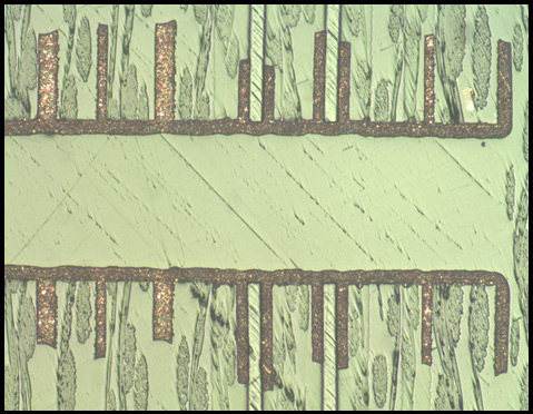 Figure 98: Examples of inadequate quality of microsection showing in the top image inadequate polishing, leaving scratches on surface, in the middle image over-etched sample and in the bottom image inadequate lighting, revealing no detail on metallisation, nor on laminate by transparency.
Solder bath float
The test shall be carried out in conformance with condition A of test method 2.6.8e of IPC-TM-650.
Samples shall be baked in conformance with clause 9.2.2.
The solder bath float shall be performed to one side of the sample by floating it for 10 s in a solder bath maintained at 288 C.
The sample shall be removed from the bath and cooled down to ambient conditions for a duration of at least 2 minutes.
The solder bath float and cool down from requirements 9.5.3c and 9.5.3d shall be performed 3 times in total.
The acronym for the solder bath floating test is “SB”. This acronym refers to this test method which specifies 3 cycles. Thus, “SB” does not imply only 1 heat cycle.
The samples shall be inspected to ensure that holes are wetted.
The samples shall be inspected to evaluate the visual aspects of the substrate in conformance with clause 10.4.
The samples shall be microsectioned for evaluation of qualitative aspects in conformance with clause 10.3.
Rework simulation
Test vehicle
The test pattern for rework simulation test shall be one of the following:
- Coupon A/B with PTH as specified in requirement 8.2.2d, or
- PCB sample with PTH. The coupon shall include representative PTH in accordance with ECSS-Q-ST-70-12 requirements 15.2d.5(a) and 15.2d.8.
These clauses specify to include PTH with hole sizes of maximum or most frequently used dimensions.
Rework simulation test parameters
The solder shall be type “63 tin solder” in conformance with table 6-1 of ECSS-Q-ST-70-08.
The flux should be type “ROL0” in conformance with table 6-2 of ECSS-Q-ST-70-08.
The solder iron and solder tip shall in conformance with clause 5.6.7 of ECSS-Q-ST-70-08.
To meet requirement 5.6.7e. of ECSS-Q-ST-70-08 it is good practice to use a solder iron with a power of ≥ 80 W.
The solder tip temperature shall be set at 350 °C.
This temperature covers the maximum temperature in conformance with requirement 5.6.7h of ECSS-Q-ST-70-08 for epoxy and polyimide technology without large thermal mass. For polyimide technology with thermal mass, requirement 5.6.7j of ECSS-Q-ST-70-08 allows a higher soldering temperature of 380 °C. This is not covered by the rework simulation test using the specified conditions.
Test flow
Bake-out of the sample shall be performed in conformance with the clause 9.2.2.
Copper wires should have a diameter of 0,2 mm to 0,7 mm smaller than the diameter of the PTH.
Copper wires may be solid wire or stranded wire.
The wire and PTH shall be fluxed.
The wire shall be pretinned.
The wire shall be inserted in the PTH and soldered.
Rework can be performed on SMT pads for specific technology as specified in requirement 9.8.2h.
During soldering the tip of the solder iron shall be in contact with the pad of the PTH and the wire for a maximum duration of 5 seconds.
Sample with high thermal mass should be submitted to pre-heating during the rework simulation test.
This is done to limit the soldering time to maximum 5 seconds.
After soldering, the sample shall be allowed to cool down for at least 30 s.
Additional flux shall be applied after the cool down, just prior to the next solder cycle.
While the solder is molten in conformance with requirement 9.5.4.3g, the wire shall be moved by at least 5 mm.
It is good practice not to remove the wire from the PTH and not to re-insert during subsequent solder cycle. This is done to avoid mechanical stress, which is considered to be less reproducible and dependant on operator and dimensions of wire and PTH. The test method is intended to impose thermal stress only. However, removal of wire can be optionally performed but this only provides a conclusive outcome if results are positive.
Clauses 9.5.4.3i, 9.5.4.3j and 9.5.4.3k shall be repeated 10 times in total.
- 1 The wire is left inside the PTH.
- 2 The acronym for the rework simulation is “RW”. This acronym refers to this test method which specifies 10 cycles. Thus, “RW” does not imply only 1 heat cycle.
- 3 The worst-case combination of initial assembly, maximum number of repairs and maximum number of rework per component assembly can include a number of heat cycles that is higher than the 10 specified in this test method.
A microsection shall be performed on the soldered hole including the wire to evaluate the qualitative aspects in conformance with clause 10.3.
Interconnect stress test (IST)
Overview
IST testing is a test method that performs rapid thermal cycling on IST coupons. The IST coupons are daisy-chained vias with power circuits through which a current is applied to heat the IST coupon and sense circuits that are used to monitor the resistance change as function of thermal cycling.
PCB technology of highest complexity or with aspects that are expected to affect thermal endurance are IST tested within the technology perimeter for procurement as specified in 9.5.5.2.2. In addition, in-process IST testing as well IST testing for qualification is performed. The thermal endurance of PCB technology that does not fall within the technology perimeter as specified in 9.5.5.2.2 is, therefore, covered by the in-process IST verification.
Technology perimeter
In-process control
The PCB manufacturer shall have a work instruction for in-process IST control.
In-process IST control shall enable quantification of the reliability and monitoring of the stability.
The PCB manufacturer shall specify the IST coupon design and IST test method to be used.
This can deviate from the IST test parameters from clause 9.5.5.4.
The work instruction for in-process IST control shall specify the following:
- The technology, build-up and design reference of the IST coupon;
- The rationale for the IST coupon design based on the PID;
- IST test parameters;
- Test moment and frequency;
- Statistical Process Control (SPC) limits.
A typical frequency of testing is once per week or two weeks.
Procurement
IST shall be performed for procurement in case the PCB definition dossier includes one or more of the following:
- Any PCB with ≥ 0,3 mm in Z-direction as-designed insulation distance of no-flow prepreg or 85NT;
- Epoxy PCB with ≥ 12 copper layers;
- Rigid-flex PCB with one or more of the following aspects:
- ≥ 12 copper layers, or
- ≥ 2 flex laminates, or
- asymmetric build-up or asymmetric lamination;
- HDI PCB with microvias or with aspect ratio > 7.
- 1 No-flow prepreg and 85NT have high thermal expansion in Z-direction. The thermal expansion is the driver for barrel crack and therefore necessitates IST testing.
- 2 See Table B-6 for an example of a build-up report with as-designed insulation distance.
At least one coupon shall be included per panel and submitted to IST testing.
Qualification
IST shall be performed for qualification activities in conformance with clause 7.2.
IST shall be performed until 5 % resistance increase is reached or until a maximum of 1500 cycles.
- 1 Acceptance criteria are as per clause 9.5.5.4.3. Testing to EOL is performed to provide information about the limits of the robustness.
- 2 At least 3 IST coupons are used for initial qualification and at least 1 IST coupon is used for delta qualification and qualification renewal, in conformance with clause 5.7.
- 3 For qualification it is not practical to test microvias after having tested other via types on that coupon to EOL.
IST coupon design and location on panel
The IST coupon design shall be type “X”.
- 1 For instance “TVX” or “SLX”. This indicates the presence of an internal (‘P’) and external (‘H’) heating circuit.
- 2 An IST coupon typically includes two power circuits (H and P) and two sense circuits (S1 and S2). One sense circuit can include more than one plating sequence. In some cases more than one IST coupon is needed to represent all vias and plating sequences.
- 3 The sense circuit is typically designed to be sensitive to barrel crack. The power circuit applies heat to the coupon and in addition it is typically designed to be sensitive to interconnect defect. The standard power circuit is applied through interconnects on 4 internal layers. Therefore these are assessed by IST, whilst other layers remain unassessed. In case the need arises for more comprehensive assessment of interconnections of all layers, PWB Corp can be requested to design specific coupons.
IST coupon design shall be representative of the PCB for the following features: - minimum drill diameter;
- minimum drill pitch for the via type;
- all plating sequences, except for the case 9.5.5.3c;
- pad diameter;
- copper foil thickness;
- presence of non-functional pads;
- layer function for signal or plane;
- diameter of clearance holes in planes.
- 1 An IST coupon design work sheet is available on the test equipment supplier’s website www.pwbcorp.com that includes these items.
- 2 Space PCBs typically use SnPb surface finish. During IST testing it has been observed that SnPb enters into barrel cracks and crack initiations. This can accelerate crack growth due to wedging. This can also mask or delay resistance increase. Therefore SnPb finish can be stripped and bare copper coupons can be tested. Studies have shown correlation between both configurations.
- 3 Multiple coupons can be necessary to accommodate IST on all plating sequences.
- 4 The procurement authority is accountable for the design of the IST coupon in conformance with requirement 15.1a. from ECSS-Q-ST-70-12.
The plating sequence to manufacture a buried via across top and bottom layer of a single laminate need not to be included in the IST coupon.
The coupon should be located as close as possible to the PCB.
In case of more PCBs per panel, the coupon should be located as close as possible near the centre of the panel.
The coupon should not be located in the corner of the panel.
This is done to be representative of worst-case Cu coverage. Location of IST coupon on the panel is shown in Figure 83.
IST test method
Preparation
Electrical pre-screening and possible down selection should be performed in conformance with instruction PWB-150316 in case multiple IST coupons are available.
The referenced work instruction is available on the website of the test equipment supplier.
Bake-out of IST coupons shall be performed in conformance with requirement 9.2.2a.
After bake-out, connectors shall be soldered to the IST coupon.
Reabsorption of humidity in IST coupons should be prevented in conformance with requirement 9.2.2d.
Correct soldering of connectors should be verified by measuring again the resistance of IST coupons.
In uncontrolled conditions, IST coupons shall be submitted to IST testing within 12 hours after baking.
In case re-absorption of humidity is mitigated in conformance with point 9.5.5.4.1d, IST coupons need not to be submitted to IST testing within 12 hours after baking.
IST test parameters
IST shall be performed in conformance with test method 2.6.26A from IPC-TM-650, except for the parameters specified in this clause 9.5.5.4.2.
The IST preconditioning cycles shall be 6 times to 230 °C, except for the case specified in 9.5.5.4.2c.
The IST preconditioning cycles may be tailored in case all the following conditions are met:
- The IST preconditioning cycles are representative of the assembly environment and potential repair and rework;
- The IST preconditioning cycles are minimum 3 times to 230 °C.
Preconditioning parameters specified in this clause are representative of the assembly environment, which typically uses tin-lead solder. In case of lead-free assembly, it is expected that the preconditioning is increased to 245-260 °C and this can have significant impact on IST endurance.
The power circuit for preconditioning shall be the “superheat” circuit
Superheat circuit is identified by “H”.
IST cycling shall be performed to the following temperature limits:
- polyimide: 170 °C;
- epoxy: 150 °C;
- microvias on polyimide: 210 °C;
- microvias on epoxy: 190 °C. Failure threshold of resistance change shall be 5 % for standard holes.
In case a resistance below 250 mΩ is measured during electrical pre-screening, in conformance with 9.5.5.4.1a, the noise can be high. In this case it is good practice to confirm the failure threshold with the test equipment supplier. This can result in re-design of the coupon for future use.
Failure threshold of resistance change shall be 4 % for microvias.
The failure threshold for resistance change shall apply to all circuits on the IST coupon.
- 1 A failure on the internal power circuit indicates a weak interconnection. This is not the typical failure mode in an IST test. This can cause local over-temperature due to high resistance.
- 2 A failure on the sense circuit indicates barrel crack. This is the typical failure mode in an IST test. This does not cause local over-temperature because this circuit is passive.
“Compensation” shall be “Calculated” for standard tests.
“Compensation” shall be “None” for microvia testing and for testing standard vias with a pitch of ≥ 2,5 mm.
“Sense Fail Type” shall be “A or B”.
The power circuit for IST cycling shall be the internal power circuit. - 1 The internal power circuit is identified by “P”.
- 2 IST cycling includes the first few IST cycles before preconditioning and all IST cycles after preconditioning.
For testing microvias, the power cable shall be connected directly to the microvias sense circuit.
The sense cable is connected to a power or sense circuit that has previously demonstrated to be robust, e.g. the superheat circuit. The measured sense data is not considered important and any failure or variation measured is disregarded.
IST acceptance criteria
Any coupon shall have an IST endurance of ≥ 400 cycles for standard holes.
Any coupon shall have an IST endurance of ≥ 100 cycles for microvias.
Any coupon should have an IST endurance of ≥ 400 cycles for microvias.
- 1 IST testing of microvias can be performed after IST testing of standard holes in case both hole types are present on the same coupon. The IST cycles for standard holes occur to a lower temperature, which does not impact the IST performance of the microvia circuit tested subsequently.
- 2 Microvias are expected to withstand 400 cycles as per requirement 9.5.5.4.3c, analogous to other via types. Microvias are expected to fail within the first 100 cycles, or not at all. Therefore, a test protocol is specified only until 100 cycles, which has heritage for the IST equipment supplier. It is good practice to test until 400 cycles occasionally, for instance for qualification.
Analysis and reporting
After IST testing, the coupon should be submitted to microsectioning.
In case the required number of IST cycles are not achieved, the coupon shall be submitted to microsectioning to investigate the cause of failure and possible corrective actions.
The location for microsectioning should be determined by observing the hotspot during infrared thermography while a small current is passed through the failed circuit.
- 1 The purpose is to get a visual confirmation of the failure mechanism in the metallisation. Barrel crack, wear-out of the copper barrel and innerlayer separation should be the main focus of this inspection.
- 2 In case tin-lead is included on the IST coupon, it is good practice to verify the absence of tin-lead in barrel cracks by microsectioning, as this can impact the measured IST endurance. An example of this is shown in Figure 99.
The IST test report shall include the following: - Summary of test parameters;
- Reference to the coupon design drawing;
- Graph of resistance change as function of IST cycles.
 Figure 99: Examples of barrel cracks after IST testing showing a nominal crack size (left) and a large crack filled with SnPb (right)
Special IST test for RF PCB technology
Overview
Standard IST coupon design includes interconnects on L2+3 (and Ln1 and Ln2) in the power circuit. The sense circuit is designed to be sensitive for barrel crack, as it includes no innerlayer connections. For special technology, this design can be modified to have better sensitivity for interconnects on critical layers. This is of value in case laminate materials are used that are prone to smear, such as PTFE based materials for RF PCBs. Smear can be impacted by drill size and drill bit quality.
IST coupon design for interconnect verification in RF PCBs
Standard IST coupons shall be included for RF PCB in case this is within the technology perimeter in conformance with 9.5.5.2.2a.
Standard IST coupons evaluate mainly barrel strength.
Specific IST coupons for interconnect verification may be included for RF PCB technology to assess smear.
Specific IST coupons for interconnect verification should include all drill sizes for holes that interconnect on RF laminate.
This does not include non-functional pads.
The daisy-chain should include the largest drill diameter for holes that interconnect on RF laminates.
Interconnection in large holes are most stressed during IST cycling.
The daisy-chain should include interconnection on all RF innerlayers.
The daisy-chain should include interconnection on outermost RF innerlayers.
- 1 This is for example L2, L3, Ln-1 and Ln-2.
- 2 The interconnects on outermost innerlayers are most stressed during IST cycling.
The power cable should be connected to the superheat circuit.
This circuit is not affected by the quality of interconnects and provides a stable heat source.
The IST cycling may be performed to a temperature of 210 °C.
The high temperature is used to provide sufficient stress to the interconnections on thermally robust PTFE layers. The possible presence of low Tg laminate needs to be evaluated, but is not deemed critical to this test temperature as sensitivity to barrel strength is designed to be low.
Group 4 – Assembly and life test - extended
Overview
ECSS-Q-ST-70-10 group 4 included thermal cycling. This is superseded by the accumulative test flows of group 4 and group 6 described in this clause and in clause 9.8.
Group 4 includes a higher number of 500 thermal cycles with a lower temperature range of 155 C. In addition, group 4 includes electrical testing and peel strength. The group 4 is performed for initial qualification of a material or technology and provides evidence that the PCB technology withstands the thermal excursions from assembly verification, in conformance with requirement 13.3d of ECSS-Q-ST-70-08 and 14.6 of ECSS-Q-ST-70-38. See clause 9.8.1 for an overview of group 6.
Test flow for group 4
The test vehicle for group 4 shall include the PCB.
The test vehicle for group 4 shall include coupons that are specified for each test method.
The following test steps shall be performed for group 4 in this order:
- bake-out in conformance with clause 9.2.2;
- intralayer and interlayer insulation resistance with DC voltage in conformance with clause 9.6.3;
- intralayer and interlayer dielectric withstanding voltage with DC voltage in conformance with clause 9.6.4;
- reflow simulation in conformance with clause 9.8.3;
- rework simulation on at least 4 PTH of the PCB in conformance with clause 9.5.4;
- thermal cycling in conformance with clause 9.8.4 with the following modifications:
- for requirement 9.8.4g the minimum temperature is -55 C;
- for requirement 9.8.4h the maximum temperature is +100 C;
- for requirement 9.8.4i the temperature range is 155 C;
- for requirement 9.8.4j the number of thermal cycles is 500;
- intralayer and interlayer insulation resistance with DC voltage in conformance with clause 9.6.3;
- intralayer and interlayer dielectric withstanding voltage with DC voltage in conformance with clause 9.6.4;
- peel test in conformance with clause 9.4.1;
- microsectioning in conformance with clause 9.5.2;
- evaluation of acceptance criteria in conformance with clause 10. Microsectioning and evaluation in conformance with 9.6.2c.10 and 9.6.2c.11 shall be performed on the following:
- At least 4 PTH from the PCB that have been subjected to rework simulation;
- All technology features under qualification.
Technology features under qualification can include all via types, the build-up and materials.
Interconnection resistance on a daisy-chain coupon may be monitored during thermal cycling.
In case a daisy-chain coupon is used in conformance with requirement 9.6.2e, change of interconnection resistance shall be ≤ 10 %.
The daisy-chain coupon may be an IST coupon.
- 1 Continuous in-situ measurement using four-wire resistance is commonly performed on coupons in a thermal cycling chamber. The daisy-chain is designed with sufficient length to allow a sensitive measurement.
- 2 This evaluation can provide correlation of traditional chamber thermal cycling with IST cycling by continuous measurement of interconnection resistance on the same pattern. It can also quantify the electrical performance of a thermally stressed daisy-chain by measuring before and after the group 4 test flow.
- 3 Rework simulation is only performed on the PCB. It is not performed on coupons for insulation resistance, dielectric withstanding voltage, IST or peel strength.
Insulation resistance
The insulation resistance test shall be performed in conformance with tests 6a for external intralayer insulation resistance, test 6b for internal intralayer insulation resistance and test 6c for interlayer insulation resistance of IEC 60326-2-am 1 (1992-06).
This test is superseded by the high resistance electrical test on PCB. However, insulation resistance is still measured on coupons before and after environmental testing.
A direct voltage of 250 V shall be applied between the two closest conductors that are not electrically connected.
Table 13-3 and Table 13-4 of ECSS-Q-ST-70-12 allow, for instance, a minimum conductor spacing of 200 µm on external layers without conformal coating, 81 µm on internal layers for HDI and 25 µm between layers on flex laminate.
Test voltage shall be DC for qualification activities.
The procurement authority may define in the PCB definition dossier specific AC insulation resistance testing on coupons or PCB.
- 1 The majority of applications for space are in DC. It is important to note that DC/DC converters can have some AC sections.
- 2 Peak transient voltages in AC or DC is covered by requirement 13.8.2b. from ECSS-Q-ST-70-12.
- 3 The failure mechanisms of primary concern in PCB materials are of slow time constant, such as ECM. In this case, DC is deemed worse-case than AC.
When the voltage is applied, the insulation resistance (R) shall be measured after 1 minute, except the case specified in 9.6.3f.
In case a stable reading is obtained earlier, the insulation resistance (R) may be measured before 1 minute.
The test pattern for intralayer insulation resistance shall have at least 25 mm parallel conductors.
Insulation distance between tracks or between layers is representative of the PCB, as specified in clause 15.2a of ECSS-Q-ST-70-12.
The test pattern for interlayer insulation resistance shall have at least 1 cm2 superimposed conductors.
Test coupon E of IPC-2221B can be used for intralayer insulation resistance. For interlayer insulation resistance, test coupon E is modified as per requirement 9.6.3h.
The intralayer insulation resistance as received shall be ≥ 10 GΩ.
The interlayer insulation resistance as received shall be ≥ 100 GΩ.
The intralayer insulation resistance after thermal stress shall be ≥ 1 GΩ.
The interlayer insulation resistance after thermal stress shall be ≥ 10 GΩ.
To measure such high resistance it is good practice to use an equipment with a measurement range up to 1000 GΩ.
Dielectric withstanding voltage (DWV)
The test shall be carried out in conformance with IPC-6012D chapter 3.8.1 and condition B of test method 2.5.7d of IPC-TM-650.
- 1 This method specifies 1000 V DC for 30 s. The procurement authority can define specific AC testing on coupons or PCB as specified in requirement 9.6.3d.
- 2 PCB qualification does not cover for continuous operation of the assembled PCB at any voltage, which is typically performed at unit level. Bare PCBs are not subject to tests and requirements for rating and derating.
For interlayer measurements the test voltage shall be applied between two superimposed conductors with a surface area of ≥ 1 cm2.
For intralayer measurements the test voltage shall be applied between two adjoining, but not electrically connected conductors within the same layer with a total length of ≥ 25 mm.
Insulation distance between tracks or between layers is representative of the PCB, as specified in clause 15.2 of ECSS-Q-ST-70-12.
Visual inspection shall show no evidence of breakdown, flashover or sparking.
- 1 Test coupon E of IPC-2221B can be used for intralayer DWV. For interlayer DWV, test coupon E is modified as per requirement 9.6.4b.
- 2 Advanced test equipment are capable to monitor voltage or leakage current continuously during the applied test voltage. A sudden drop in voltage is indicative of a discharge. This is relevant because visual inspection is not fully efficient on internal layers covered by plane layers.
Group 5 – ECM tests
Overview
Group 5 in ECSS-Q-ST-70-10 included a damp heat test. This is superseded by the THB and CAF tests specified in this clause.
The THB test has the objective to assess the cleanliness of the sample, which includes cleanliness of raw laminate and cleanliness of PCB manufacturing processes. The adhesion of resin to, for instance, fibre contamination can be degraded during thermal stress of assembly, such as vapour phase reflow. Fibre contamination can provide a pathway for ECM. Because of the relatively large particle size of typical contamination, this type of ECM is possible for PCB designs using standard insulation distance.
The CAF test has the objective to assess the material properties for its CAF resistance. The adhesion of resin to glass fibre reinforcement can be degraded during thermal stress. The glass-to-resin interface, or a hollow glass fibre, can provide a pathway for ECM. The CAF mechanism is only probable at small insulation distance, as for HDI designs. The CAF test can also detect contamination as for the THB test, but this is not its objective.
The environment of THB and CAF tests include a temperature of 85 ˚C because this is the maximum operational temperature for which PCBs are qualified in conformance with requirement 5.1b. The tests include a relative humidity of 75% RH because this provides some margin and acceleration of test compared to the maximum relative humidity of 65 % in clean rooms. However, it is possible that PCB assemblies are tested or operated at higher humidity outside of cleanrooms.
Ground-based testing at unit level is deemed the worst-case environment for a potential ECM because of the presence of humidity in the atmosphere. However, studies have shown that the time constant of desorption of humidity from the somewhat hygroscopic laminate can be underestimated significantly in the presence of ground-planes and other complex PCB geometry.
Temperature, Humidity, Bias (THB)
General
A justification shall be provided in case any part of this test method is tailored.
The specified method can be superseded by future test campaigns to implement lessons learned or to represent applications.
Test vehicle
The lay-out of the test vehicle for THB test shall meet all the following conditions:
- It includes two comb patterns in X and Y-direction on each internal layer;
- It includes 150 μm as-designed insulation distance D between tracks;
- Each comb pattern covers an area of ≥ 30x30 mm;
- The sensitivity of the pattern is ≥ 20000 number of squares.
- 1 An example of a test vehicle for THB testing is shown in Figure 910.
- 2 150 μm as-designed can result in minimum 120 μm as-manufactured.
The sensitivity S of the pattern shall be calculated using the following formula:
Equation Where:
Equation L: length of track
Equation N: number of gaps between tracks
Equation D: insulation distance
- 1 The unit of the sensitivity is “number of squares”. This is a dimensionless value representing the interface area, that is proportional to the sum of the length of parallel tracks and inverse proportional to the insulation distance.
- 2 The pattern in Figure 910 uses 150 μm track width and 150 μm insulation distance over an area of 30 mm length and width. This results in 30/(0,15+0,15)=100 gaps N. Therefore the sensitivity S= 30 x 100 / 0,15 = 20000 number of squares.
The THB test shall assess internal layers.
The build-up of the test sample shall include ≥ 8 copper layers, uni-flow prepreg, no-flow prepreg, flex laminate and rigid laminate materials in conformance with the PID.
An example of the build-up is shown in Figure 911.
The thickness shall be 1,6 mm ± 10 % over connector metallisation.
The manufacture of samples shall follow the process flow as specified in the PID including the manufacture of windows in no-flow prepreg as for rigid-flex PCBs.
Manufacture of windows and use of various materials are sources of contamination which are aimed to be included in the test vehicle.
Copper foil thickness shall be 35 μm.
Surface finish on connector shall not be SnPb
This is specified because SnPb can contaminate the connector pins on the test rack. Alternative finishes, such as galvanic Au and/or Ni or ENEPIG do not show this problem. External layers and surface finish is not within the scope of the test method.
In total four samples shall be tested from at least two different panels.
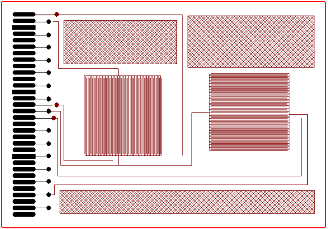 Figure 910: THB test pattern
 Figure 911: Build-up for THB test vehicle
Test method
The sample preparation method shall be as follows:
- bake-out in conformance with clause 9.2.2;
- two times reflow simulation in conformance with clause 9.8.3;
- ultrasonic cleaning followed by bake-out in conformance with clause 9.2.2.
- 1 Reflow simulation is performed to represent assembly environment and because the high temperature can carbonise contaminants or can weaken the adhesion between resin and contaminant.
- 2 Ultrasonic cleaning can be performed in IPA. This is done to ensure clean surfaces in the connector pattern.
The THB method shall be as follows: - THB Ambient using the parameters: 24h, 25°C, 50% RH, 50V;
- THB ECM using the parameters: 150h, 85°C, 75% RH, 50V;
- THB Ambient using the parameters: 24h, 25°C, 50% RH, 50V.
- 1 The THB Ambient part is done to determine ambient insulation resistance prior to and after the THB ECM part. This verifies that any failures during the THB ECM part persist after returning to ambient conditions.
- 2 It is good practice to verify that changes in the environmental chamber do not cause high humidity or condensation on samples. From Ambient to ECM, this is achieved by increasing temperature prior to increasing RH. From ECM to Ambient this is achieved by decreasing RH prior to decreasing temperature and by using a slow rate of temperature change.
During THB Ambient and THB ECM insulation resistance of all patterns shall be measured periodically using an electrometer capable of measuring high resistances combined with a switchbox, while maintaining the bias voltage.
The AutoSIR equipment can perform this task.
Acquisition rate shall be at least once in 10 minutes.
A faster acquisition rate is good practice to be able to detect transient changes.
After THB test, samples shall be microsectioned to determine the cause of a breach of insulation resistance.
- 1 It is good practice to perform horizontal microsectioning just adjacent to the layer that has failed. After that, cross-sectioning can be performed in addition to provide better visibility of the failure site.
- 2 Infrared thermography can be performed, possibly using “lock-in” technique, to determine the failure location in X,Y-direction. The location in Z-direction is known because each layer is acquired individually. It is good practice to ensure that the voltage used during thermography is not higher than the test voltage during THB and that the current does not heat up and damage the failure site. Instead of failure location using thermography, the whole 3x3 cm pattern can be included in horizontal microsectioning. This minimizes the risk of damage due to heat and it is relatively simple to perform microscopy on such sample area.
It shall be determined if a breach of insulation occurred in prepreg or in laminate layers.
The cleanliness of prepreg layer is under control by the PCB manufacturer. The cleanliness of laminate layers is under control by the laminate supplier.
Acceptance criteria
A sudden drop in resistance by an order of magnitude shall be breach of insulation.
Breach of insulation can occur intermittent or continuous. Examples of stable insulation and breach of insulation are shown in Figure 912.
Breach of insulation that is demonstrated by microsectioning to be caused by lack of cleanliness shall be evaluated during the audit in conformance with clause 6.7.
The test can only be treated as nonconform in case contamination is demonstrated to be the cause of breach of insulation. The electrical response only, is not sufficient. Hence, it is not necessary that the environmental parameters are fully representative of operational use. The test only serves to find contamination, if any. Test results of contamination causing breach of insulation are evaluated together with the cleanliness of processes during the audit.
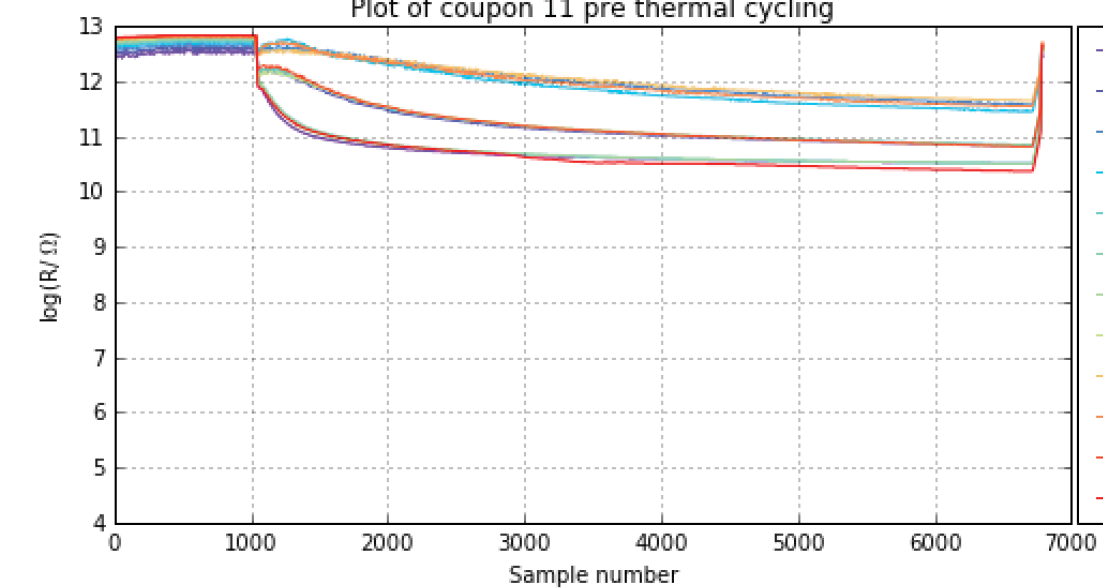
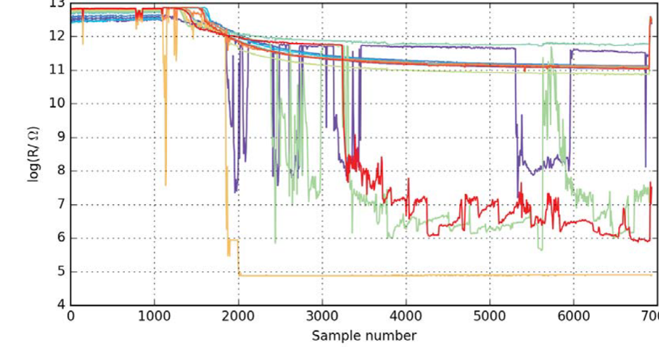 Figure 912: Insulation resistance during THB Ambient (until sample nr 1000) and THB ECM showing continuous breach of insulation on 4 patterns in the lower graph. The top graph shows stable insulation.
 Figure 913: Horizontal microsection showing fibre contamination on tracks in prepreg resin causing breach of insulation.
Conductive Anodic Filament (CAF)
General
A justification shall be provided in case any part of this test method is tailored.
The specified method can be superseded by future test campaigns to implement lessons learned or to represent applications.
Test vehicle
The lay-out of the test vehicle for CAF test shall meet all the following conditions:
- It includes the pattern configuration A as specified in Table 92 for aligned vias using ≥20x20 vias configured in X and Y-direction;
- It includes the pattern configuration B as specified in Table 93 for staggered vias using ≥10x20 vias;
- It includes the pattern configuration C as specified in Table 94 for vias in plane using ≥20x20 vias with all non-functional pads removed;
- Electrical registration coupons in X and Y-direction for verification of registration.
- 1 For requirement 9.7.3.2a.1 such comb pattern of aligned vias result in 20 vias x 19 spacing = 380 CAF opportunities within a layer.
- 2 For requirement 9.7.3.2a.2 such comb pattern of staggered vias result in 10 vias x 19 spacings x 2 manhattan paths = 380 CAF opportunities within a layer.
- 3 For requirement 9.7.3.2a.3 the C pattern of vias-in-plane is used to represent via-to-track. The non-functional pad is removed on all layers, otherwise the failure mechanism can be as for the configuration conductor-to-conductor.
- 4 For requirement 9.7.3.2a.3 C pattern is designed with bias voltage connected to the vias. Therefore the vias are positive, i.e. the anode. CAF grows from the anode, hence CAF can grow from the via, which is the purpose of this test pattern design.
- 5 For requirement 9.7.3.2a.1 test pattern A is deemed to be most susceptible to CAF.
- 6 It is good practice to implement an incremental spacing to rows of vias to avoid that the via pattern always aligns with the glass weave of the laminate.
- 7 Laser drilled microvias give less propensity for CAF compared to mechanical vias, because:
- smaller diameter and smaller contact area to glass
- less desmear
- less vibrations during hole wall formation
Based on this, testing a mechanical via is considered representative or slightly worse-case of a microvia. For microvia, the critical spacing is to a conductor, not to an adjacent microvia. This is therefore covered by test pattern C. By design, microvias can be spaced further apart than mechanical vias because of small feature size and possibility to stagger.
The build-up of the test vehicle for CAF test shall meet all the following conditions:
- Representative of the PID for material and PCB technology;
- ≥ 10 copper layers;
- 1,6 mm ± 10 % thickness over connector metallisation;
- 17 μm copper foil on inner and outer layers;
- Single sequence for drilling and plating;
- Sequential lamination.
- 1 The stack-up is laminated once, after which it passes through the lamination process for a second time to simulate sequential construction.
- 2 It is important to note in Table 92, Table 93 and Table 94 that hole diameters are specified as drill bit diameter, not finished hole diameter.
The manufacture of samples shall follow the process flow as specified in the PID.
Surface finish on connector shall not be SnPb
This is specified because SnPb can contaminate the connector pins on the test rack. Alternative finishes, such as galvanic Au and/or Ni or ENEPIG do not show this problem.
In total 10 samples shall be tested from at least two different panels.
Registration should be ≤ 80 μm.
The actual registration achieved on each coupon shall be included for the calculation of minimum insulation distances.
Table 92: CAF pattern dimensions – via-to-via straight
|
Description
|
Pattern
|
Drill diam. (µm)
|
Pad diam. (µm)
|
Via edge to via edge(µm)
|
|
X and Y-direction
|
IPC A1
|
750
|
860
|
270
|
|
IPC A2
|
650
|
810
|
370
| |
|
IPC A3
|
500
|
750
|
520
| |
|
IPC A4
|
350
|
690
|
670
| |
|
ECSS A4
|
300
|
600
|
720
|
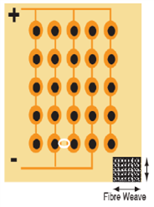
Table 93: CAF pattern dimensions – via-to-via staggered
|
Description
|
Pattern
|
Drill diam. (µm)
|
Pad diam. (µm)
|
Via edge to via edge(µm)
|
Via edge to via edge Manhattan distance (µm)
|
|
1080 pitch
|
IPC B1
|
800
|
940
|
280
|
396
|
|
IPC B2
|
700
|
890
|
380
|
537
| |
|
IPC B3
|
550
|
840
|
530
|
750
| |
|
IPC B4
|
450
|
750
|
630
|
891
| |
|
ECSS B4
|
300
|
600
|
780
|
1103
|
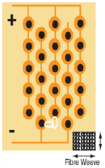
Table 94: CAF pattern dimensions – via-to-plane
|
Description
|
Pattern
|
Drill diam. (µm)
|
Pad diam. (µm)
|
Clearance diam. (µm)
|
Via edge to plane(µm)
|
|
|
IPC C1
|
350
|
none
|
640
|
145
|
|
IPC C2
|
350
|
none
|
700
|
175
| |
|
IPC C3
|
350
|
none
|
850
|
250
| |
|
IPC C4
|
350
|
none
|
960
|
305
|
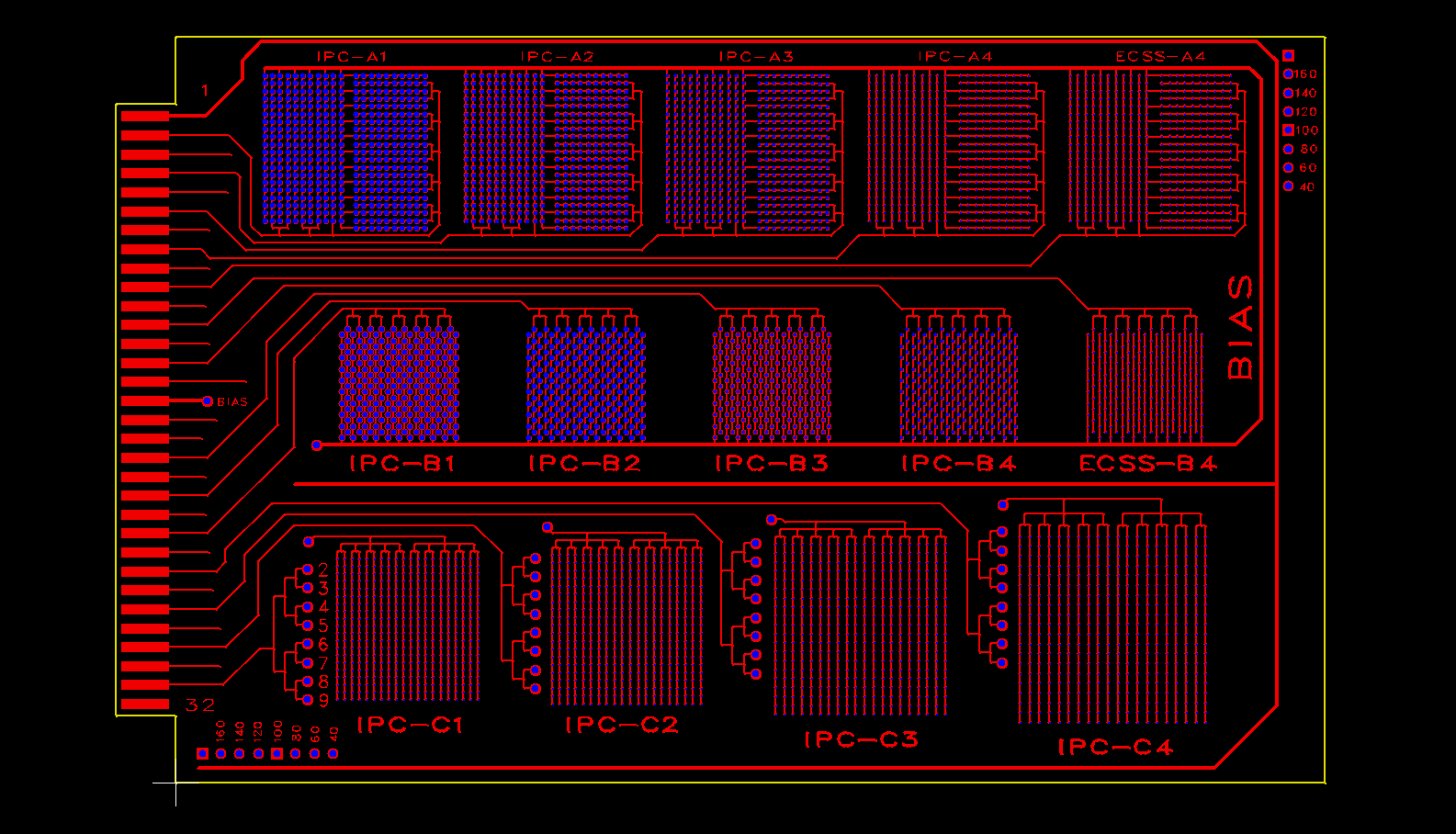 Figure 914: Lay-out of CAF pattern
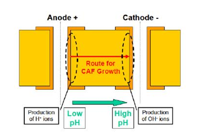 Figure 915: Schematic for CAF growth
Test method
The sample preparation method shall be as follows:
- measurement of registration on electrical test coupons;
- bake-out in conformance with clause 9.2.2;
- six times reflow simulation in conformance with clause 9.8.3;
- ultrasonic cleaning followed by bake-out in conformance with clause 9.2.2. The CAF test method shall be as follows:
- Ambient phase using the parameters: 24h, 25°C, 50% RH, 0V;
- Preconditioning phase using the parameters: 96h, 85°C, 75% RH, 0V;
- CAF phase using the parameters: 500h, 85°C, 75% RH, 50V;
- Ambient phase using the parameters: 24h, 25°C, 50% RH, 0V.
- 1 CAF is relevant for HDI which can use voltages up to 30 V in conformance with ECSS-Q-ST-70-12. The guidelines in IPC-9691B recommend a margin of x2. For practical considerations of the test equipment this is limited to 50 V.
- 2 It is good practice to control the environmental chamber such that no condensation or rain occurs. This can be achieved during the transition from the ambient phase to the pre-conditioning phase by increasing temperature at a controlled rate, implementing a dwell time, after which the humidity can be increased at a controlled rate. This can be achieved during the transition from the CAF phase to the ambient phase by decreasing the humidity at a controlled rate, implementing a dwell time, after which the temperature can be decreased at a controlled rate.
- 3 It is good practice to clean the environmental chamber and the electrical test rack and to perform a dry run at a temperature and humidity level higher than the set points during the CAF test.
During the CAF test method insulation resistance of all patterns shall be measured periodically using an electrometer capable of measuring high resistances combined with a switchbox, while maintaining the bias voltage if applicable.
The AutoSIR equipment can perform this task. It is good practice to have current limiting resistors of 1 MΩ to avoid fusing the CAF and damage to the laminate. This is foreseen in the AutoSIR.
Acquisition rate during the CAF phase shall be at least once in 15 minutes.
A faster acquisition rate is good practice to be able to detect transient changes.
During the ambient and preconditioning phases, only a few acquisitions of insulation resistance shall be done.
This is specified because bias voltage is applied during measurement, in phases that are specified to be without bias stress.
After the CAF test method, the location of breach of insulation should be determined on each pattern by electrical insulation of sections of the pattern.
Localisation in A and B pattern comprises of determining the x, y location, which can be achieved by insulation of sections of the surface pattern. Localisation in C pattern comprises of determining the layer, which can be achieved by insulation of the interconnections to the planes that are designed on the surface.
After localisation samples should be microsectioned to determine the cause of a breach of insulation resistance.
It is good practice to perform visual inspection on test rack, PCB sample connector footprint and test pattern surface area to verify that breach of insulation is not caused by surface effects, such as dendritic growth. To mitigate this risk, it is possible to apply a coating on the test pattern surface layers, such as conformal coating, solder mask or potting. On the connector footprint this risk is mitigated by only using every second connector.
Acceptance criteria
A sudden drop in resistance by an order of magnitude shall be breach of insulation.
- 1 Breach of insulation can occur intermittent or continuous. Examples of stable insulation and breach of insulation are shown in Figure 912. Breach of insulation during the first ambient phase or the pre-conditioning phase are considered early failures for which CAF cannot be the failure mechanism.
- 2 An insulation threshold below 0,1 GΩ is typically considered a breach of insulation. However, such absolute threshold depends on the sensitivity of the sample design.
Nonconformances caused by breach of insulation shall be evaluated by the qualification authority and by the procurement authority for the HDI technology under evaluation.
The test patterns have an increasingly complex design. Failure of a specific pattern can be attributed to the small spacing or the specific via configuration. It is good practice to evaluate the representativity of the failed pattern to the used HDI design. For instance, the ECSS A4 and ECSS B4 patterns are considered to be most representative to HDI designs for space and are not expected to fail. In contrast, IPC pattern A1 is designed with significantly less insulation distance than specified in ECSS-Q-ST-70-12 and can therefore be expected to show failures.
Group 6 – Assembly and life test - short
Overview
Group 6 includes a lower number of 200 thermal cycles with a higher temperature range of 200 C. It does not include electrical testing and peel strength. This thermal cycling method is quicker to perform and has heritage from ECSS-Q-ST-70-10. The group 6 is performed for delta qualification or project qualification, in case it is not necessary to cover the general assembly verification.
The test levels for thermal cycling are not only driven by space environment. Thermal cycling to the levels specified in clauses 9.6.2 and 9.8.2 provide reference to the heritage test levels that assess robustness of the PCB construction.
See clause 9.6.1 for an overview of group 4.
Test flow for group 6
The test vehicle for group 6 shall include the PCB.
A PCB with a nonconformance on external layers identified by visual inspection can be selected as test vehicle. In case the nonconformance to visual inspection criteria is not associated to thermal stress and clearly identified on the test vehicle prior to the test, it can be evaluated as a conform test result.
The test vehicle for group 6 may include additional coupons.
The following test steps shall be performed for group 6 in this order:
- bake-out in conformance with clause 9.2.2;
- reflow simulation in conformance with clause 9.8.3;
- rework simulation on at least 4 PTH of the PCB in conformance with clause 9.5.4;
- thermal cycling in conformance with clause 9.8.4;
- microsectioning in conformance with clause 9.5.2;
- evaluation of acceptance criteria in conformance with clause 10. Microsectioning and evaluation in conformance with 9.8.2c.5 and 9.8.2c.6 shall be performed on the following:
- At least 4 PTH of the PCB that have been subjected to rework simulation;
- All technology features under qualification.
In case of project qualification, the reflow simulation and rework simulation may be tailored to be representative of the assembly processes.
In case of project qualification, the reflow simulation and rework simulation shall be representative of the worst-case assembly processes.
Assembly processes include initial assembly by hand and machine soldering, as well as rework and repair.
In case of project qualification with specific environmental requirements, the thermal cycling may be tailored.
- 1 Specific environmental requirements can include operational temperature below -55 C or above +85 C, for instance for detector technology that is exposed to planetary environment.
- 2 It is not good practice to reduce the temperature range or number of cycles because thermal cycling is not only a simulation of space environment. It also simulates equipment on/off cycles and it is considered a general assessment of PCB robustness.
In case of project qualification on a PCB technology with only SMT pads and no PTH, the rework may be tailored to be performed on the SMT pads.
Reflow simulation
Reflow simulation shall be performed using a vapour phase equipment and process that are representative of assembly, except for the case in requirement 9.8.3b.
In case reflow simulation is used for a specific project qualification that uses another assembly method than vapour phase, the test method may be tailored to be representative.
The test board shall be lowered into the vapour phase at a temperature of minimum 215 C.
Specific vapour phase chemistry are commonly used with a temperature of up to 230 C.
The duration at the maximum temperature of the profile shall be between 5 s and 10 s.
The sample shall be cooled at ambient temperature for at least 10 minutes.
After cool down, the sample shall be exposed to a second reflow by repeating the steps from requirements 9.8.3c, 9.8.3d and 9.8.3e.
Thermal cycling
Thermal cycling shall be performed in a one chamber system with ambient pressure.
A temperature sensor shall be in contact with the test vehicle to monitor its temperature continuously.
The rate of temperature change shall not exceed 10 C/minute.
The dwell time at minimum and maximum temperature shall be at least 15 minutes.
The cycling programme shall start with the hot cycle first.
The temperature should be minimum -60 C and maximum +140 C.
The minimum temperature shall be between -55 C and -70 C.
This covers the assembly verification in conformance with requirement 13.3d. of ECSS-Q-ST-70-08 and 14.6 of ECSS-Q-ST-70-38.
The maximum temperature shall be between +130 C and +145 C.
The Tg of laminates is typically higher than this temperature.
The temperature range shall be at least 200 C.
The number of cycles shall be 200.
Acceptance criteria
Overview
The tables in this clause specify the technological features under evaluation. They include an identification by a reference letter, as specified in clause 4.3. The tables specify "Acceptance criteria" for the "Technological features", as well as the "Procurement inspection sample" and the "Measurement method".
The tables identify which sample is inspected for procurement. In addition other samples can be available for procurement, such as "set 2" in clause 10.2. The acceptance criteria in these tables are also applied to the other samples for procurement and qualification inspection samples.
The inspection sample includes a description of the condition, such as AR, RW, SB. In case this condition is placed in brackets, it indicates that vias with the condition in brackets are present on the coupon and are available for inspection for the technological feature, but the condition in brackets holds no relevance for the evaluation of the technological feature. This is the case for defects associated with PCB manufacture and present in AR condition when these defects are evaluated on a coupon after thermal stress that does not cause alteration of the defect.
Illustrations of measurements methods and acceptance criteria are given in photographs and drawings in the notes of the tables from clauses 10.2 to 10.4.
Inspection by microsectioning for dimensional verification
For the technological feature internal annular ring, the acceptance criteria, the inspection samples and the measurement method shall be in conformance with Table 101.
For the technological feature external annular ring, the acceptance criteria, the inspection samples and the measurement method shall be in conformance with Table 102.
For the technological feature copper foil thickness, the acceptance criteria, the inspection samples and the measurement method shall be in conformance with Table 103.
For the technological feature copper plating thickness, the acceptance criteria, the inspection samples and the measurement method shall be in conformance with Table 104.
For the technological features etchback and glass fibre protrusion, the acceptance criteria, the inspection samples and the measurement method shall be in conformance with Table 105.
For the technological feature wicking, the acceptance criteria, the inspection samples and the measurement method shall be in conformance with Table 106.
For the technological feature wrap copper, the acceptance criteria, the inspection samples and the measurement method shall be in conformance with Table 107.
For the technological feature dielectric thickness for standard technology. The acceptance criteria, the inspection samples and the measurement method shall be in conformance with Table 108.
For the technological feature dielectric thickness for microvia layers, the acceptance criteria, the inspection samples and the measurement method shall be in conformance with Table 109.
For the technological features microvia dimensions and aspect, the acceptance criteria, the inspection samples and the measurement method shall be in conformance with Table 1010.
For the technological feature microvia plating voids, the acceptance criteria, the inspection samples and the measurement method shall be in conformance with Table 1011.
For the technological features tin-led thickness and composition, the acceptance criteria, the inspection samples and the measurement method shall be in conformance with Table 1012.
For the technological features electrolytic nickel and gold dimensions, the acceptance criteria, the inspection samples and the measurement method shall be in conformance with Table 1013.
For the technological feature undercut, the acceptance criteria, the inspection samples and the measurement method shall be in conformance with Table 1014.
For the technological feature overhang, the acceptance criteria, the inspection samples and the measurement method shall be in conformance with Table 1015.
For the technological feature dimensional verification of the rigid-flex interface the acceptance criteria, the inspection samples and the measurement method shall be in conformance with Table 1016.
Table 101: Annular ring internal
|
Ref.
|
Technological feature
|
Acceptance criteria
|
Procurement inspection sample
|
Measurement method
|
|
a.
|
Inner layer
|
≥ 50 µm
|
Location: coupon A/B + Bn
|
Microsection and Microscope:
|
|
b.
|
Inner layer at end of blind via
|
≥ 50 µm
| ||
|
c.
|
Inner layer at end of buried via
|
≥ 50 µm
| ||
|
d.
|
Micro via capture pad
|
≥ 10 µm
| ||
|
e.
|
Inner layer in conformance with 10.6.1d
|
≥ 25 µm
|
Location: electrical registration in 4 corners
| |
|
Figure 101: Annular ring internal | ||||
Table 102: Annular ring external
|
Ref.
|
Technological feature
|
Acceptance criteria
|
Procurement inspection sample
|
Measurement method
|
|
a.
|
Outer layer
|
≥ 100 µm
|
Location: coupon A/B + Bn
|
Microsection and Microscope:
|
|
b.
|
Outer layer PTH solder side
|
≥ 200 µm
| ||
|
c.
|
Outer layer PTH solder side only for rigid polyimide
|
≥ 130 µm
| ||
|
d.
|
Outer layer PTH only for flex termination
|
≥ 250 µm on component hole
| ||
|
e.
|
Outer layer blind via
|
≥ 100 µm
| ||
|
f.
|
Micro via outer layer
|
≥ 10 µm
| ||
|
g.
|
Non-plated hole outer layer
|
≥ 250 µm
| ||
|
Figure 102: Annular ring external | ||||
|
Note 1: Annular ring on outer layer as specified in Ref. a from Table 102, includes vias and PTH on component side for rigid, rigid/flex and flex technology.
| ||||
Table 103: Copper foil thickness
|
Ref.
|
Technological feature
|
Acceptance criteria
|
Procurement inspection sample
|
Measurement method
| |
|
|
Nominal copper foil thickness
|
Minimum measured copper foil thickness after processing
|
Location: coupon A/B + Bn
|
Microsection and Microscope:
| |
|
a.
|
70 µm
|
≥ 56 µm
| |||
|
b.
|
35 µm
|
≥ 25 µm
| |||
|
c.
|
17 µm
|
≥ 11 µm
| |||
|
d.
|
12 µm for HDI
|
≥ 9 µm
| |||
|
e.
|
9 µm for HDI
|
≥ 6 µm
| |||
|
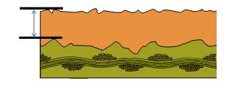
Figure 103: Copper foil thickness |
The microetching and passivation on the top surface is not subtracted from the thickness measurement.
| ||||
|
Note 1: The equivalent IPC test method is described in IPC-A-600 test method 3.2.4 and IPC-6012D chapter 3.6.2.15
| |||||
Table 104: Copper plating thickness
|
Ref.
|
Technological feature
|
Acceptance criteria
|
Procurement inspection sample
|
Measurement method
| |
|
a.
|
Electroplated copper in PTH and through going vias
|
Rigid
|
≥ 25 µm average on resin
|
Location: coupon A/B + Bn
|
Microsection and Microscope:
|
|
b.
|
Flexible
|
≥ 25 µm average on resin
| |||
|
c.
|
Rigid-flex
|
≥ 30 µm average on resin
| |||
|
d.
|
Electroplated copper in blind and buried via
|
≥ 25 µm average on resin
| |||
|
e.
|
Electroplated copper over base copper for layers with plated holes
|
≥ 25 µm
| |||
|
f.
|
Electroplated copper over base copper for internal layers with only microvias
|
≥ 5 µm
| |||
|
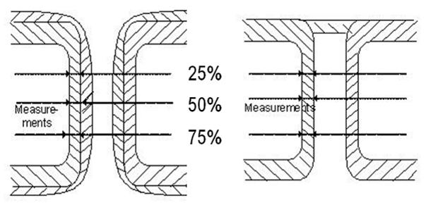
Figure 104: Three measurements of copper plating thickness at locations that are at 25 %, 50 % and 75 % of the height of the hole
| |||||
|
Note 1: There is no additional requirement for total copper thickness on surface. As an example for Ref. e. min copper foil after processing is 11 μm, plus 25 μm plated copper, results in min 36 μm total copper thickness for standard technology.
| |||||
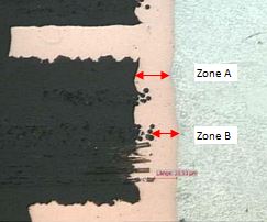
Table 105: Etchback and glass fibre protrusion
|
Ref.
|
Technological feature
|
Acceptance criteria
|
Procurement inspection sample
|
Measurement method
|
|
a.
|
Etchback
|
Between negative -13 µm and positive +20 µm
|
Location: coupon A/B + Bn
|
Microsection and Microscope:
|
|
b.
|
Glass fibre protrusion, in case of negative etchback
|
Glass fibres should protrude into hole wall relative to the resin
| ||
|
c.
|
Glass fibre protrusion, in case of positive etchback
|
Glass fibres should protrude into hole wall relative to the inner layer
| ||
|
d.
|
Glass fibre protrusion
|
Glass fibre protrusion should be limited such that the requirement for minimum Cu plating thickness is achieved.
| ||
|
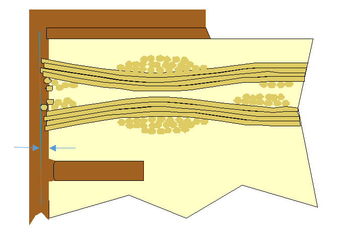
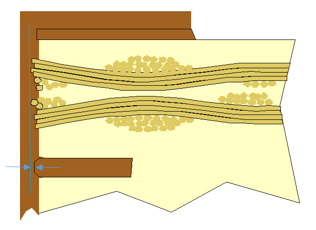
Figure 106: Glass fibre protrusion in case of negative etchback (left) and positive etchback (right)
| ||||
|
Note 1: Glass fibre protrusion is a qualitative assessment of the general aspect of the hole. A single occurrence outside requirement is not a nonconformance if the general aspect meets the requirement.
| ||||
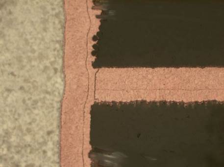
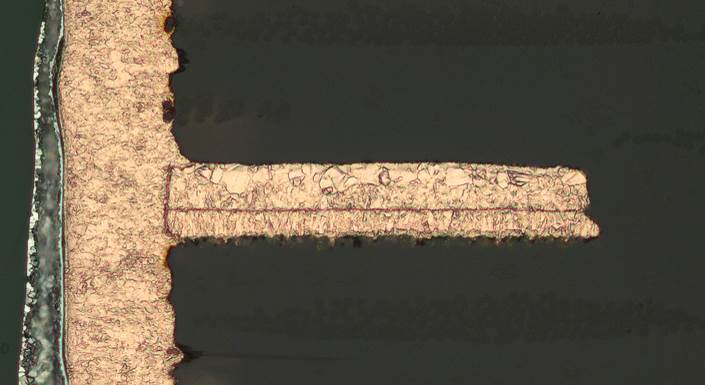
Table 106: Wicking
|
Ref.
|
Technological feature
|
Acceptance criteria
|
Sample
|
Measurement method
|
|
a.
|
Wicking on standard technology
|
≤ 50 µm
|
Location: coupon A/B + Bn
|
Microsection and Microscope:
|
|
b.
|
Wicking on reduced annular ring of ≥ 25 μm
|
≤ Min annular ring
| ||
|
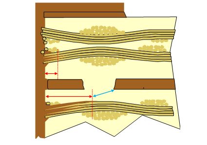
Figure 108: Wicking is measured from resin of hole wall (red arrows). In case it exceeds the annular ring, the insulation distance to adjacent circuitry (blue arrow) can be reduced. |
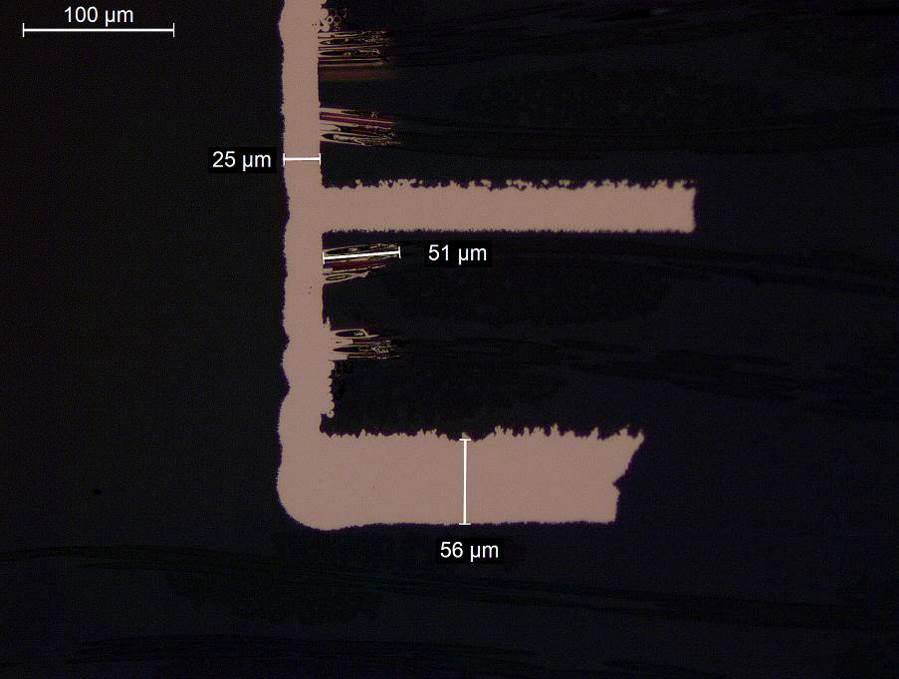
Figure 109: Example of wicking | |||
Table 107: Wrap copper
|
Ref.
|
Technological feature
|
Acceptance criteria
|
Procurement inspection sample
|
Measurement method
| |
|
a.
|
Copper wrap thickness
|
≥ 5µm wrap thickness
|
Location: coupon Bn
|
Microsection and Microscope:
| |
|
b.
|
Copper wrap length
|
≥ 25µm wrap length
| |||
|
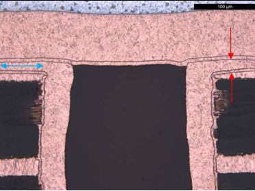
Figure 1010: Wrap target condition |
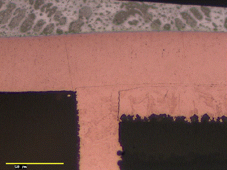
Figure 1011: Wrap thickness below requirement, not acceptable | ||||
|
Note: Planarization or selective plating can be in the PCB manufacturer’s PID, if the copper wrap criteria from this table are met. Insufficient wrap copper indicates too much planarization. This can cause separation in plating layers due to lack of mechanical strength.
| |||||
Table 108: Dielectric thickness – standard technology
|
Ref.
|
technological feature
|
Acceptance criteria
|
Procurement inspection sample
|
Measurement method
| |
|
a.
|
Insulation between layers
|
≥ 70 µm for rigid
|
Location: coupon A/B + Bn
|
Microsection and Microscope:
| |
|
b.
|
Number of prepreg between layers
|
≥ 2
| |||
|
c.
|
Number of glass layers in laminate
|
should be ≥ 2, i.a.w. ECSS-Q-ST-70-12 requirement 7.1.3b.
| |||
|
d.
|
Glass fibre compression
|
not acceptable in case track is compressed into glass bundle and resin starvation occurs
| |||
|
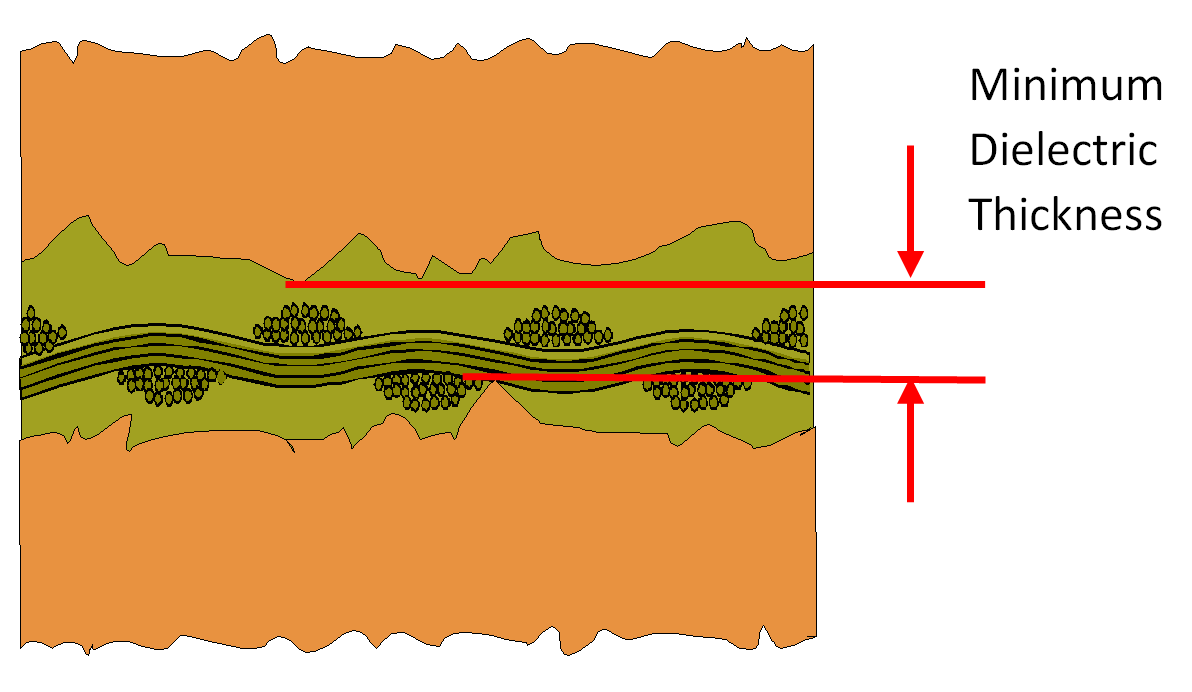
Figure 1012:Projected-peak-to-peak insulation |
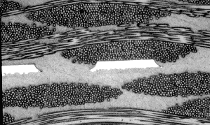
Figure 1013: Example of glass compression | ||||
Table 109: Dielectric thickness – microvia layers
|
Ref.
|
Technological feature
|
Acceptance criteria
|
Procurement inspection sample
|
Measurement method
| |
|
a.
|
Insulation between layers
|
≥ 60 µm
|
Location: coupon Bn
|
Microsection and Microscope:
| |
|
b.
|
Number of prepreg
|
2
| |||
|
c.
|
Penetration of capture pad
|
Complete penetration through pad not acceptable
| |||
|
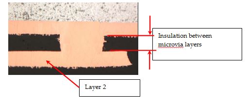
Figure 1014: Microvia insulation |
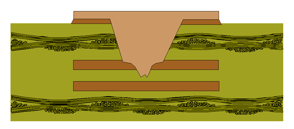
Figure 1015: Penetration of capture pad for µvia, not acceptable | ||||
|
Note: Dielectric thickness of approximately 60 µm can create a risk for glass compression. A typical maximum of 120 µm can be used to accommodate 20 % tolerance on the maximum as-designed thickness of 100 µm, in conformance with req 11.4i. from ECSS-Q-ST-70-12. The maximum thickness is in addition limited by the requirement for aspect ratio ≤ 1 of microvias, in conformance with Ref. c. from Table 1010. In case of high dielectric thickness there can be a risk not to meet the contact diameter of 100 µm in conformance with Ref. d. from Table 1010.
| |||||
Table 1010: Dimension and aspect of microvias
|
Ref.
|
Technological feature
|
Acceptance criteria
|
Procurement inspection sample
|
Measurement method
| ||
|
a.
|
Dimple
|
≤ 30 µm
|
Location: coupon Bn
|
Microsection and Microscope:
| ||
|
b.
|
Bump
|
≤ 15 µm
| ||||
|
c.
|
Aspect ratio
|
≤ 1
| ||||
|
d.
|
Contact diameter to capture pad
|
≥ 100 µm continuous contact
| ||||
|
e.
|
Interconnect defect from microvia to capture pad
|
not acceptable
|
Microsection and Microscope:
| |||
|
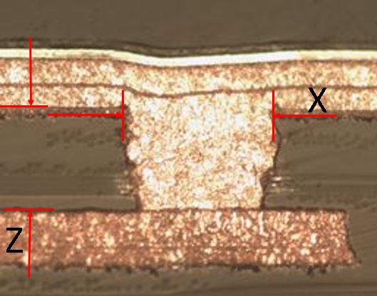
X=laser drilled diameter in layer 1 base copper, Z=distance from top of layer 1 base copper to top of capture pad copper
|
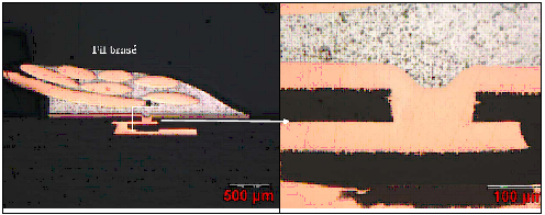
Figure 1017: Dimple in microvia |
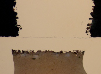
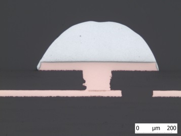
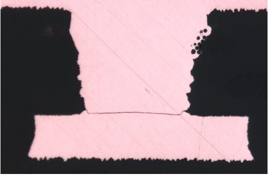
Figure 1018: ICD on capture pad (pictures are unetched) | ||||
|
Note 1: Microvias can show resin or glass at the bottom edge. This is not considered a defect in case 100 μm continuous contact is achieved. Presence of dielectric material is not considered ICD.
| ||||||
Table 1011: Microvia plating voids
|
Ref.
|
Technological feature
|
Acceptance criteria
|
Procurement inspection sample
|
Measurement method
| |
|
a.
|
Void inside copper filled microvia
|
Target condition: no voids.
|
Location: coupon Bn
|
Microsection and Microscope:
| |
|
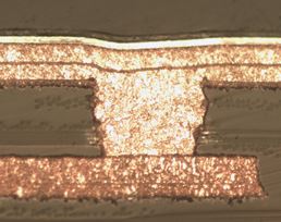
Figure 1019: Microvia plating, target condition |
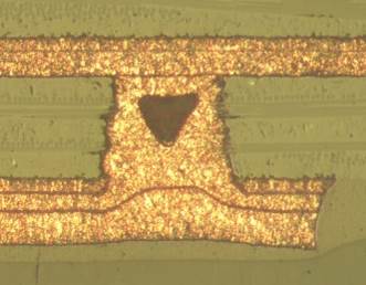
Figure 1020: Example of void in microvia plating | ||||
|
Note 1: Allowance for voiding is specified in this table for a relatively low sample size as done for procurement. In qualification a larger sample size is taken to verify that the target condition is achieved.
| |||||
Table 1012: Tin-lead thickness and composition
|
Ref.
|
Technological feature
|
Acceptance criteria
|
Procurement inspection sample
|
Measurement method
| |
|
a.
|
SnPb composition
|
Tin content 63±8% by weight
|
Location: coupon A/B
|
Ref. a: XRF, SEM-EDX, atomic absorption spectrometry on bare PCB
| |
|
b.
|
SnPb thickness on SMT pads
|
≥ 5 µm on thickest area
| |||
|
c.
|
SnPb thickness on PTH hole wall
|
≥ 8 µm on thickest area
| |||
|
d.
|
SnPb thickness on PTH corners
|
≥ 1 µm excluding the IMC
| |||
|
e.
|
SnPb thickness on PTH pads
|
≥ 5 µm
| |||
|
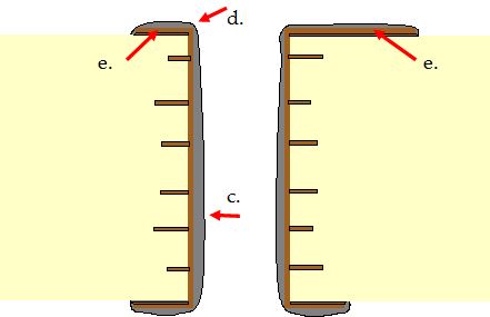
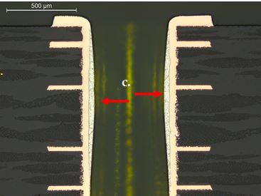
Figure 1021: Tin-lead thickness in PTH schematic (left) and a typical microsection (right) | |||||
|
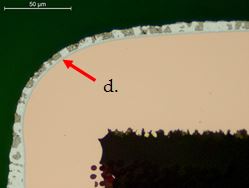
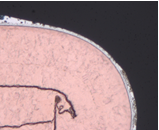
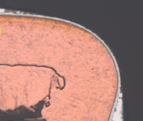
Figure 1022: Tin-lead thickness on PTH corner – target thickness (left), coverage of less than 1 µm (middle), absence of SnPb on IMC (right) | |||||
|
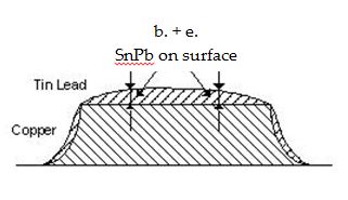
Figure 1023: Tin-lead thickness on pad |
Measurement is done in centre of pad, at the thickest area.
| ||||
|
Note 1: Ref. d allows for less than 1 μm SnPb thickness as long as the IMC is covered by SnPb and acceptable solderability test is obtained.
| |||||
Table 1013: Dimensional requirements for electrolytic and chemical Ni, Pd, Au
|
Ref.
|
Technological feature
|
Acceptance criteria
|
Procurement inspection sample
|
Measurement method
|
|
a.
|
Electrolytic nickel
|
≥ 2 µm on all locations, and
|
Location: PCB or coupon A/B or dedicated coupon
|
XRF on PCB, or
|
|
b.
|
Electrolytic gold on nickel
|
≥ 1 µm
| ||
|
c.
|
Electrolytic gold on copper
|
≥ 3 µm
| ||
|
d.
|
Length of tin-lead overlap on Au
|
≥ 150 µm
| ||
|
e.
|
ENIG
|
Ni 3-6 µm
|
1,5x1,5 mm2 as per IPC-4552A
|
XRF as per IPC-4552A
|
|
f.
|
ENEPIG
|
Ni 4-6 µm
|
1,5x1,5 mm2 as per IPC-4556
|
XRF as per IPC-4556
|
|
g.
|
ENIPIG
|
Ni 3-7 µm
|
1,5x1,5 mm2 as per IPC-4556
|
XRF as per IPC-4556
|
|
Note 1: It is not good practice to use gold as surface finish for soldering as per ECSS-Q-ST-70-08 requirements 6.6.2a and 6.8.2a.
| ||||
Table 1014: Undercut and spurious copper
|
Ref.
|
Technological feature
|
Acceptance criteria
|
Procurement inspection sample
|
Measurement method
|
|
a.
|
Undercut on internal layers
|
u ≤ h
|
Location: coupon A/B + Bn
|
Microsection and Microscope:
|
|
b.
|
Undercut on external layers
|
u ≤ h
| ||
|
c.
|
Undercut on external layers
|
u ≤ h
| ||
|
d.
|
Spurious copper
|
Incidental occurrence of copper from the rough side of the foil is acceptable if < 10 µm
| ||
|
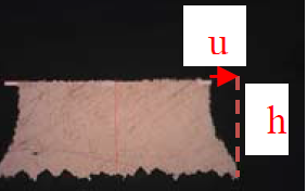
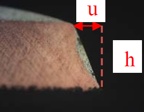
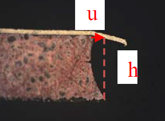
Ref. a Ref. b Ref. c
| ||||
|
Note Spurious copper can be caused by inefficient etching. This is not the same as copper residue as described in Table 1039. This is not the same as dotted interface line as described in Ref. e of Table 1033.
| ||||
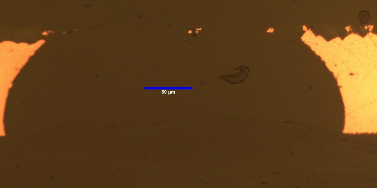
Table 1015: Overhang
|
Ref.
|
Technological feature
|
Acceptance criteria
|
Procurement inspection sample
|
Measurement method
|
|
a.
|
Overhang on reflowed Sn/Pb finish
|
No overhang
|
Location: coupon A/B + Bn
|
Microsection and Microscope:
|
|
b.
|
Overhang on electrolytic Ni/Au or Au finish
|
D ≤ 2x total thickness of copper (h) in case of conformal coating as per 10.6.3j
| ||
|
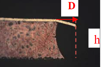
Figure 1026: Overhang of electrolytic Au | ||||
|
Note: For Tin-lead finish during the reflow operation the overhang of Tin-lead is flowing on the side of the tracks or pads: if the reflow operation has been well conducted there is no overhang left.
| ||||
Table 1016: Rigid-flex interface -dimensional verification
|
Ref.
|
Technological feature
|
Acceptance criteria
|
Procurement inspection sample
|
Measurement method
|
|
a.
|
Coverlay and bond-ply insertion into rigid section i.a.w. ECSS-Q-ST-70-12 req. 9.4c.
|
≥ 1 mm
|
Location: rigid-flex coupon
|
Microsection and Microscope
|
|
b.
|
Distance between hole wall and rigid edge of interface, i.a.w. ECSS-Q-ST-70-12 req. 9.5a.
|
≥ 2mm
| ||
|
c.
|
Overlap between coverlay and pad, i.a.w. ECSS-Q-ST-70-12 req. 9.4e.
|
Not acceptable
| ||
|
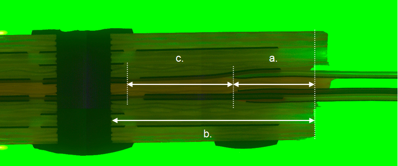
Figure 1027: Example of dimensional verification of rigid-flex interface | ||||
|
Note 1: In case coverlay insertion into rigid section is 2 mm and distance between hole wall and rigid edge is 2mm then the coverlay overlaps the pad and requirement is not achieved. Requirement 9.4d from ECSS-Q-ST-70-12 specifies that in a multilayer rigid-flex PCB where flex laminates are bonded together with bond-ply, the ends of the coverlay and bond-ply are off- set in the rigid section by 1 mm to prevent a line of weakness.
| ||||
Inspection by microsectioning for qualitative aspects
For the technological feature via filling the acceptance criteria, the inspection samples and the measurement method shall be in conformance with Table 1017.
For the technological feature cap lift, the acceptance criteria, the inspection samples and the measurement method shall be in conformance with Table 1018.
For the technological feature blind via planarity, the acceptance criteria, the inspection samples and the measurement method shall be in conformance with Table 1019.
For the technological features burrs and nodules, the acceptance criteria, the inspection samples and the measurement method shall be in conformance with Table 1020.
For the technological features voids and inclusions in copper plating the acceptance criteria, the inspection samples and the measurement method shall be in conformance with Table 1021.
For the technological features wedge voids the acceptance criteria, the inspection samples and the measurement method shall be in conformance with Table 1022.
For the technological feature resin voids, the acceptance criteria, the inspection samples and the measurement method shall be in conformance with Table 1023.
For the technological features delamination, blistering, crazing and measling, the acceptance criteria, the inspection samples and the measurement method shall be in conformance with Table 1024.
For the technological feature pad lift, the acceptance criteria, the inspection samples and the measurement method shall be in conformance with Table 1025.
For the technological feature dielectric cracks, the acceptance criteria, the inspection samples and the measurement method shall be in conformance with Table 1026.
For the technological features cracks and separation in copper, the acceptance criteria, the inspection samples and the measurement method shall be in conformance with Table 1027.
For the technological feature ICD, the acceptance criteria, the inspection samples and the measurement method shall be in conformance with Table 1028.
For the technological feature smear, the acceptance criteria, the inspection samples and the measurement method shall be in conformance with Table 1029.
For the technological features hole wall pull away and resin recession, the acceptance criteria, the inspection samples and the measurement method shall be in conformance with Table 1030.
For the technological feature nail heading, the acceptance criteria, the inspection samples and the measurement method shall be in conformance with Table 1031.
For the technological feature copper-invar-copper, the acceptance criteria, the inspection samples and the measurement method shall be in conformance with Table 1032.
For the technological feature inhomogeneity in dielectric, the acceptance criteria, the inspection samples and the measurement method shall be in conformance with Table 1033.
For the technological features contamination and foreign inclusions, the acceptance criteria, the inspection samples and the measurement method shall be in conformance with Table 1034.
For the technological feature rigid-flex interface delamination between coverlay and prepreg, the acceptance criteria, the inspection samples and the measurement method shall be in conformance with Table 1035.
For the technological feature rigid-flex interface adhesive voids in coverlay and bond-ply, the acceptance criteria, the inspection samples and the measurement method shall be in conformance with Table 1036.
For the technological feature rigid-flex interface misalignment of prepreg, the acceptance criteria, the inspection samples and the measurement method shall be in conformance with Table 1037.
Table 1017: Blind, buried and plugged via filling
|
Ref.
|
Technological feature
|
Acceptance criteria
|
Procurement inspection sample
|
Measurement method
|
|
a.
|
Voids or cracks in the resin of blind , buried or plugged vias inside zone A
|
Target condition: no voids, no cracks
|
Location: coupon A/B + Bn
|
Microsection and Microscope:
|
|
b.
|
Voids or cracks in the resin of blind, buried or plugged vias outside zone A
|
Voids at open ends, as shown in Figure 1029, are not acceptable
| ||
|
Voids in contact with cap plating, as shown in Figure 1029, are not acceptable
| ||||
|
c.
|
Separation between hole wall and resin inside blind and buried via
|
Not acceptable AR or after SB.
| ||
|
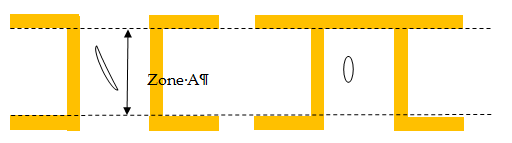
Figure 1028: Examples of acceptable voids |
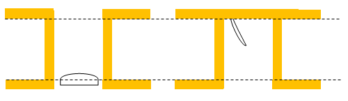
Figure 1029: Examples of unacceptable voids | |||
|
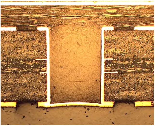
Figure 1030: Examples of separation between hole wall and resin inside blind via | ||||
|
Note 1: The via filling can be performed by resin flowing from the prepreg or by pre-filling using ink or plugging paste.
| ||||
Table 1018: Cap lift on blind via and plugged via
|
Ref.
|
Technological feature
|
Acceptance criteria
|
Procurement inspection sample
|
Measurement method
| |
|
a.
|
Cap lift (bulging)
|
Not acceptable in case via-in-pad are used for soldering as per 6.2.3e
|
Location: coupon A/B + Bn
|
Microsection and Microscope:
| |
|
b.
|
Thin line separation
|
Acceptable as received and after solder bath float up to 3 µm separation
| |||
|
c.
|
Copper surface plating thickness on resin
|
≥ 25 µm in conformance with Ref. e. from Table 104
| |||
|
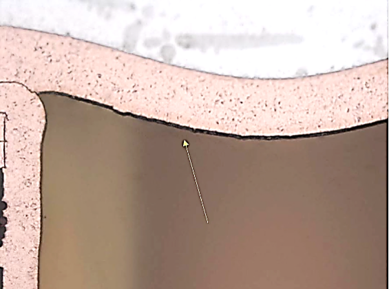
Figure 1031: Example of acceptable thin line separation |
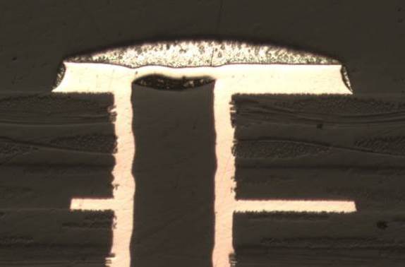
Figure 1032: Example of non-acceptable bulging | ||||
Table 1019: Blind and plugged via planarity
|
Ref.
|
Technological feature
|
Acceptance criteria
|
Procurement inspection sample
|
Measurement method
|
|
a.
|
Dimple of via
|
Depth of dimple ≤ 50 µm
|
Location: coupon A/B + Bn
|
Microsection and Microscope:
|
|
b.
|
Bump on via
|
≤ 15 µm
| ||
|
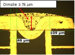

Figure 1033: Example of dimple on blind via |

Figure 1034: Example of bump on blind via | |||
|
Note 1: Superpositioning of blind vias in PCB is represented in coupons in conformance with requirement 15.2d.5(c) from ECSS-Q-ST-70-12.
| ||||
Table 1020: Burrs and nodules
|
Ref.
|
Technological feature
|
Acceptance criteria
|
Procurement inspection sample
|
Measurement method
|
|
a.
|
Burrs and nodules
|
Not acceptable if diameter of plated hole is reduced to below the requirement
|
Location: coupon A/B
|
Microsection and Microscope:
|
|
Not acceptable if detached by probing with a gauge
| ||||
|
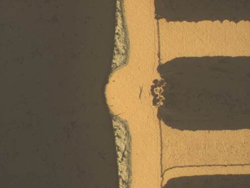
Figure 1035: Example of plating nodule |
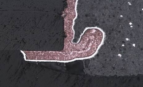
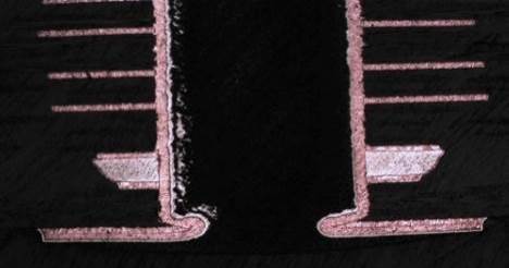
Figure 1036: Example of burrs reducing hole diameter | |||
|
Note 1: It is good practice to avoid the presence of burrs and nodules because they can have a negative impact on reliability of the PTH as evaluated in IST.
| ||||
Table 1021: Voids and inclusions in copper plating
|
Ref.
|
Technological feature
|
Acceptance criteria
|
Procurement inspection sample
|
Measurement method
| |
|
a.
|
Voids and inclusions in copper plating
|
Target condition: no voids, no inclusions
|
Location: coupon A/B + Bn
|
Microsection and Microscope:
| |
|
b.
|
Skip plating
|
Target condition: no skip plating
| |||
|
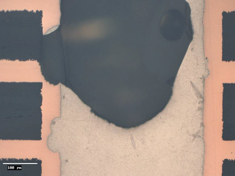
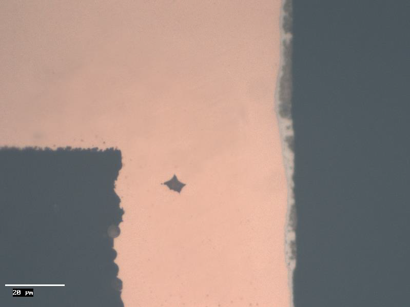 Figure 1037: Example of voids – top image shows etch-out and bottom image shows an encapsulated void or inclusion |
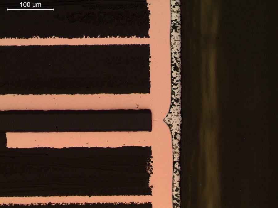
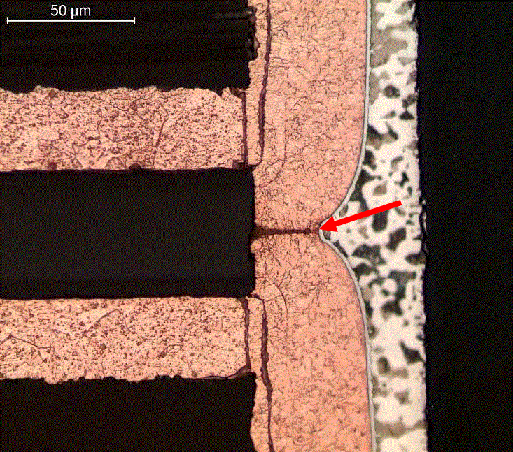
Figure 1038: Skip plating on flex laminate as-polished (top) and after micro-etch (bottom)
| ||||
|
Note: Skip plating can be caused by electroless copper that does not cover local areas of the hole wall, such as glass fibres or flex laminate. Subsequent galvanic copper layers can cover up the skip plating, in which case the requirement for minimum copper thickness on local thin areas can be achieved. This can be observed as a plating fold in an etched microsection. On an unetched microsection the copper can seem continuous.
| |||||
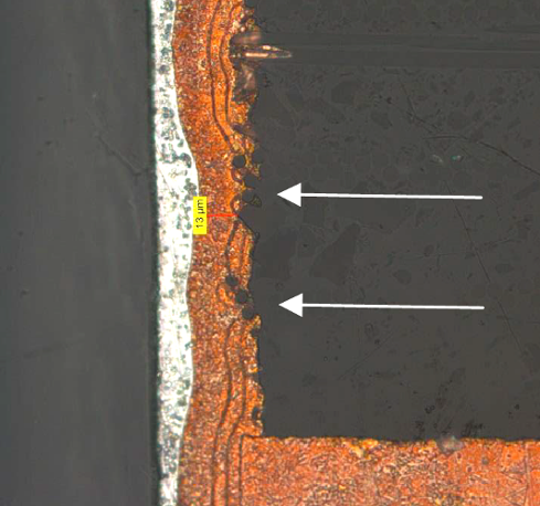
Table 1022: Wedge voids
|
Ref.
|
Technological feature
|
Acceptance criteria
|
Procurement inspection sample
|
Measurement method
| ||
|
a.
|
Open wedge void
|
Not acceptable
|
Location: coupon A/B + Bn
|
Microsection and Microscope:
| ||
|
b.
|
Enclosed wedge void
|
Acceptable on PCB manufacturer copper treatment side of foil in case:
| ||||
|
c.
|
Copper filled wedge
|
Acceptable on PCB manufacturer copper treatment side of foil in case:
| ||||
|
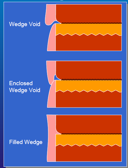
Figure 1040: Open wedge void (top), enclosed wedge void (middle), copper filled wedge (bottom) |
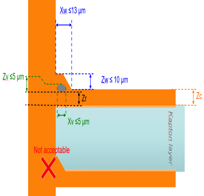
Xw: wedge depth
|
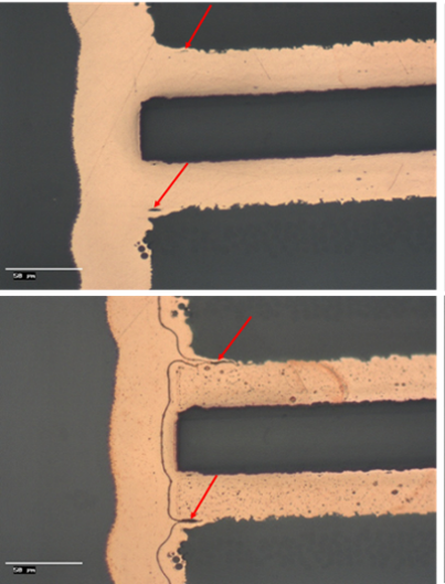
Figure 1042: Example of wedge voids | ||||
|
Note 1: The height of the copper wedge voids is determined from the copper foil to the point on the hole wall that is aligned with the drilling through the resin.
| ||||||
Table 1023: Resin void
|
Ref.
|
Technological feature
|
Acceptance criteria
|
Procurement inspection sample
|
Measurement method
|
|
a.
|
Resin voids
|
Target condition: no voids
|
Location: coupon A/B + Bn
|
Microsection and Microscope:
|
|
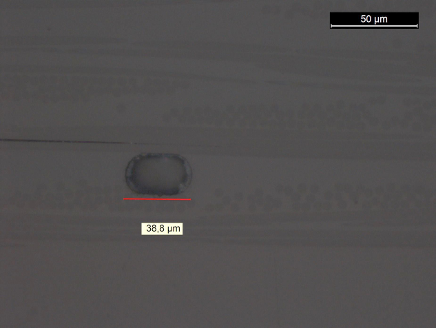
Figure 1043: Example of resin void | ||||
|
Note: Resin voids can occur in prepreg as well as laminate
| ||||
Table 1024: Delamination, blistering, crazing, measling
|
Ref.
|
Technological feature
|
Acceptance criteria
|
Procurement inspection sample
|
Measurement method
|
|
a.
|
Delamination, blistering, crazing, measling
|
Not acceptable
|
Location: coupon A/B + Bn
|
Microsection and Microscope:
|
|
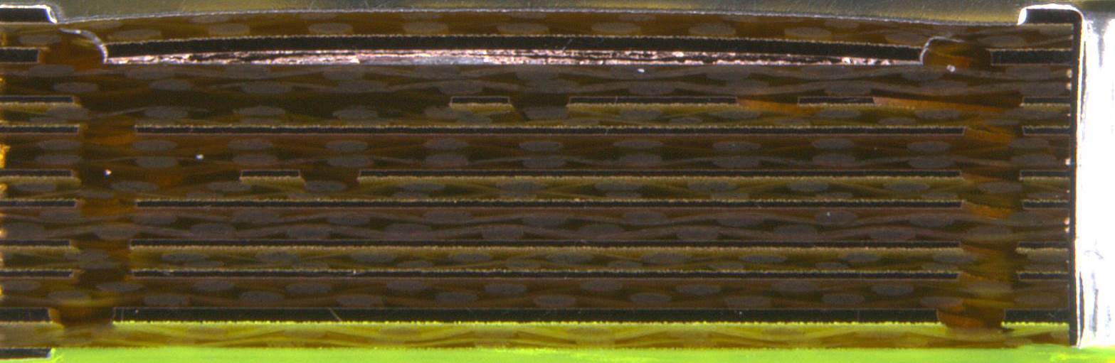
Figure 1044: Example of delamination | ||||
|
Note : These defects are also evaluated during visual inspection as per Table 1041.
| ||||
Table 1025: Pad Lift
|
Ref.
|
Technological feature
|
Acceptance criteria
|
Procurement inspection sample
|
Measurement method
|
|
a.
|
Pad lift and cracks associated with pad lift
|
Acceptable if all the following conditions are met:
|
Location: coupon A/B + Bn
|
Microsection and Microscope
|
|

Figure 1045: Pad lift schematic
| ||||
|
Note 1: The background for pad lift to occur on epoxy technology is because the Tg of the material is below the solidification temperature of solder. Therefore the thermal expansion (above Tg) is high, while the solder has already solidified (during cooling). These conditions are not valid on polyimide laminate, for instance, which has a higher Tg. In case pad lift occurs on polyimide it is considered to be an indicator of an anomaly of the process or the material.
| ||||
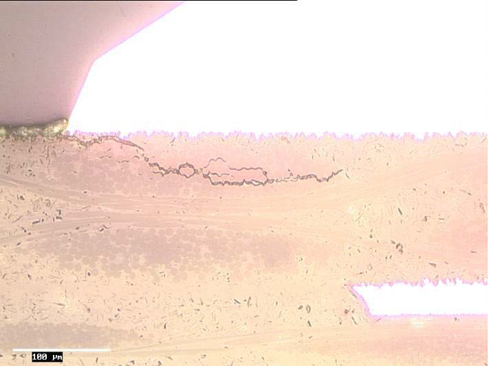
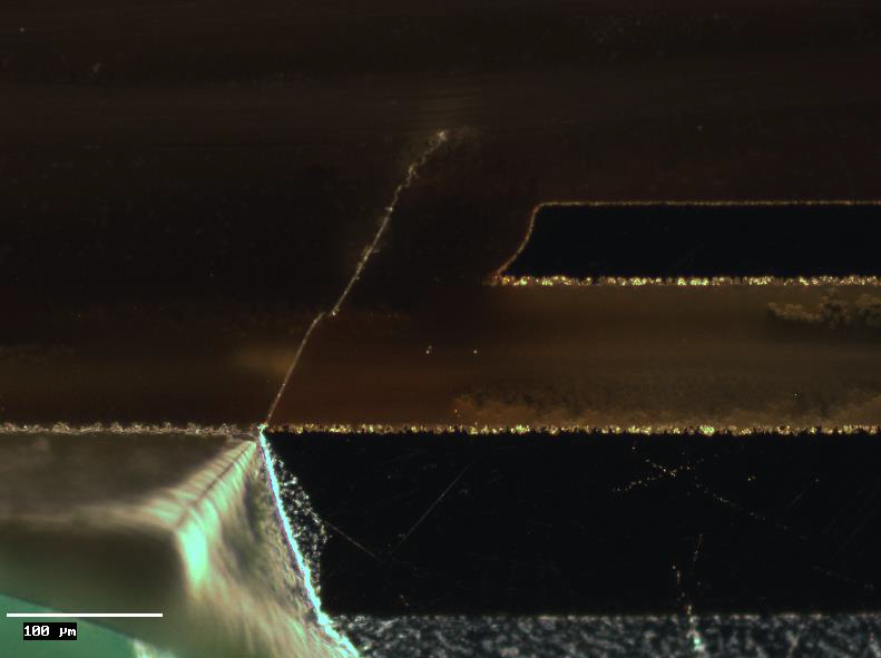
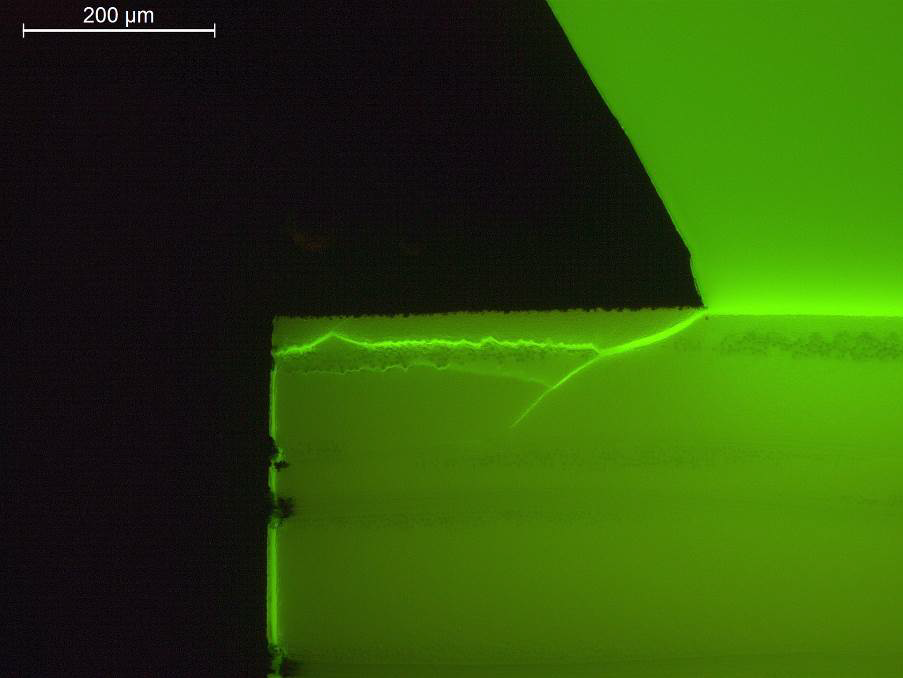
Table 1026: Dielectric cracks
|
Ref.
|
Technological feature
|
Acceptance criteria
|
Procurement inspection sample
|
Measurement method
|
|
a.
|
Drilling crack
|
Standard PCB technology: acceptable if ≤ 80 µm
|
Location: coupon A/B + Bn
|
Microsection and Microscope
|
|
b.
|
Crack associated with the end of a conductor pattern
|
≤ 80 µm and referee test 4 microsections in the spare PCB after SB does not show cracks more than 80 µm, as per 10.6.3c.
| ||
|
c.
|
Random cracks in the dielectric
|
≤ 80 µm and referee test 4 microsections in the spare PCB after SB does not show cracks, , as per 10.6.3c.
| ||
|
d.
|
Crack (for Ref. a, b, c)
|
not crossing glass reinforcement in Z-direction
| ||
|
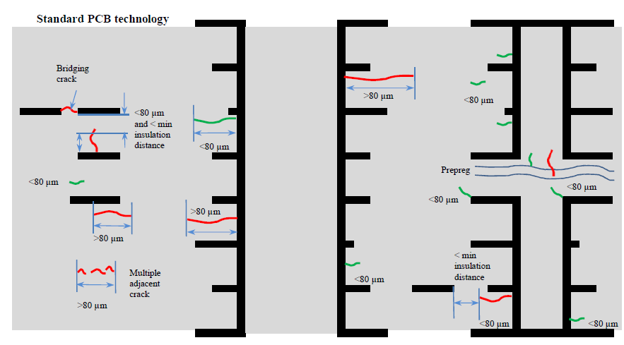
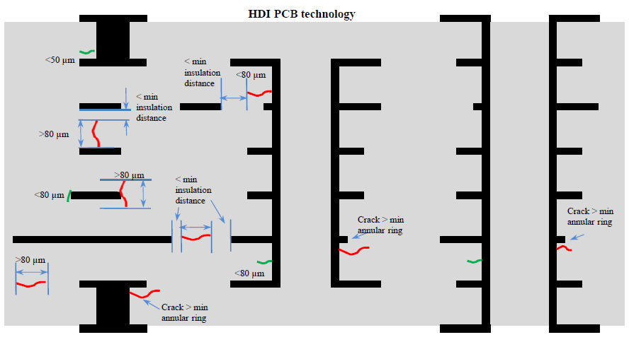
Figure 1047: Acceptable (green) and non-acceptable (red) dielectric cracks
| ||||
|
Note 1: The PCB definition dossier is in conformance with the DRD of ECSS-Q-ST-70-12 Annex A. The insulation distance specified in the PCB definition dossier is in conformance with ECSS-Q-ST-70-12 Table 13-7.
| ||||
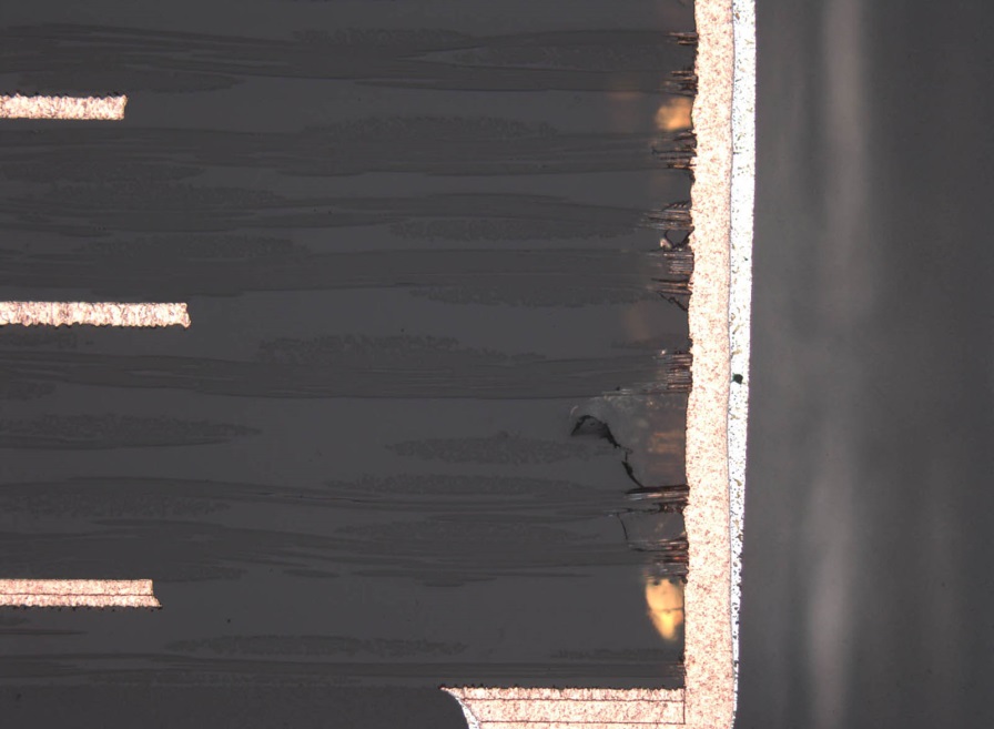
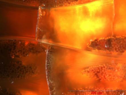
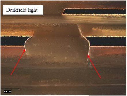
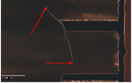
Table 1027: Cracks and separation in copper
|
Ref.
|
Technological feature
|
Acceptance criteria
|
Procurement inspection sample
|
Measurement method
|
|
a.
|
Cracks in internal and external copper foil
|
Not acceptable
|
Location: coupon A/B + Bn
|
Microsection and Microscope
|
|
b.
|
Cracks in copper plating including barrel cracks and corner cracks
| |||
|
c.
|
Separation between external copper foil and copper plating
|
Not acceptable AR, RW, SB
| ||
|
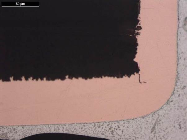
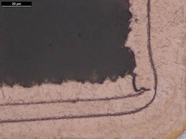
Figure 1049: Example of C foil separation as-polished and after micro-etch
| ||||
|
Note : Interface lines between copper plating layers can occur. ECSS-Q-ST-70-60 does not specify an accept or reject criterion for such feature. It can be justified by group 6 for qualification.
| ||||
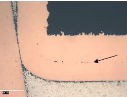
Table 1028: Interconnect defect, ICD
|
Ref.
|
Technological feature
|
Acceptance criteria
|
Procurement inspection sample
|
Measurement method
|
|
a.
|
Interconnect defect
|
Not acceptable
|
Location: coupon A/B and Bn
|
Microsection and Microscope:
|
|
b.
|
ICD in microvia
|
See Table 1010 Ref. e.
| ||
|
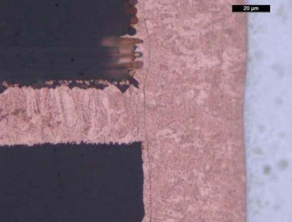
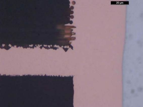 Figure 1051: Interconnect after stress, target condition, after microetch (top) and as-polished (bottom) |

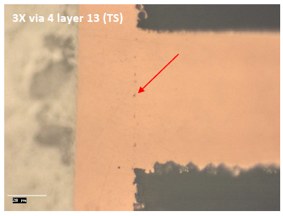 Figure 1052: Examples of ICD | |||
|
Note1: It is important for this type of defect that microsections are evaluated in as-polished condition. Microetching can be done to determine the exact interface once a defect has been observed. However, an etched microsection is not suitable for initial evaluation for ICD since it always shows an interface line between foil and plating.
| ||||
Table 1029: Smear
|
Ref.
|
Technological feature
|
Acceptance criteria
|
Procurement inspection sample
|
Measurement method
|
|
a.
|
Smear
|
Polyimide and Epoxy: no smear accepted
|
Location: coupon A/B + Bn
|
Microsection and Microscope:
|
|
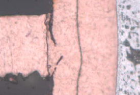
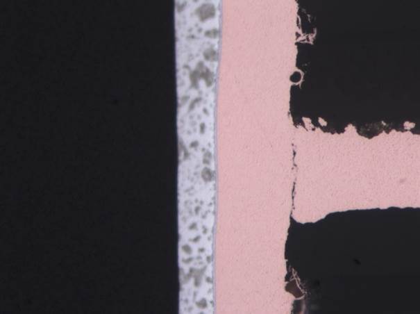
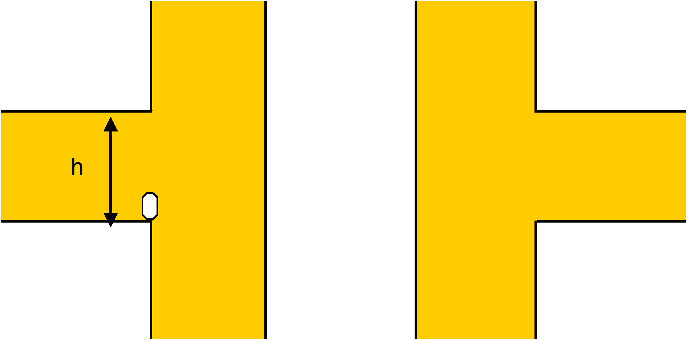
Figure 1053: Example of smear | ||||
|
Note: In case 10-25 % smear is observed, an additional horizontal microsection is taken to verify the extent of smear around the circumference.
| ||||
Table 1030: Hole wall pull away and resin recession
|
Ref.
|
Technological feature
|
Acceptance criteria
|
Procurement inspection sample
|
Measurement method
| |
|
a.
|
Hole wall pull away
|
≤ 20 % of the sum of dielectric on standard layers is acceptable
|
Location: coupon A/B + Bn
|
Microsection and Microscope
| |
|
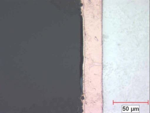
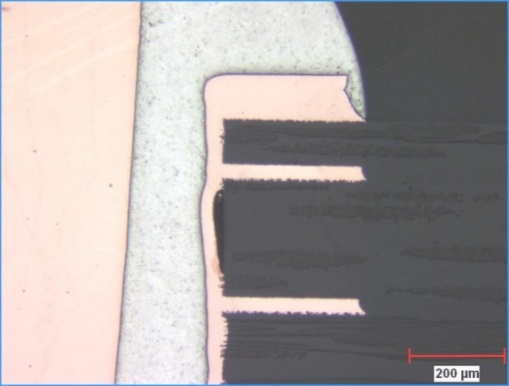
Figure 1054: Example of hole wall pull away - showing separation of copper in a straight line (left) or slightly bulging outward (right) |
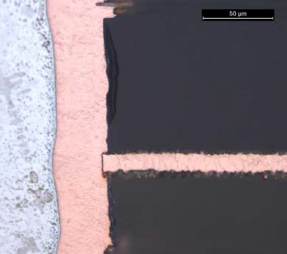
Figure 1055: Example of resin recession - showing concave retraction of resin | ||||
|
Note 1 Group 6 on hole wall pull away or resin recession is performed to show absence of cracks in copper and separation between hole wall and resin within the requirement.
| |||||
Table 1031: Nail heading
|
Ref.
|
Technological feature
|
Acceptance criteria
|
Procurement inspection sample
|
Measurement method
| ||
|
a.
|
Nail heading
|
≤ 50 % of inner layer copper thickness
|
Location: coupon A/B + Bn
|
Microsection and Microscope:
| ||
|
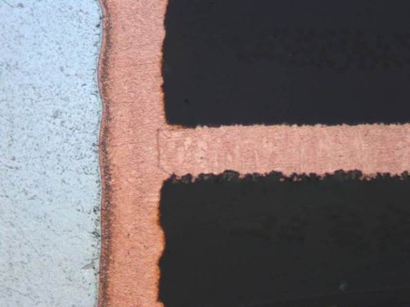
Figure 1056: Target condition |
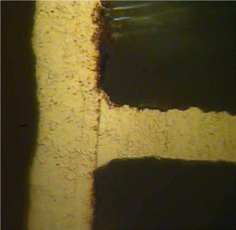
Figure 1057: Acceptable nail heading |
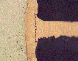
Figure 1058:Unacceptable nail heading, exceeding 50 % of innerlayer copper thickness | ||||
Table 1032: Cu-Invar-Cu
|
Ref.
|
Technological feature
|
Acceptance criteria
|
Procurement inspection sample
|
Measurement method
|
|
a.
|
Nailheading in CIC layers
|
≤ 50 % of copper thickness on CIC layer
|
Location: coupon A/B + Bn
|
Microsection and Microscope:
|
|
b.
|
Separation or contamination between copper on CIC layer and plated barrel
|
No separation or contamination allowed
| ||
|
c.
|
Separation or contamination between Invar layer and plated barrel
|
≤ 20 % separation/contamination
| ||
|
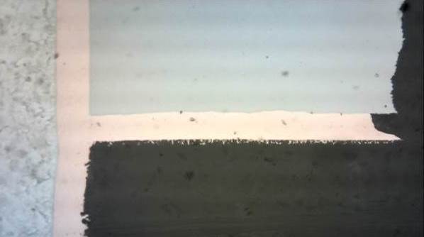
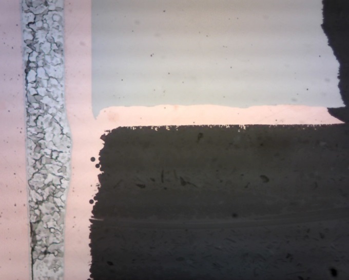
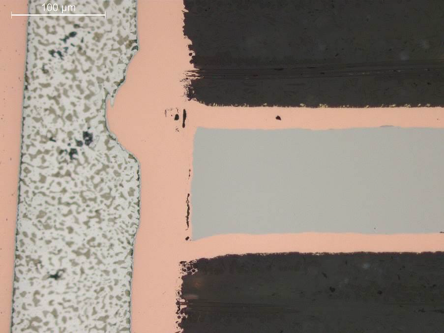
Figure 1059: Examples of CIC connection, target condition (left), nailheading (middle), separation to CIC (right) | ||||
|
Note: Contamination can be Invar smear, seen as a grey substance between copper and plated barrel
| ||||
Table 1033: Inhomogeneity in dielectric
|
Ref.
|
Technological feature
|
Acceptance criteria
|
Procurement inspection sample
|
Measurement method
|
|
a.
|
Agglomeration of bromine flame retardant
|
Unacceptable
|
Location: coupon A/B + Bn
|
Microsection and Microscope:
|
|
b.
|
Agglomeration of filler
|
Unacceptable in case size is >80 µm on interface between prepreg and laminate
| ||
|
c.
|
Swirl or milky appearance in no-flow prepreg
|
Acceptable in case its evaluation is recorded in the PID.
| ||
|
d.
|
Demarcation line in no-flow prepreg
|
Acceptable in case its evaluation is recorded in the PID.
| ||
|
e.
|
Dotted interface line
|
Acceptable in case all the following conditions are met:
|
Microsection and Microscope:
| |
|

Figure 1060: Examples of swirl (1st and 2nd image) and demarcation line (3rd). In the 2nd picture the difference between no-flow prepreg (top) and laminate (bottom) is noticeable
| ||||
|
Note 1: Cracks are evaluated in conformance with Table 1026.
| ||||
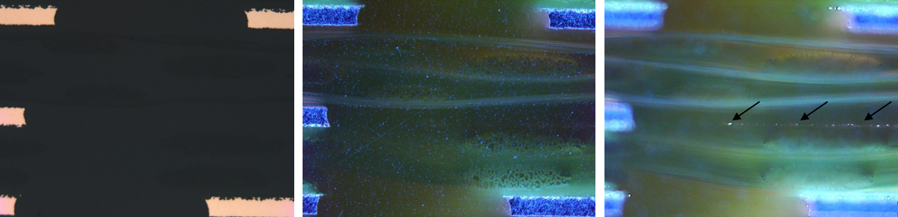
Table 1034: Contamination or foreign inclusion
|
Ref.
|
Technological feature
|
Acceptance criteria
|
Procurement inspection sample
|
Measurement method
|
|
a.
|
Non-metallic contamination in microsection
|
Target condition: no contamination
|
Location: coupon A/B + Bn
|
Microsection and Microscope:
|
|
b.
|
Metallic contamination
|
Not acceptable
| ||
|
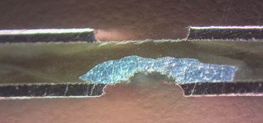
Figure 1062: Example of metallic contamination in laminate | ||||
|
Note: This is specified to handle all types of contamination. Because of the inspection by cross-sectioning it is most effective at detecting larger inclusions. Small fibre contamination cannot be efficiently evaluated in a cross-section. Instead it can be better evaluated by visual inspection in conformance with Table 1042 on external layers. Internal layer cleanliness is also specified in clause 6.5 and 6.7.
| ||||
Table 1035: Rigid-flex interface - delamination between coverlay and prepreg
|
Ref.
|
Technological feature
|
Acceptance criteria
|
Procurement inspection sample
|
Measurement method
|
|
a.
|
Delamination between coverlay and prepreg
|
Not accepted
|
Location: rigid-flex coupon
|
Microsection and Microscope:
|
|
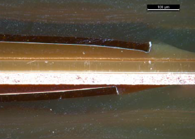
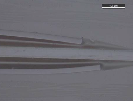
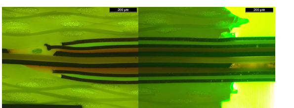
Figure 1063: Acceptable adhesion between coverlay and prepreg
| ||||
|
Note 1: Preparation of the microsection can create separation between materials due to mechanical stress.
| ||||
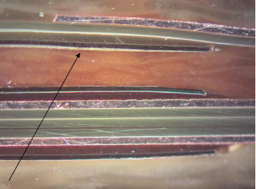
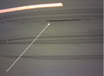
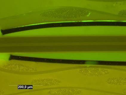
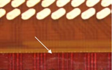
Table 1036: Rigid-flex interface - adhesive voids in coverlay and bond-ply
|
Ref.
|
Technological feature
|
Acceptance criteria
|
Procurement inspection sample
|
Measurement method
|
|
a.
|
Adhesive void in Rigid-flex interface
|
Target condition: no voids
|
Location: rigid-flex coupon
|
Microsection and Microscope:
|
|
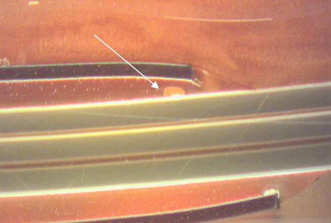
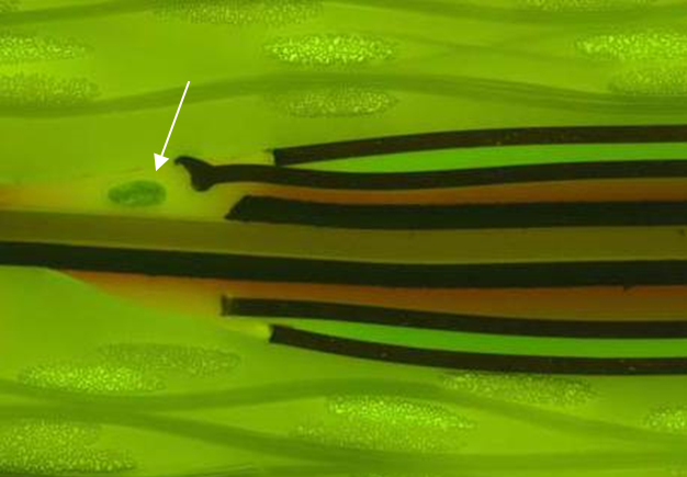
Figure 1065 Example of voids in acrylic adhesive in rigid-to-flex interface | ||||
|
Note: Bond-ply consist of kapton with adhesive on both sides as indicated in the note of requirement 9.3e of ECSS-Q-ST-70-12. Only adhesive between copper layers does not provide sufficient insulation.
| ||||
Table 1037: Rigid-flex interface - misalignment of prepreg
|
Ref.
|
Technological feature
|
Acceptance criteria
|
Procurement inspection sample
|
Measurement method
|
|
a.
|
Resin squeeze out
|
≤ 1,5 mm
|
Location: rigid-flex coupon
|
Microsection under magnification
|
|
b.
|
Adhesive filet recession
|
≤ 0,5 mm into rigid section
| ||
|
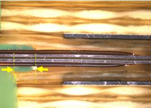
Figure 1066: Example of adhesive filet recession into rigid section as observed in microsection | ||||
|
Note: These features are also evaluated in visual inspection in conformance with Table 1048.
| ||||
Visual inspection
For the technological feature conductor width, the acceptance criteria, the inspection samples and the measurement method shall be in conformance with Table 1038.
For the technological feature conductor spacing, the acceptance criteria, the inspection samples and the measurement method shall be in conformance with Table 1039.
For the technological feature surface metallisation the acceptance criteria, the inspection samples and the measurement method shall be in conformance with Table 1040.
For the technological features measling, crazing, blistering and delamination the acceptance criteria, the inspection samples and the measurement method shall be in conformance with Table 1041.
For the technological features contamination and inhomogeneity, the acceptance criteria, the inspection samples and the measurement method shall be in conformance with Table 1042.
For the technological feature scratches, the acceptance criteria, the inspection samples and the measurement method shall be in conformance with Table 1043.
For the technological features weave exposure, the acceptance criteria, the inspection samples and the measurement method shall be in conformance with Table 1044.
For the technological feature haloing the acceptance criteria, the inspection samples and the measurement method shall be in conformance with Table 1045.
For the technological feature tin-lead surface quality the acceptance criteria, the inspection samples and the measurement method shall be in conformance with Table 1046.
For the technological feature marking the acceptance criteria, the inspection samples and the measurement method shall be in conformance with Table 1047.
For the technological features rigid-flex interface misalignment of prepreg, the acceptance criteria, the inspection samples and the measurement method shall be in conformance with Table 1048.
For the technological feature rigid-flex interface fibre protrusion the acceptance criteria, the inspection samples and the measurement method shall be in conformance with Table 1049.
For the technological feature rigid-flex interface haloing the acceptance criteria, the inspection samples and the measurement method shall be in conformance with Table 1050.
For the technological features rigid-flex interface aspect of flex laminate and coverlay the acceptance criteria, the inspection samples and the measurement method shall be in conformance with Table 1051.
Table 1038: Conductor width
|
Ref.
|
Technological feature
|
Acceptance criteria
|
Procurement inspection sample
|
Measurement method
| |
|
a.
|
Peak, nick, pinhole
|
Acceptable if all the following conditions are met:
|
Location: PCB
|
Visual inspection magnification ≥ 10x
| |
|
b.
|
Conductor width
|
Tolerance of conductor width is ≤ 20 % in conformance with Table 7-3 from ECSS-Q-ST-70-12
| |||
|
c.
|
Peak, nick, pinhole on SMD pad
|
Not acceptable in pristine area consisting of the middle 80 % of the pad
| |||
|
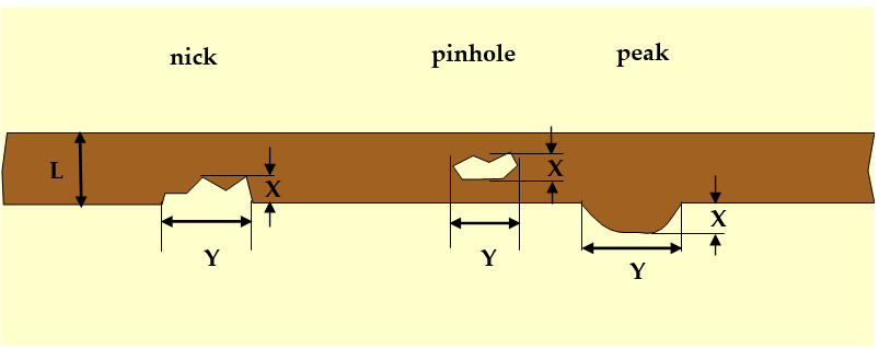
Figure 1067: Conductor width |
X: width of defect
| ||||
|
Note 1: Intermittent and irregular metallisation defects on conductors include edge roughness caused by peak (synonyms: spike, protrusions , unintentional pattern) or nick (synonyms: indentations, mouse bites, dents) and pinholes (synonyms: voids, pits). Conductors include pads.
| |||||
Table 1039: Conductor spacing
|
Ref.
|
Technological feature
|
Acceptance criteria
|
Procurement inspection sample
|
Measurement method
| |
|
a.
|
Peaks
|
Acceptable if all the following conditions are met:
|
Location: PCB
|
Visual inspection magnification ≥ 10x
| |
|
b.
|
Conducting island
|
Acceptable if all the following conditions are met:
| |||
|
c.
|
Conductor spacing
|
Tolerance of conductor spacing is ≤ 20 % in conformance with Table 7-3 from ECSS-Q-ST-70-12
| |||
|
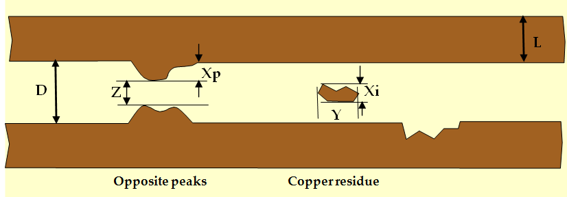
Figure 1068: Conductor spacing |
Xp: width of peak
| ||||
|
Note: Intermittent and irregular metallisation defects caused by peaks (synonyms: spikes, protrusions , unintentional pattern) or copper residue (synonyms: unintentional pattern, conducting island). Conductors include pads. Copper residue can be caused by a problem in the imaging processes. This is not the same as spurious copper as described in Table 1014.
| |||||
Table 1040: Surface metallization
|
Ref.
|
Technological feature
|
Acceptance criteria
|
Procurement inspection sample
|
Measurement method
| |
|
a.
|
Lifting or delamination of conductive pattern from substrate
|
Not accepted
|
Location: PCB
|
Visual inspection magnification ≥ 10x
| |
|
b.
|
Copper or nickel visible on top surface plated areas
|
Not accepted
| |||
|
c
|
Exposed copper on side of conductor
|
Acceptable
| |||
|
d.
|
Corrosion of exposed copper
|
Not accepted
| |||
|
Figure 1069: Example of lifted land |
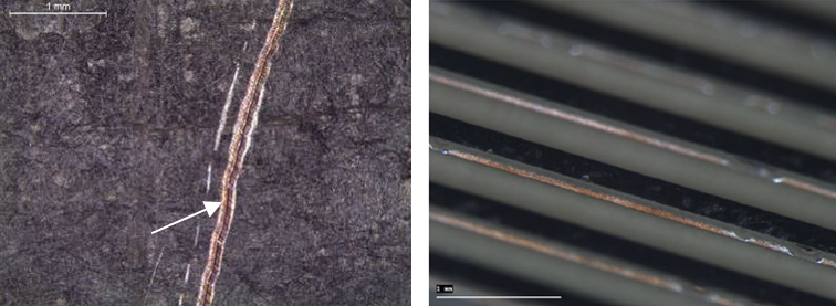
Figure 1070: Example of visible copper on top surface (left) and on side of track (right) | ||||
Table 1041: Measling, crazing, blistering, delamination
|
Ref.
|
Technological feature
|
Acceptance criteria
|
Procurement inspection sample
|
Measurement method
| |
|
a.
|
Measling, crazing, blistering, delamination
|
Not accepted
|
Location: PCB
|
Visual inspection magnification ≥ 10x
| |
|
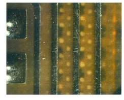
Figure 1071: Example of measling |
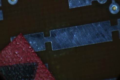
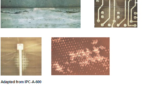
Figure 1072: Examples of crazing | ||||
|
Note: An isolated white spot is not typical for measling or crazing. Instead, this can be a dry spot, which is not associated with thermal stress, and can be evaluated as inhomogeneity. Measling can be caused by soldering and inadequate bake-out.
| |||||
Table 1042: Contamination, inhomogeneity
|
Ref.
|
Technological feature
|
Acceptance criteria
|
Procurement inspection sample
|
Measurement method
|
|
a.
|
Non-metallic contamination or inhomogeneity
|
Accepted with traceability in CoC in case the remaining insulation distance is in conformance with the PCB definition dossier.
|
Location: PCB
|
Visual inspection magnification ≥ 10x
|
|
b.
|
Metallic contamination
|
Not accepted
| ||
|
c.
|
Discoloured copper oxide on underlying layer
|
Accepted
| ||
|
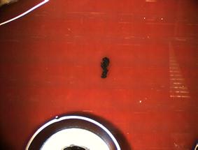
Figure 1073: Examples of contamination and inhomogeneity | ||||
|
Note 1: The term inhomogeneity is used to describe a different aspect (such as colour) of dielectric material that can be intrinsic to the material, instead of caused by a foreign substance. Discoloured copper oxide is not an inhomogeneity in the dielectric.
| ||||
Table 1043: Scratches
|
Ref.
|
Technological feature
|
Acceptance criteria
|
Procurement inspection sample
|
Measurement method
|
|
a.
|
Scratches on conductors
|
Target condition: no scratches
|
Location: PCB
|
Visual inspection magnification ≥ 10x
|
|
b.
|
Scratches on dielectric
|
Target condition: no scratches
| ||
|
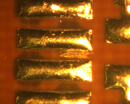
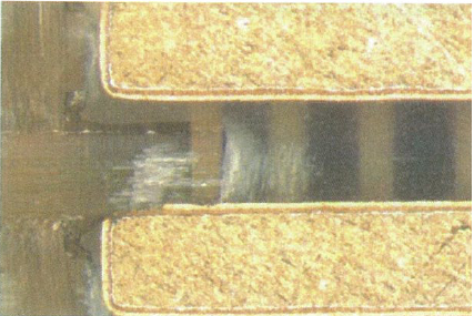
Figure 1074: Example of scratches on conductors and dielectric | ||||
|
Note: The term scratch refers also to dents and indentations. A cut of conductors is evaluated as a scratch exposing copper. Intentional scratches caused by repair are covered by the clause 6.10. Exposed glass or re-enforcement in laminate not accepted, due to risk for moisture absorption.
| ||||
Table 1044: Weave exposure
|
Ref.
|
Technological feature
|
Acceptance criteria
|
Procurement inspection sample
|
Measurement method
|
|
a.
|
Weave exposure
|
Not acceptable in external layers
|
Location: PCB
|
Visual inspection magnification ≥ 10x
|
|
b.
|
Weave texture
|
Acceptable
| ||
|
no example pictures available
| ||||
|
Note 1: It can be difficult to distinguish weave texture from weave exposure. See IPC-A-600J clause 2.2.2.
| ||||
Table 1045: Haloing at PCB edge and non-plated holes
|
Ref.
|
Technological feature
|
Acceptance criteria
|
Procurement inspection sample
|
Measurement method
|
|
a.
|
Haloing adjacent to tracks, pads and planes
|
≤ 1,5mm into rigid section, and
|
Location: PCB
|
Visual inspection magnification ≥ 10x
|
|
b.
|
Haloing adjacent to footprint for stiffener
|
≤ 90% of the insulation between edge of rigid section to pattern on external layer, and
| ||
|
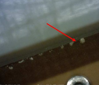
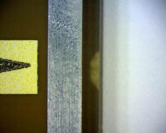
Figure 1075: Haloing at edge |
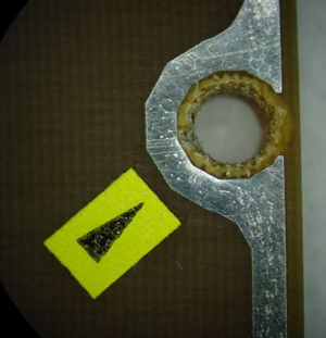
Figure 1076: Haloing from non-plated hole to footprint for stiffener | |||
|
Note 1: Depanelisation by cutting of support tabs can cause haloing.
| ||||
Table 1046: Tin-lead surface quality
|
Ref.
|
Technological feature
|
Acceptance criteria
|
Procurement inspection sample
|
Measurement method
| |
|
a.
|
Dewetting and non-wetting
|
Not accepted on solder pads
|
Location: PCB
|
Visual inspection magnification ≥ 10x
| |
|
b.
|
Granular aspects in tin-lead
|
Accepted in case sample with granular aspect pass solderability test
| |||
|
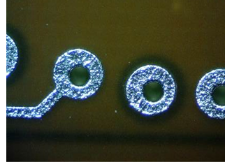
Figure 1077: Granular aspect |
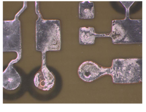
Figure 1078: Dewetting | ||||
|
Note: Granular tin-lead is caused by the temperature profile during reflow.
| |||||
Table 1047: Marking, identification
|
Ref.
|
Technological feature
|
Acceptance criteria
|
Procurement inspection sample
|
Measurement method
|
|
a.
|
Marking quality
|
Clear and legible marking
|
Location: PCB
|
Visual inspection magnification ≥ 10x
|
|
Figure 1079: Example of unclear marking | ||||
Table 1048: Rigid-flex interface - misalignment of prepreg
|
Ref.
|
Technological feature
|
Acceptance criteria
|
Procurement inspection sample
|
Measurement method
| |
|
a.
|
Resin squeeze out
|
≤ 1,5 mm
|
Location: PCB
|
Visual inspection magnification ≥ 10x
| |
|
b.
|
adhesive filet recession
|
≤ 0,5 mm into rigid section
| |||
|
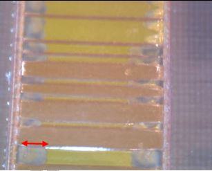
Figure 1080: Example of resin squeeze out |
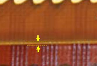
Figure 1081: Example of adhesive filet recession into rigid section as observed in visual inspection | ||||
|
Note: Resin can be squeezed out of the prepreg during lamination and flow onto the coverlay of the flex section.
| |||||
Table 1049: Rigid-flex interface - fibre protrusion
|
Ref.
|
Technological feature
|
Acceptance criteria
|
Procurement inspection sample
|
Measurement method
|
|
a.
|
Fibre protrusion
|
Target condition: smooth edge
|
Location: PCB, rigid-flex coupon
|
Visual inspection magnification ≥ 10x
|
|
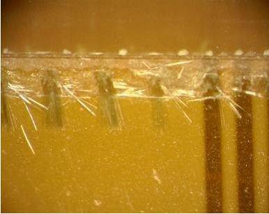
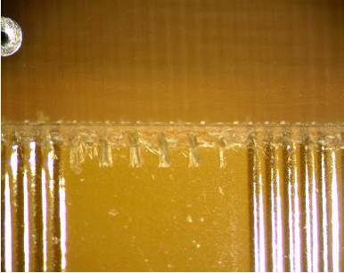
Figure 1082: Examples of fibre protrusion | ||||
|
Note: Fibre protrusion can be caused by milling when resin is removed but fibres are not cut cleanly.
| ||||
Table 1050: Rigid-flex interface - haloing
|
Ref.
|
Technological feature
|
Acceptance criteria
|
Procurement inspection sample
|
Measurement method
|
|
a.
|
Haloing
|
≤ 1,0 mm into rigid section, and
|
Location: PCB, rigid-flex coupon
|
Visual inspection magnification ≥ 10x
|
|
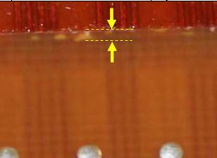
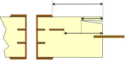
Figure 1083: Example of acceptable incidental haloing ≤ 1 mm into rigid section | ||||
|
Note 1: Haloing can be seen on all rigid edges. At the rigid-flex interface haloing can be caused by the unsupported milling process. It is good practice to allow for haloing on rigid-to-flex interface and other PCB edges when designing insulation distance from the pattern on external layer and the underlying layer to the edge.
| ||||
Table 1051: Rigid-flex - aspect of flex laminate and coverlay
|
Ref.
|
Technological feature
|
Acceptance criteria
|
Procurement inspection sample
|
Measurement method
|
|
a.
|
Scratches, folding marks, blistering, nicks, contamination, voids, white spots
|
Target condition of coverlay is without defect. An incidental defect is acceptable in accordance with the criteria specified hereunder.
|
Location: PCB, rigid-flex coupon
|
Visual inspection magnification ≥ 10x
|
|
b.
|
Scratches, cuts
|
Accepted if superficial scratch
| ||
|
c.
|
Folding marks
|
Accepted if remaining insulation distance is in conformance with PCB definition dossier.
| ||
|
d.
|
Blistering (bubbles)
|
Accepted if remaining insulation distance is in conformance with PCB definition dossier.
| ||
|
e
|
Delamination
|
not acceptable
| ||
|
f.
|
Nicks and burrs on flex edge
|
acceptable if ≤ 50 % of the insulation between edge of flex section to pattern
| ||
|
g.
|
Tear on flex edge
|
not acceptable
| ||
|
h.
|
Voids or pinhole in the kapton of the coverlay
|
Voids or pinholes are acceptable in case:
| ||
|
i.
|
Contamination below coverlay
|
Accepted if remaining insulation distance is in conformance with PCB definition dossier.
| ||
|
j.
|
Voids in adhesive from coverlay
|
Voids of ≤ 80 µm are acceptable in case the insulation distance is in conformance with the PCB definition dossier
| ||
|
k.
|
White spots below coverlay
|
Accepted if remaining insulation distance is in conformance with PCB definition dossier.
| ||
|
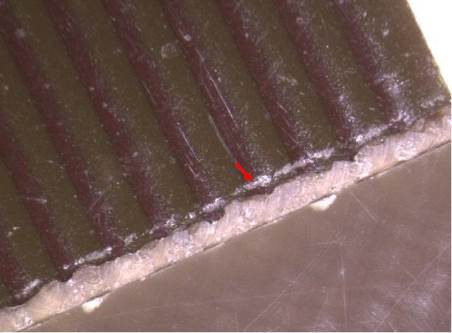
Figure 1084: Example of an acceptable superficial scratch
| ||||
|
Note 1: The PCB definition dossier is in conformance with the DRD of ECSS-Q-ST-70-12 Annex A. The insulation distance specified in the PCB definition dossier is in conformance with ECSS-Q-ST-70-12 Table 13-7.
| ||||
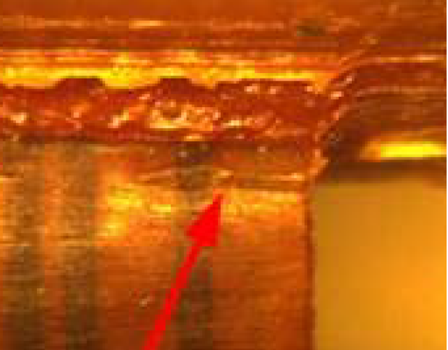
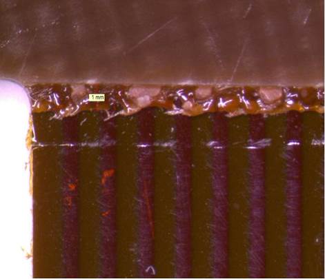
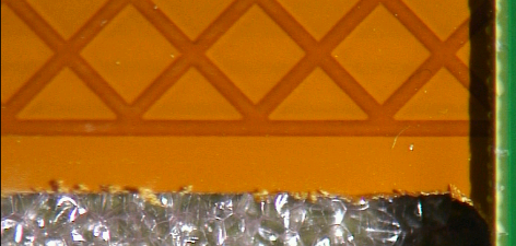
Visual inspection of sculptured flex PCB
For the technological feature misregistration of holes for sculptured flex PCB the acceptance criteria, the inspection samples and the measurement method shall be in conformance with Table 1052.
For the technological feature aspect of coverlay for sculptured flex PCB, the acceptance criteria, the inspection samples and the measurement method shall be in conformance with Table 1053.
For the technological feature tin-lead infiltration for sculptured flex PCB, the acceptance criteria, the inspection samples and the measurement method shall be in conformance with Table 1054.
For the technological feature bare copper for sculptured flex PCB, the acceptance criteria, the inspection samples and the measurement method shall be in conformance with Table 1055.
For the technological feature misregistration between pads for sculptured flex PCB, the acceptance criteria, the inspection samples and the measurement method shall be in conformance with Table 1056.
For the technological feature annular ring for sculptured flex PCB, the acceptance criteria, the inspection samples and the measurement method shall be in conformance with Table 1057.
For the technological features conductor width and spacing for sculptured flex PCB, the acceptance criteria, the inspection samples and the measurement method shall be in conformance with Table 1058.
For the technological feature adhesive in plated holes for sculptured flex PCB, the acceptance criteria, the inspection samples and the measurement method shall be in conformance with Table 1059.
For the technological feature aspect of pads for sculptured flex PCB, the acceptance criteria, the inspection samples and the measurement method shall be in conformance with Table 1060.
For the technological features copper wrinkle for sculptured flex PCB, the acceptance criteria, the inspection samples and the measurement method shall be in conformance with Table 1061.
For the technological features aspect of mechanical holes and edge of coverlay for sculptured flex PCB, the acceptance criteria, the inspection samples and the measurement method shall be in conformance with Table 1062.
For the technological feature scratch on coverlay for sculptured flex PCB, the acceptance criteria, the inspection samples and the measurement method shall be in conformance with Table 1063.
For the technological feature aspect of finger after bending for sculptured flex PCB, the acceptance criteria, the inspection samples and the measurement method shall be in conformance with Table 1064.
For the technological feature marking adhesion strength for sculptured flex PCB, the acceptance criteria, the inspection samples and the measurement method shall be in conformance with Table 1065.
For the technological feature microsection for sculptured flex PCB, the acceptance criteria, the inspection samples and the measurement method shall be in conformance with Table 1066.
Table 1052: Sculptured flex - misregistration of holes
|
Ref.
|
Technological feature
|
Acceptance criteria
|
Procurement inspection sample
|
Measurement method
|
|
a.
|
Misregistration of coverlayers
|
Acceptable if hole diameter is in conformance with PCB definition dossier
|
Location: PCB
|
Visual inspection magnification ≥ 10x
|
|
b.
|
Misregistration of hole to conductor
|
Acceptable if distance D between hole and conductor is ≥ 0,4 mm
| ||
|
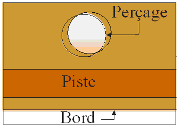
Figure 1087: Misregistration of top and bottom coverlay
| ||||
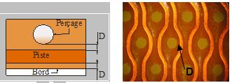
Table 1053: Sculptured flex - aspect of coverlay
|
Ref.
|
Technological feature
|
Acceptance criteria
|
Procurement inspection sample
|
Measurement method
|
|
a.
|
Scratches, folding marks, blistering, nicks, contamination, voids, white spots
|
Target condition of coverlay is without defect. An incidental defect is acceptable in accordance with the criteria specified hereunder.
|
Location: PCB
|
Visual inspection magnification ≥ 10x
|
|
b.
|
Scratches, cuts
|
Accepted if superficial scratch
| ||
|
c.
|
Folding marks
|
Accepted if remaining insulation distance is in conformance with PCB definition dossier.
| ||
|
d.
|
Blistering (bubbles)
|
not acceptable
| ||
|
e
|
Delamination
|
not acceptable
| ||
|
f.
|
Nicks and tears
|
≤ 50 % of the insulation between edge of flex section to pattern
| ||
|
g.
|
Voids or pinhole in coverlay
|
Voids or pinholes are acceptable in case:
| ||
|
h.
|
Black spot contamination below coverlay
|
Not acceptable
| ||
|
i.
|
Fibre contamination below coverlay
|
acceptable if remaining insulation distance in conformance with PCB definition dossier
| ||
|
j.
|
Voids in adhesive
|
Incidental voids of ≤ 80 µm are acceptable in case the insulation distance is in conformance with the PCB definition dossier
| ||
|
k.
|
White spots below coverlay
|
Accepted if:
| ||
|
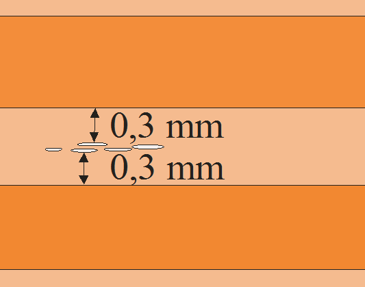
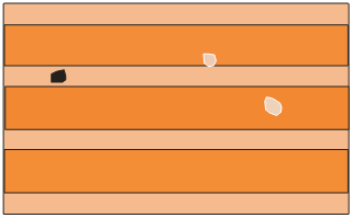
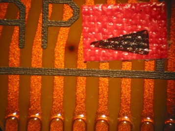 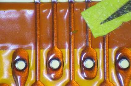   Figure 1089: Examples of white spot configurations and black spot contamination
| ||||

Table 1054: Sculptured flex - SnPb infiltration
|
Ref.
|
Technological feature
|
Acceptance criteria
|
Procurement inspection sample
|
Measurement method
|
|
a.
|
SnPb infiltration below coverlay
|
Not acceptable
|
Location: PCB
|
Visual inspection magnification ≥ 10x
|
|
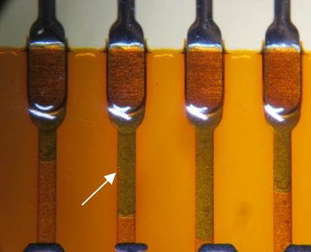
Figure 1091: Examples of SnPb infiltration on sculptured pad (left) and on tracks (right) | ||||
Table 1055: Sculptured flex - bare copper on fingers and pads
|
Ref.
|
Technological feature
|
Acceptance criteria
|
Procurement inspection sample
|
Measurement method
|
|
a.
|
Bare copper on fingers and pads
|
Not acceptable
|
Location: PCB
|
Visual inspection magnification ≥ 10x
|
|
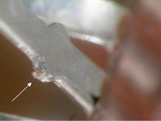
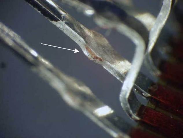
Figure 1092: Bare copper on fingers | ||||
Table 1056: Sculptured flex – misregistration between pads
|
Ref.
|
technological feature
|
Acceptance criteria
|
Procurement inspection sample
|
Measurement method
|
|
a.
|
Misregistration between top and bottom pads
|
Acceptable if
|
Location: PCB
|
Visual inspection magnification ≥ 10x
|
|
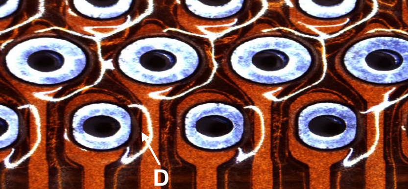
Figure 1093: Misregistration of pads | ||||
Table 1057: Sculptured flex – annular ring
|
Ref.
|
Technological feature
|
Acceptance criteria
|
Procurement inspection sample
|
Measurement method
|
|
a.
|
Annular ring on oblong pad on solder side
|
≥ 150 µm on smallest side
|
Location: PCB
|
Visual inspection magnification ≥ 10x
|
|
b.
|
Annular ring on circular pad on solder side
|
≥ 250 µm
| ||
|
c.
|
Annular ring on component side
|
Tangency acceptable in case no adhesive inside the hole, in conformance with 8.7.5e of ECSS-Q-ST-70-12
| ||
|
Figure 1094: Hole misregistration causing reduced annular ring | ||||
Table 1058: Sculptured flex - copper conductor width and spacing
|
Ref.
|
Technological feature
|
Acceptance criteria
|
Procurement inspection sample
|
Measurement method
| |
|
a.
|
Nicks, peaks and pinholes on conductors
|
Acceptable if all the following are met
|
Location: PCB
|
Visual inspection magnification ≥ 10x
| |
|
b.
|
Peaks and copper residue
|
Acceptable if
| |||
|
c.
|
Copper residue to the edge of the flex
|
Acceptable if insulation distance D ≥ 400µm between residue and edge of flex
| |||
|
d.
|
Bump on conductor due to local insufficient etching
|
Acceptable
| |||
|
e.
|
Conductor width and spacing
|
Tolerance of conductor width and spacing is ≤ 20 % in conformance with Table 7-3 from ECSS-Q-ST-70-12
| |||
|
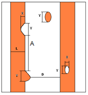
Figure 1095: Schematic of conductor width and spacing and local defects |
X: width of defect
| ||||
|
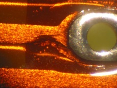
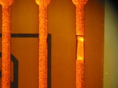
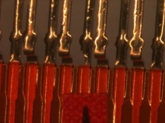
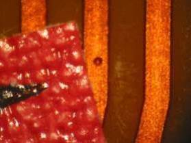
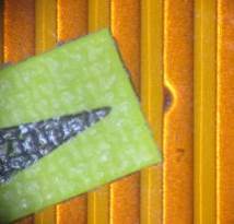
Figure 1096: Examples of nick near pad, nick on conductor, overetching reducing thickness of conductor, nick on finger, pinhole and local reduced track width (left to right)
| |||||
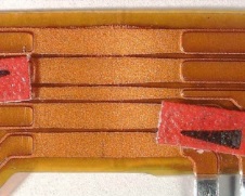


Table 1059: Adhesive in plated holes
|
Ref.
|
Technological feature
|
Acceptance criteria
|
Procurement inspection sample
|
Measurement method
| ||||||
|
a.
|
Adhesive in plated holes
|
Acceptable if hole diameter is in conformance with PCB definition dossier
|
Location: PCB
|
Visual inspection magnification ≥ 10x
| ||||||
Figure 1098: Adhesive in plated holes
| ||||||||||

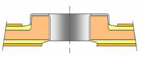

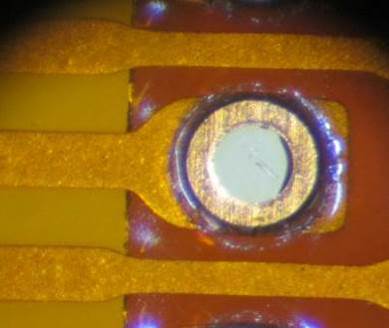
Table 1060: Sculptured flex – aspect of pads on solder side
|
Ref.
|
Technological feature
|
Acceptance criteria
|
Procurement inspection sample
|
Measurement method
| ||||||
|
a.
|
Absence of SnPb on pads;
|
Remaining circular pad width ≥ 250 µm
|
Location: PCB
|
Visual inspection magnification ≥ 10x
| ||||||
|
Remaining pad width on smallest side of oblong pad ≥ 150 µm
| ||||||||||
Figure 10100: SnPb coverage on pads
| ||||||||||

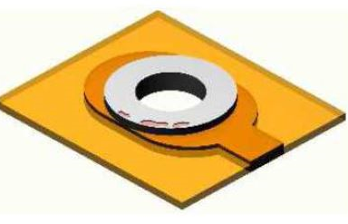
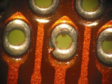
Table 1061: Sculptured flex - copper wrinkle
|
Ref.
|
technological feature
|
Acceptance criteria
|
Procurement inspection sample
|
Measurement method
|
|
a.
|
Copper wrinkle
|
Not acceptable
|
Location: PCB
|
Visual inspection magnification ≥ 10x
|
|
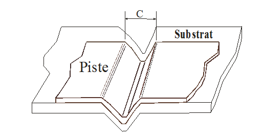
Figure 10102: Copper wrinkle | ||||
Table 1062: Sculptured flex – aspect of mechanical holes and edge of coverlay
|
Ref.
|
Technological feature
|
Acceptance criteria
|
Procurement inspection sample
|
Measurement method
| |
|
a.
|
nick, burr, tear in mechanical hole in coverlay or on edge of coverlay
|
Tear not acceptable.
|
Location: PCB
|
Visual inspection magnification ≥ 10x
| |
|
b.
|
Target condition: no burrs
| ||||
|
c.
|
Target condition: no nicks
| ||||
|

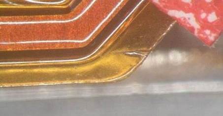
Figure 10103: Tear in hole and edge of coverlay | |||||
|
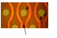
Figure 10104: Burrs on holes |
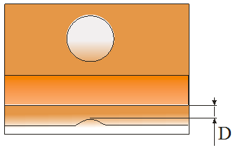
Figure 10105: Nick on edge of coverlay | ||||
Table 1063: Sculptured flex – scratch on coverlay
|
Ref.
|
Technological feature
|
Acceptance criteria
|
Procurement inspection sample
|
Measurement method
|
|
a.
|
Scratches, cuts
|
Accepted if superficial scratch
|
Location: PCB
|
Visual inspection magnification ≥ 10x
|
|
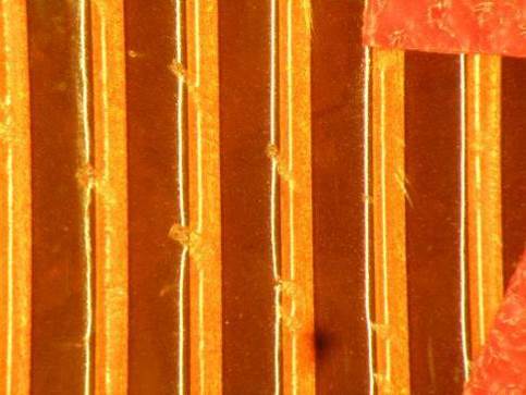
Figure 10106: Coverlay scratch – Non acceptable | ||||
Table 1064: Sculptured flex - aspect of finger after bending
|
Ref.
|
Technological feature
|
Acceptance criteria
|
Procurement inspection sample
|
Measurement method
|
|
a.
|
Aspect of finger after bending and SnPb coverage
|
Exposed copper not acceptable
|
Location: PCB
|
Visual inspection magnification ≥ 10x
|
|
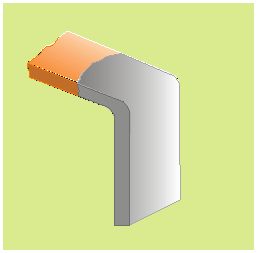
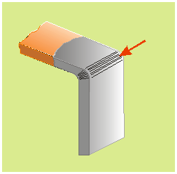
Figure 10107: Acceptable aspect of finger after bending
| ||||

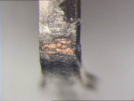
Table 1065: Sculptured flex - marking adhesion strength
|
Ref.
|
Technological feature
|
Acceptance criteria
|
Procurement inspection sample
|
Measurement method
|
|
a.
|
Marking adhesion strength
|
No lift of marking
|
Location: PCB
|
See clause 9.4.5
|
Table 1066: Sculptured flex - microsection
|
Ref.
|
Technological feature
|
Acceptance criteria
|
Procurement inspection sample
|
Measurement method
|
|
a.
|
Bulk Copper Thickness
|
As per PCB definition dossier with a tolerance of ± 25 µm
|
Location: coupon
|
See clause 9.4.5
|
|
b.
|
Copper Conductor Thickness
|
As per PCB definition dossier with a tolerance of ± 25 µm
| ||
|
c.
|
Kapton Base and Coverlay Thickness
|
25 µm ± 5µm
| ||
|
d.
|
Overall Assembly Thickness (No Conductor)
|
Calculated
| ||
|
e.
|
Overall Assembly Thickness (With Conductor)
|
Calculated
| ||
|
f.
|
Tin-Lead Thickness on Surface
|
7 µm minimum
| ||
|
g.
|
Tin-Lead Thickness in Hole
|
5 µm minimum
| ||
|
h.
|
Tin-Lead Thickness on Corners
|
1 µm minimum
| ||
|
“Calculated” indicates the addition of individual elements of the build-up.
| ||||
|
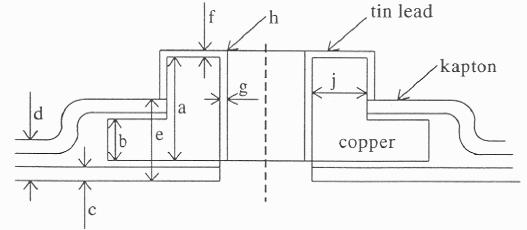
Figure 10109: Cross-section of hole: Copper conductor shown | ||||
|
Note: Ref. d. and e. have been derived to ensure full encapsulation of conductors and total air exclusion from the bond interface by the allowance of use of additional thickness of acrylic adhesive applied on a case by case basis dependent on circuit.
| ||||
Additional requirement to the tables
Annular ring
Annular ring shall be measured excluding the copper plating, except in the case of requirement 10.6.1b.
Annular ring on external layers shall be measured including the Cu plating.
The measurement method for annular ring is indicated in Table 101 and Table 102. The reason to include Cu plating in annular ring measurement on external pads is to enable annular ring measurement by visual inspection, whereas the other type of annular ring measurements are performed using microsectioning.
On layers without non-functional pad, the distance between the hole wall and the adjacent circuitry shall be in conformance with requirement 13.8.2g from ECSS-Q-ST-70-12.
This limits the misregistration of that layer, which cannot be measured without the presence of a pad.
The internal annular ring may be ≥ 25 µm provided that all the following conditions are met:
- it is in conformance with requirement 11.5.2a of ECSS-Q-ST-70-12;
- the panel includes registration coupons on all four corners for verification of annular ring in the full circumference.
- 1 The electrical coupon R from IPC-2221B allows for such verification. The IST coupon also includes a pattern for electrical registration. Alternatively the verification can be done by X-ray. Microscopic inspection of cross-sections only verifies in one direction and does not assess the full circumference.
- 2 Requirement 11.5.2a of ECSS-Q-ST-70-12 includes teardrop reinforcement and identification of the review item for the PCB definition dossier. The requirement is specified for HDI technology. Therefore a PCB without microvias falls within the HDI technology in case it uses reduced annular ring.
- 3 Table 106 and Table 1026 specify that cracks and wicking cannot be more than the minimum annular ring. Therefore wicking is limited to 25 µm in case such small annular ring is used.
- 4 This requirement is valid for rigid and flex laminate. Larger movement of flex layers causes higher tolerances for annular ring. Therefore the requirement of 50 µm is reduced to 25 µm. However, this margin cannot be used to justify a design with a smaller pad diameter. The pad diameter is designed as if the annular ring was 50 µm, in conformance with the requirement 7.5.2h from ECSS-Q-ST-70-12.
- 5 It is preferred to implement the electrical registration coupon on all corners of the panel, which is deemed a more efficient verification of annular ring compared to microsectioning on 2 opposite corners. To accommodate the recurrent designs without electrical registration coupons, the annular ring requirement of 50 µm is maintained for that technology.
Pad lift and associated laminate cracks
Pad lift shall not be acceptable except for the case specified in Table 1025.
In addition to the selected laminate material, the risk of pad lift further increases by the combination of thick PCBs with high layer count, small annular ring and a high amount of heat cycles representative of hand soldering, as performed by rework simulation. On technology prone to pad lift, it is good practice to design with large annular ring or to take other risk mitigations.
Cracks in the laminate underneath SMT pads without via-in-pad shall be evaluated as dielectric cracks, in conformance with the Table 1026.
SMT pads without via-in-pad are not included on coupons.
The height of the pad lift shall be in conformance with Table 1025.
The height of the pad lift shall include adhesive separation between pad and resin as well as cracks or voids due to cohesive separation inside the dielectric.
In case cohesive or adhesive separations are not clearly identifiable, the angle of the pad may be used to calculate the height of the pad lift.
The parts of cracks or voids protruding from underneath the pad shall be evaluated as dielectric cracks in conformance with the Table 1026.
In case cracks associated with pad lift are observed on the coupon for procurement, conformance to Table 1025 shall be evaluated after group 6 test for representative technology and recorded in the PID.
This provides an evaluation that the cracks associated with pad lift do not propagate until the hole wall after group 6, as done for qualification. Propagation of cracks until the hole wall increases the risk of further propagation along the hole wall and potential rupture of innerlayer connections.
Cracks associated with pad lift shall not reach the hole wall before or after thermal stress.
The parts of cracks or voids underneath the pad associated with pad lift shall not reduce the insulation distance to adjacent circuitry below the values specified by the PCB definition dossier, in the DRD of ECSS-Q-ST-70-12 Annex A.
- 1 The insulation distance specified in the PCB definition dossier is in conformance with ECSS-Q-ST-70-12 Table 13-7.
- 2 It is good practice that technology prone to pad lift is designed with margin such that the potential pad lift does not reduce the insulation between component holes and adjacent circuitry.
Adjacent circuitry as specified in requirement 10.6.2i shall include the worst-case in the PCB.
In case tracks are routed in the PCB on layer 2 or layer N-1 underneath the external pad that can show pad lift or associated cracks, it is important to represent this in the coupon in conformance with requirement 15.2a from ECSS-Q-ST-70-12. In case such design is not represented on the coupon, the potential crack on the coupon cannot easily be assessed by the PCB manufacturer for its remaining insulation distance to adjacent circuitry. In this case, it is important to perform FAI in conformance with requirement 15.2b from ECSS-Q-ST-70-12 and to include the theoretical worst-case adjacent circuitry of the PCB in the assessment from requirement 10.6.2j.
A specific evaluation of possible anomalies of materials or processes shall be performed by the PCB manufacturer in case pad lift and associated cracks are observed on polyimide PCBs.
- 1 This is specified because polyimide PCB have high Tg and are considered robust to thermal stress. Therefore it is not expected to see this defect and it can be an indicator of a process or material anomaly.
- 2 Polyimide rigid-flex PCBs that use many layers of no-flow prepreg can be prone to pad lift due to high thermal expansion in Z-direction and low Tg of the material. Alternative processes or materials can be investigated with the PCB manufacturer to avoid pad lift.
Miscellaneous
Any defects that are specified within ECSS-Q-ST-70-60 to be acceptable after group 6, shall also be acceptable after group 4.
The plating in microvias shall be evaluated in conformance with Table 1011 in high density and low density footprint.
Microvias in low density footprint are included in coupons from set 1 and set 2. Microvias in high density footprint are included in the IST coupon, which can be microsectioned after IST test.
In case cracks are observed in microsections for procurement in conformance with Table 1026 within the dimensional limitation specified for Ref. b and Ref. c, a referee test shall be performed by taking 4 additional microsections from a spare PCB from the same batch and by evaluation of conformance to Table 1026.
Remaining insulation distance shall be the sum of insulation distances to conductors that are not affected by cracks.
Insulation from crack to adjacent conductor of less than 20 μm shall not be included in the calculation of remaining insulation distance for Ref. g from Table 1026.
This is specified because cracks closer than 20 μm to a conductor are at risk to be in contact with the conductor out-of-plane from the microsection. In case the crack is further separated from adjacent conductors than 20 μm, the remaining insulation distance can be calculated by addition of the insulation on both sides of the crack to adjacent conductors. An example is shown in Figure 10110, which is a zoom from Figure 1047. In case both a) and b) are > 20 μm, the remaining insulation distance equals c) minus the length of the crack. In case a) is < 20 μm, the remaining insulation distance equals b).
 Figure 10110: Calculation of remaining insulation distance
PTH with a diameter of ≥ 0,6 mm shall meet the requirement for finished hole diameter from the PCB definition dossier.
These hole diameters cannot be reduced by a bulb of SnPb.
Plated holes with a diameter < 0,6 mm may have a reduced diameter due to blocking with SnPb.
In some applications, such as for nano-D connectors, PTH are used with a diameter < 0,6 mm with SnPb surface finish. In this case it is important to review the finished hole diameter. It is the responsibility of the PCB manufacturer in case such design is specified in the PCB definition dossier and accepted in the MRR, in which case it is good practice to raise it as a review item. Blocking with SnPb can also be a review item for larger hole diameters.
Coverlay and its adhesive may partly cover the pad of flexible PCBs in case the annular ring is in conformance with clause 8.5.1 from ECSS-Q-ST-70-12 and Ref. d from Table 102.
Minimum annular ring is 250 µm on a component hole and 100 µm on a non-soldering hole.
The customer may specify a requirement for maximum copper thickness in the PCB definition dossier.
ECSS-Q-ST-70-60 and ECSS-Q-ST-70-12 do not specify a maximum copper thickness for plated layers. This could be important for HDI layers, thermal performance of PCBs or for RF applications. Copper thickness on plated layers (internal/external) can be influenced by pattern design and value above maximum are acceptable in case all other requirements like dielectric thickness, undercut, conductor width/space are achieved.
In case of overhang of Au or Ni/Au in conformance with Table 1015, the assembled PCB shall be conformal coated.
Overhang occurs when Au or Ni/Au is plated before etching. To avoid overhang, the plating can occur after etching, in which case the circuit to be plated is designed to enable electrical connection. Brushing of overhang is not allowed in conformance with requirement 6.10.2n and its note. Other surface finishes, such as ENEPIG, are available that do not cause any overhang. This is necessary on RF PCBs in case conformal coating is not desired.
ANNEX(normative)Qualification letter – DRD
DRD identification
Requirement identification and source document
This DRD is called from ECSS-Q-ST-70-60, requirement 5.12a.
Purpose and objective
The purpose of the DRD is to describe the content of the qualification letter.
Expected response
Scope and content
The qualification letter shall contain the following:
- Date of issue;
- Contact details of PCB manufacturer and qualification authority;
- Reference to request of qualification;
- Reference to evaluation test report;
- Reference to audit report;
- Reference to qualification test report;
- Qualified technology;
- PID reference;
- Qualification period.
Special remarks
None.
ANNEX(normative)CoC for PCB – DRD
DRD identification
Requirement identification and source document
This DRD is called from ECSS-Q-ST-70-60, requirement 8.3a.
Purpose and objective
The purpose of the DRD is to describe the content of the CoC and its lab reports.
Expected response
Scope and content
CoC for PCB
The CoC shall contain the following:
- Declaration of conformance, in conformance with B.2.1.2;
- Lab report for visual inspection of PCBs for qualitative aspects, in conformance with B.2.1.3;
- Lab report for visual inspection of PCBs for dimensional verification, in conformance with B.2.1.4;
- Lab report for microsection of coupons for qualitative aspects, in conformance with B.2.1.5;
- Lab report for microsection of coupons for dimensional verification, in conformance with B.2.1.6;
- Lab report for additional tests, in conformance with B.2.1.7.
The CoC shall cover the batch or a subset.
The CoC shall record the presence of the following: - Microvia plating voids in conformance with Table 1011;
- Voids or cracks in the resin of blind and buried vias inside zone A in conformance with Table 1017;
- Dimple in blind via in conformance with Table 1019;
- Voids and inclusions in copper plating and skip plating in conformance with Table 1021;
- Resin voids in conformance with Table 1023;
- Pad lift and cracks associated with pad lift in conformance with Table 1025;
- Dielectric cracks in conformance with Table 1026;
- Separation between external copper foil and copper plating in conformance with Table 1027;
- Smear in conformance with Table 1029;
- Hole wall pull away or resin recession in conformance with Table 1030;
- Swirl or milky appearance in no flow prepreg and demarcation line in no flow prepreg and dotted interface line in conformance with Table 1033;
- Non-metallic contamination in microsection in conformance with Table 1034;
- Adhesive voids in rigid-flex interface in conformance with Table 1036;
- Non-metallic contamination or inhomogeneity in conformance with Table 1042;
- Scratches on conductor and scratches on dielectric in conformance with Table 1043;
- Granular aspect in tin-lead in conformance with Table 1046;
- Fibre protrusion in conformance with Table 1049;
- Aspect of flex laminate and coverlay in conformance with Table 1051;
- Aspect of coverlay for sculptured flex in conformance with Table 1053;
- Aspect of mechanical holes and edge of coverlay for sculptured flex in conformance with Table 1062;
- Scratch of coverlay for sculptured flex in conformance with Table 1063.
- 1 This is recorded in the CoC even if it is in conformance with the requirements from the tables to provide traceability. See column “present?” in Table B-2, Table B-4 and Table B-5. More details can be specified in the “comments” field of the tables.
- 2 For example, this is important for KIP/MIP after assembly to ensure that blistering or voids in coverlay adhesive did not propagate.
Declaration of conformance
The declaration of conformance shall include the following:
- Declaration of conformance to ECSS-Q-ST-70-60;
- Declaration of conformance to the PCB definition dossier;
- Traceability reference to the PCB definition dossier from procurement authority including revision and issue number;
- MRR reference;
- In case of partial or noncompliance to B.2.1.2a1 or B.2.1.2a2 reference to waiver request;
- Purchase order number from procurement authority;
- Traceability reference from PCB manufacturer;
- Date code, as per the following format: YYWW;
- Quantity of delivered PCBs in the batch;
- Serial numbers of delivered PCBs in the batch;
- Signature from PCB manufacturer.
- 1 Note to item 3: This traceability reference can be named ‘part number’.
- 2: Note to item 7: This traceability reference can be named ‘batch code’.
- 3 Note to item 8: YYWW indicates a two digit reference to year followed by a two digit reference to week number.
Lab report for visual inspection of PCBs for qualitative aspects
Lab report for visual inspection of PCBs for qualitative aspects shall include the following:
- Arbitrary defects of conductors and pads (mouse bites, dents, nicks, pinhole, unintentional pattern) in conformance with Table 1038 and Table 1039;
- Lifting of conductor pattern in conformance with Table 1040;
- Copper or nickel visible on top surfaces in conformance with Table 1040;
- Corrosion of copper in conformance with Table 1040;
- Blistering or air bubbles in conformance with Table 1041;
- Delamination in conformance with Table 1041;
- Crazing and measling in conformance with Table 1041;
- Surface contamination or inclusion of foreign matter in conformance with Table 1042;
- Non-homogeneous colour of innerlayer copper in conformance with Table 1042;
- Scratches in conformance with Table 1043;
- Weave exposure in conformance with Table 1044;
- Haloing in conformance with Table 1045;
- SnPb surface quality in conformance with Table 1046;
- Marking in conformance with Table 1047;
- Coverlay registration and annular ring of terminations on flexible PCB in conformance with Ref. d from Table 102;
- Rigid-to-flex interface, alignment of prepreg in conformance with Table 1048;
- Rigid-to-flex interface, fibre protrusion in conformance with Table 1049;
- Rigid-to-flex interface, haloing in conformance with Table 1050;
- Rigid-to-flex interface, aspect of flex laminate and coverlay in conformance with Table 1051.
The visual inspection of qualitative aspects shall include the review items from the MRR.
The acceptance criteria for visual inspection for qualitative aspects shall cover all PCBs in the batch by providing a pass/fail evaluation.
Inspection and evaluation of requirements is performed on all PCBs in the batch, whereas the reporting provides a summary.
Lab report for visual inspection of PCBs for dimensional verification
The sampling plan for performing visual inspection of PCBs for dimensional aspects shall be as specified in Table 81.
The lab report for visual inspection for dimensional verification shall include the following:
- the PCB thickness is a representative measurement;
- the PCB length and width are representative measurements;
- specific dimensional features from the PCB definition dossier are representative measurements;
- the warp and twist are the maximum measurements recorded on the worst-case PCB;
- diameter of plated and non-plated holes for all diameters is a pass/fail evaluation, except for < 0,6mm holes with SnPb in conformance with 10.6.3g;
- external annular ring for all plated-hole types is a pass/fail evaluation;
- external conductor width and spacing is a pass/fail evaluation for minimum width and spacing;
- comparison of lay-out to the drawing for the presence of plated and non-plated holes and milling is a pass/fail evaluation.
- 1 Comparison of lay-out to the drawing is performed as in-process inspection in conformance with 6.3g.
- 2 Pass/fail evaluations provide an assessment of dimensions with respect to their tolerances specified in the PCB definition dossier.
- 3 In case an external conductor is indicated as critical in the PCB definition dossier it can be inspected on all PCBs.
- 4 Specific dimensional features can include cut-out or radius of PCB edge.
Lab report for microsection of coupons for qualitative aspects
The lab report for microsection for qualitative aspects shall include the following:
- Via filling in conformance with Table 1017;
- Cap lift and planarity in conformance with Table 1018 and Table 1019;
- Burrs and nodules in conformance with Table 1020;
- Voids or inclusions in copper plating in conformance with Table 1021;
- Wedge voids in conformance with Table 1022;
- Resin voids in conformance with Table 1023;
- Delamination, blistering, crazing, measling in conformance with Table 1024;
- Pad lift in conformance with Table 1025;
- Dielectric cracks in conformance with Table 1026;
- Cracks and separation in copper in conformance with Table 1027;
- ICD in conformance with Table 1028;
- Smear in conformance with Table 1029;
- HWPA and resin recession in conformance with Table 1030;
- Nail heading in conformance with Table 1031;
- CIC in conformance with Table 1032;
- Inhomogeneity in dielectric in conformance with Table 1033;
- Contamination or inclusion in conformance with Table 1034;
- Delamination between coverlay and prepreg in conformance with Table 1035;
- Adhesive voids in coverlay and bond-ply in conformance with Table 1036;
- Misalignment of prepreg in rigid-flex-interface in conformance with Table 1037.
The lab report for microsection for qualitative aspects shall include the review items from the MRR.
The acceptance criteria for microsection for qualitative aspects shall cover all microsections of coupons in the batch by providing a pass/fail evaluation.
Inspection and evaluation of requirements is performed on all microsections of coupons in the batch, whereas the reporting provides a summary.
The lab report for microsection for qualitative aspects shall include the following representative pictures of microsections covering the batch, except in case this is specifically waived by the customer in the PCB definition dossier:
- Overview of PTH after SB in dark field showing laminate integrity, build-up;
- 500x magnification after SB in bright field showing interconnect and absence of ICD;
- 500x magnification as received in bright field showing SnPb on corner;
- Overview of rigid-to-flex interface after SB in dark field showing laminate integrity and absence of delamination.
Lab report for microsection of coupons for dimensional verification
The microsection of coupons for dimensional verification shall be performed for all panels.
The summary in the lab report shall be for a representative measurement covering all panels.
The lab report for visual inspection for dimensional verification shall include the following:
- Annular ring internal and external in conformance with Table 101 and Table 102;
- Copper foil thickness in conformance with Table 103;
- Copper plating thickness in conformance with Table 104;
- Etchback in conformance with Table 105;
- Wicking in conformance with Table 106;
- Wrap copper in conformance with Table 107;
- Dielectric thickness in conformance with Table 108 and Table 109;
- Microvias dimensions and plating voids in conformance with Table 1010 and Table 1011;
- SnPb thickness in conformance with Table 1012;
- Electrolytic Ni and Au dimensions in conformance with Table 1013;
- Undercut and overhang in conformance with Table 1014 and Table 1015;
- Dimensions of rigid-flex-interface in conformance with Table 1016.
Additional tests
The lab report for additional tests shall include the following:
- Solderability in conformance with 9.4.11 in case this is applicable as specified in Table 1012;
- High resistance electrical test and continuity test in conformance with 9.3.7.2 and 9.3.8, including serial numbers of accepted PCBs;
- IST in conformance with 9.5.5.
Special remarks
The example test reports in Table B-1 to Table B-7 can be used.
Table: Example of a declaration of conformance
|
Declaration of Conformance:
| |
|
□ In conformance with ECSS-Q-ST-70-60
| |
|
□ In conformance with PCB definition dossier
| |
|
Reference to waiver request, if applicable:
| |
|
MRR reference:
| |
|
Report reference number:
| |
|
Issue date of report:
| |
|
Purchase order:
|
|
|
PCB Manufacturer & location:
|
|
|
Customer Part Number
|
|
|
PCB definition dossier and issue nr
|
|
|
Batch code from PCB manufacturer
|
|
|
Date code of PCB manufacture (YYWW)
|
|
|
Serial number (S/N):
|
|
|
Quantity ordered
|
|
|
Quantity delivered
|
|
|
Signature
|
|
Table: Example of a lab report for visual inspection of PCBs for qualitative aspects
|
Lab report for visual inspection of PCBs for qualitative aspects
|
Sampling
|
Requirement references
|
Value
|
Pass/Fail
|
Present? as per B.2.1.1c
|
|
Arbitrary defects of conductors, and pads (mouse bites, dents, nicks, pinhole, unintentional pattern)
|
100%
|
Table 1038 + Table 1039
|
- |
|
- |
|
Lifting of conductor pattern
|
100%
|
Table 1040
|
- |
|
- |
|
Copper or nickel visible on top surface
|
100%
|
Table 1040
|
- |
|
- |
|
Corrosion of copper
|
100%
|
Table 1040
|
- |
|
- |
|
Blistering or air bubbles
|
100%
|
Table 1041
|
- |
|
- |
|
Delamination
|
100%
|
Table 1041
|
- |
|
- |
|
Crazing and measling
|
100%
|
Table 1041
|
- |
|
- |
|
Surface contamination or inclusion of foreign matter
|
100%
|
Table 1042
|
- |
|
- |
|
Non-homogeneous colour (oxidation of innerlayer copper, white spots )
|
100%
|
Table 1042
|
- |
|
|
|
Scratches
|
100%
|
Table 1043
|
- |
|
|
|
Weave exposure
|
100%
|
Table 1044
|
- |
|
- |
|
Haloing
|
100%
|
Table 1045
|
- |
|
- |
|
SnPb surface quality
|
100%
|
Table 1046
|
- |
|
|
|
Marking
|
100%
|
Table 1047
|
- |
|
- |
|
Coverlay registration and annular ring of terminations on flexible PCB
|
100%
|
Table 102
|
- |
|
- |
|
Rigid-to-flex interface, alignment of prepreg
|
100%
|
Table 1048
|
- |
|
- |
|
Rigid-to-flex interface, fibre protrusion
|
100%
|
Table 1049
|
- |
|
|
|
Rigid-to-flex interface, haloing
|
100%
|
Table 1050
|
- |
|
- |
|
Rigid-to-flex interface, aspect of flex laminate and coverlay
|
100%
|
Table 1051
|
- |
|
|
|
Review items from MRR
|
100%
|
B.2.1.3b
|
- |
|
- |
|
Comments:
| |||||
Table: Example of a lab report for visual inspection of PCBs for dimensional verification
|
Lab report for visual inspection of PCBs for dimensional verification
|
Sampling 1 PCB/panel
|
Requirement references
|
Value
|
Pass/Fail
|
|
PCB thickness, □over laminate, □ over surface finish
|
s/n:
|
9.3.3.1b
|
|
|
|
|
Sampling 1 PCB/batch
|
Requirement references
|
Value
|
Pass/Fail
|
|
PCB length
|
s/n:
|
9.3.3.1c
|
|
|
|
PCB width
|
s/n:
|
9.3.3.1c
|
|
|
|
specific dimensional features from the PCB definition dossier (e.g. cut-out, radius)
|
|
B.2.1.4b3
|
|
|
|
Warp and twist (maximum measurements recorded on the worst-case PCB)
|
s/n:
|
9.3.3.2-9.3.3.3
|
|
|
|
Diameter of plated and non-plated holes for all diameters ≥0,6mm
|
s/n:
|
9.3.3.1d
|
-
|
|
|
Diameter of plated holes <0,6mm if specified in PCB definition dossier
|
100%
|
10.6.3g
|
-
|
|
|
External annular ring for all plated-hole types
|
s/n:
|
10.6.1b
|
-
|
|
|
External conductor width and spacing on minimum dimensions
|
s/n:
|
9.3.3.1g, 9.3.3.1h, 9.3.3.1i,
|
-
|
|
|
External conductor width and spacing fine pitch on minimum dimensions
|
100%
|
9.3.3.1g, 9.3.3.1h, 9.3.3.1i,
|
-
|
|
|
Comparison of lay-out to the drawing (presence of plated and non-plated holes and milling)
|
s/n:
|
6.3g
|
-
|
|
|
Comments:
| ||||
Table: Example of a Lab report for microsection of coupons for qualitative aspects
|
Lab report for microsection of coupons for qualitative aspects
|
Inspection
|
Requirement references
|
as per flow from Figure 81
| |
|
Pass/Fail
|
Present? as per B.2.1.1c
| |||
|
Via filling, voids or cracks
|
each panel
|
Table 1017
|
|
|
|
Cap lift
|
each panel
|
Table 1018
|
|
-
|
|
Planarity, dimple
|
each panel
|
Table 1019
|
|
|
|
Burrs and nodules
|
each panel
|
Table 1020
|
|
-
|
|
Voids in copper plating
|
each panel
|
Table 1021
|
|
|
|
Wedge voids
|
each panel
|
Table 1022
|
|
-
|
|
Resin voids
|
each panel
|
Table 1023
|
|
|
|
Delamination, blistering, crazing, measling
|
each panel
|
Table 1024
|
|
-
|
|
Pad lift
|
each panel
|
Table 1025
|
|
|
|
Dielectric cracks
|
each panel
|
Table 1026
|
|
|
|
Cracks and separation in copper
|
each panel
|
Table 1027
|
|
|
|
ICD
|
each panel
|
Table 1028 + Table 1010 Ref. e
|
|
-
|
|
Smear
|
each panel
|
Table 1029
|
|
|
|
HWPA and resin recession
|
each panel
|
Table 1030
|
|
|
|
Nail heading
|
each panel
|
Table 1031
|
|
-
|
|
CIC
|
each panel
|
Table 1032
|
|
-
|
|
Inhomogeneity in dielectric
|
each panel
|
Table 1033
|
|
|
|
Contamination or inclusion
|
each panel
|
Table 1034
|
|
|
|
Delamination between coverlay and prepreg
|
each panel
|
Table 1035
|
|
-
|
|
Adhesive voids in coverlay and bond-ply
|
each panel
|
Table 1036
|
|
|
|
Misalignment of prepreg in rigid-flex-interface
|
each panel
|
Table 1037
|
|
-
|
|
Review items from MRR
|
each panel
|
B.2.1.5b
|
|
-
|
|
Comments:
| ||||
|
Pictures of microsections in conformance with B.2.1.5d.
| ||||
Table: Example of a lab report for microsection of coupons for dimensional verification
|
Lab report for microsection of coupons for dimensional verification
|
Requirementreferences
|
Pass/Fail
|
Present?as per B.2.1.1c
|
|
Requirementreferences
|
Measured value
|
|
covers 100%
|
measure 1 per batch
| |||||
|
Annular ring internal
|
Table 101
|
|
-
|
s/n:
|
50 μm
|
|
|
Annular ring internal reduced
|
Table 101
|
|
-
|
s/n:
|
Ref. e, 25 μm
|
|
|
Annular ring microvia capture pad
|
Table 101
|
|
-
|
s/n:
|
Ref. d, 10 μm
|
|
|
Annular ring external blind via
|
Table 102
|
|
-
|
s/n:
|
Ref. e, 100 μm
|
|
|
Annular ring external microvia
|
Table 102
|
|
-
|
s/n:
|
Ref. f, 10 μm
|
|
|
Copper foil thickness
|
Table 103
|
|
-
|
s/n:
|
|
build-up report
|
|
Copper plating thickness, PTH and via
|
Table 104
|
|
-
|
s/n:
|
Ref. a, b, c
|
|
|
Copper plating thickness, blind and buried via
|
Table 104
|
|
-
|
s/n:
|
Ref. d
|
|
|
Etchback
|
Table 105
|
|
-
|
s/n:
|
Ref. a
|
|
|
Wicking
|
Table 106
|
|
-
|
s/n:
|
|
|
|
Wrap copper
|
Table 107
|
|
-
|
s/n:
|
|
|
|
Dielectric thickness
|
Table 108 + Table 109
|
|
-
|
s/n:
|
|
build-up report
|
|
Dielectric thickness - number of prepreg
|
Table 108 + Table 109
|
|
-
|
s/n:
|
Ref. b
|
|
|
Microvias dimple and bump
|
Table 1010
|
|
-
|
s/n:
|
Ref. a, b
|
|
|
Microvias aspect ratio
|
Table 1010
|
|
-
|
s/n:
|
Ref. c
|
|
|
Microvias diameter to capture pad
|
Table 1010
|
|
-
|
s/n:
|
Ref. d
|
|
|
Microvias plating voids
|
Table 1011
|
|
|
s/n:
|
|
|
|
SnPb thickness PTH hole wall
|
Table 1012
|
|
-
|
s/n:
|
Ref. c
|
|
|
SnPb thickness PTH corner
|
Table 1012
|
|
-
|
s/n:
|
Ref. d
|
|
|
SnPb thickness PTH pads
|
Table 1012
|
|
-
|
s/n:
|
Ref. e
|
|
|
Electrolytic Ni
|
Table 1013
|
|
-
|
s/n:
|
Ref. a
|
|
|
Electrolytic Au
|
Table 1013
|
|
-
|
s/n:
|
Ref. b, c
|
|
|
Undercut
|
Table 1014
|
|
-
|
s/n:
|
|
|
|
Overhang
|
Table 1015
|
|
-
|
s/n:
|
Ref. b
|
|
|
Dimensions of rigid-flex-interface
|
Table 1016
|
|
-
|
s/n:
|
Ref. a, b
|
|
|
Comments:
| ||||||
Table: Example of a build-up report
|
Layer
|
Layer stacking
|
Thickness requirements
|
Measured value (µm)on s/n: ………..
|
Pass / Fail
| ||
|
Nominal (µm)
|
Tolerances (µm)
| |||||
|
min
|
max
| |||||
|
1 |
copper |
|
|
|
|
|
|
|
dielectric |
|
|
|
|
|
|
2 |
|
|
|
|
|
|
|
|
|
|
|
|
|
|
|
3 |
|
|
|
|
|
|
|
|
|
|
|
|
|
|
|
4 |
|
|
|
|
|
|
|
|
|
|
|
|
|
|
|
5 |
|
|
|
|
|
|
|
|
|
|
|
|
|
|
|
6 |
|
|
|
|
|
|
|
|
|
|
|
|
|
|
|
7 |
|
|
|
|
|
|
|
|
|
|
|
|
|
|
|
8 |
|
|
|
|
|
|
|
|
|
|
|
|
|
|
|
9 |
|
|
|
|
|
|
|
|
|
|
|
|
|
|
|
10 |
|
|
|
|
|
|
|
|
|
|
|
|
|
|
|
11 |
|
|
|
|
|
|
|
|
|
|
|
|
|
|
|
12 |
|
|
|
|
|
|
|
|
|
|
|
|
|
|
|
13 |
|
|
|
|
|
|
|
|
|
|
|
|
|
|
|
14 |
|
|
|
|
|
|
|
|
|
|
|
|
|
|
|
15 |
|
|
|
|
|
|
|
|
|
|
|
|
|
|
|
16 |
|
|
|
|
|
|
|
|
|
|
|
|
|
|
|
17 |
|
|
|
|
|
|
|
|
|
|
|
|
|
|
|
18 |
|
|
|
|
|
|
|
|
|
|
|
|
|
|
|
19 |
|
|
|
|
|
|
|
|
|
|
|
|
|
|
|
20 |
|
|
|
|
|
|
|
|
|
|
|
|
|
|
|
21 |
|
|
|
|
|
|
|
|
|
|
|
|
|
|
|
22 |
|
|
|
|
|
|
Table: Example of a lab report for additional tests
|
Lab report for additional tests
|
Pass
|
Fail
|
|
|||
|
Solderability
|
9.4.11
|
|
|
|
|
|
|
High resistance electrical test
|
9.3.7
|
|
|
list of s/n:
|
|
|
|
Continuity test
|
9.3.8
|
|
|
list of s/n:
|
|
|
|
IST
|
9.5.5
|
|
|
report reference:
|
|
|
|
Comments:
| ||||||
ANNEX(normative)Qualification test report – DRD
DRD identification
Requirement identification and source document
This DRD is called from ECSS-Q-ST-70-60 requirement 5.10c.
Purpose and objective
The purpose of the DRD is to describe the content of the qualification test report.
Expected response
Scope and content
The qualification test report shall include:
- Description and history of the samples.
- Reference to the approved qualification test plan.
- All results from the qualification tests in conformance with requirements from clause 7.2.
- Photographic documentation of results obtained from microsectioning. The photographic documentation of microsections from the qualification test report shall use magnification level, lighting, micro-etchant and surface preparation in conformance with clauses 9.5.2 and 10.
Special remarks
The qualification test report shall be maintained under configuration control.
ANNEX(normative)Process Identification Document (PID) for PCB manufacturing – DRD
DRD identification
Requirement identification and source document
This DRD is called from ECSS-Q-ST-70-60 requirement 5.9c.1.
Purpose and objective
The purpose of the PID is to specify the manufacturing processes, materials and equipment of the qualified PCB technology. It also specifies the technological parameters of the qualified design.
The PID consist of a general part and specific parts. A general part of the PID describes the company, whereas specific parts of the PID describe each qualified technology.
Expected response
Scope and content
General part of the PID
The general part of the PID shall include the following information:
- Description of the company: history in business, products, staff, customers and the qualified site, in case of multiple sites;
- Technology road map;
- Organization chart with names and functions of key personnel;
- Quality certifications;
- Description of the process flow for order treatment, including the following:
- Design review in conformance with the clause 5.2 of ECSS-Q-ST-70-12;
- MRR in conformance with the clause 5.2 of ECSS-Q-ST-70-12;
- Outgoing inspection and CoC in conformance with the clause 8;
- List of main equipment for the production of PCBs, including type and brand name;
- List of test and control equipment with their capabilities;
- List of work instructions for manufacture and control of PCBs, with document numbers and issue references.
- 1 For D.2.1.1a.7, examples of test capabilities are metallographic examination, chemical analysis, failure analysis, mechanical and electrical test including functional testing of PCBs.
- 2 For D.2.1.1a.8, the work instructions include the process description.
Specific parts of the PID
Specific parts of the PID shall include:
- Manufacturing and quality control flow charts with reference to applicable work instructions;
- List of base materials and chemicals with brand name, type, and supplier;
- Production flowchart, including in-process inspections and reference to work instructions in conformance with D.2.1.1a8;
- Description of qualified domain in conformance with the items specified in requirement G.2.1b;
- Description of any review items that have been specifically qualified, as specified in clause <7>a of Annex A of ECSS-Q-ST-70-12;
- Subcontracted processes.
Special remarks
If several technologies are qualified, the general part of the PID may be a separate document to avoid duplication in the PIDs for each technology.
All PIDs shall have an identification of the issue, revision number and date, and a page showing the modifications introduced at each revision.
The modifications introduced since the previous revision of a PID shall be identified with specific marks or font.
It is good practice to include in the PID the following:
- in-process inspection as per 6.3f;
- approach for TMA as per 6.3h;
- etchback as per 6.3i;
- selection, test and inspection of prepreg, laminate, flex laminate, coverlay, bond-ply, copper foil, heat sinks and metal core as per 6.5g;
- repair operations as per 6.10.2a;
- specification of solderability test for procurement as per 8.2.4i;
- planarization and selective plating processes as per Table 107;
- group 6 evaluation of separation between hole wall and resin inside blind/buried via as per Table 1017 Ref. c;
- group 6 evaluation of separation between external copper foil and copper plating as per Table 1027 Ref. c;
- group 6 evaluation of >20% HWPA or RR as per Table 1030;
- evaluation of swirl or milky appearance as per Table 1033 Ref. c;
- evaluation of demarcation line as per Table 1033 Ref. d;
- evaluation of dotted interface line as per Table 1033 Ref. e;
- group 6 evaluation of pad lift and associated laminate cracks as per 10.6.2g and Table 1025;
- group 6 evaluation of interface lines between Cu plating as per the Note of Table 1027.
ANNEX(normative)Process change notice (PCN) – DRD
DRD identification
Requirement identification and source document
This DRD is called from ECSS-Q-ST-70-60, requirement 5.13f and F.2.1a.1.
Purpose and objective
The purpose of the DRD is to describe the content of the process change notice (PCN).
Expected response
Scope and content
Process changes shall include process parameters, chemistry, material, equipment, process flow and inspections.
The PCN shall contain the following:
- Categorisation of process change as “major” or “minor”;
- Justification for categorisation;
- Description of old and new process;
- Justification for change;
- Reference to work instruction in PID;
- In case of minor process change, results of verification tests and inspections;
- Request for major process change including qualification test plan;
- Request for approval of implementation of the major process change including qualification test report;
- Optional approval from procurement authority for major process change in conformance with requirement 5.13h.
Special remarks
None.
ANNEX(normative)QA report – DRD
DRD identification
Requirement identification and source document
This DRD is called from ECSS-Q-ST-70-60, requirement 5.14a.
Purpose and objective
The purpose of the DRD is to describe the content of the QA report.
Expected response
Scope and content
The QA report shall contain the following:
- Status of process changes, including associated process change notices in conformance with the DRD in Annex E;
- Overview of internal nonconformances, scrap, cause, yield and corrective action;
- Overview of external nonconformances, cause and corrective action;
- Overview of KPIs including OTD;
- Overview of planned and implemented investments;
- Changes in personnel and organigram;
- Overview of major visits by procurement authority, qualification authority or by certification bodies;
- Action list with status.
Special remarks
Nonconformances and KPIs should be expressed per month in absolute numbers and relative to the production in accordance with applicable PIDs for each technology.
ANNEX(normative)PCB approval sheet – DRD
DRD identification
Requirement identification and source document
This DRD is called from ECSS-Q-ST-70-60 requirement 6.14h for the PCB approval sheet part 1 and is called from ECSS-Q-ST-70-60 requirement 6.14j for the PCB approval sheet part 2.
Purpose and objective
The purpose of the DRD is to describe the content of the PCB approval sheet part 1 and part 2.
Expected response
Scope and content
The PCB approval sheet part 1 shall contain the following information:
- Identification of the PCB reference;
- PCB manufacturer and country;
- Backup PCB manufacturer and country;
- PCB technology as specified in requirement 5.11b;
- PCB procurement specification in conformance with 6.2.2a;
- Listing of the qualification status of PCB manufacturer on public web portal;
- Identification of the PID reference;
- Associated delta qualification and RFA.
- 1 The customer can be the prime contractor, space agency or the next industry in the contractual chain.
- 2 The public web portal can be www.escies.org.
The PCB approval sheet part 2 shall contain the following information - PCB technology as specified in requirement 5.11b;
- Number of rigid layers;
- Number of flex layers;
- Number of plating sequences;
- Number of lamination sequences;
- Length and width of PCB and manufacturing panel;
- Thickness of PCB;
- Thickness of outer layer copper foil and copper plating;
- Minimum and maximum copper thickness of internal layers;
- Identification of material reference for:
- Epoxy;
- Polyimide;
- Flexible layers;
- RF materials;
- Mixed materials;
- Metal core;
- Identification of the used surface finishes, including but not limited to the following:
- Hot oil reflowed tin-lead;
- Electroplated hard gold and soft gold with possible nickel underplating;
- Soldermask;
- Tin diffusion layer;
- ENIG, ENEPIG, ENIPIG;
- Minimum external and internal track width;
- Minimum external and internal insulation distance;
- Minimum insulation distance in Z-direction;
- Minimum finished holes sizes and maximum aspect ratio for:
- PTH;
- Blind via;
- Buried via;
- Microvia;
- List of review items from MRR in conformance with clause A.2<7> of ECSS-Q-ST-70-12.
The PCB approval sheet part 2 shall provide confirmation for each aspect in conformance with requirements from G.2.1b that it is within the qualified domain from the PID of the PCB manufacturer.
The PCB approval sheets part 1 and part 2 shall contain the approval signatures from the procurement authority and customer
The customer can be the prime contractor, space agency or the next industry in the contractual chain.
Special remarks
Examples of a PCB approval sheet part 1 and part 2 are given in the Table G-1 and Table G-2.
Table: Example of a PCB approval sheet part 1
|
PCB Approval sheet part 1
|
|
|
|
|
|
|
|
|
|
PCB reference
|
|
|
|
|
Manufacturer / country
|
|
|
|
|
Backup manufacturer
|
|
|
|
|
|
|
|
|
|
PCB technology description
|
Polyimide sequential rigid
| ||
|
|
Polyimide sequential rigid/flex
| ||
|
|
Epoxy sequential rigid
| ||
|
|
Epoxy multilayer rigid/flex
| ||
|
|
HDI with microvias
| ||
|
|
RF PCBs
| ||
|
|
Flex and sculptured flex
| ||
|
|
Low expansion materials
| ||
|
|
|
|
|
|
Generic specification ECSS-Q-ST-70-60?
|
(Y/N)
|
|
|
|
|
|
|
|
|
Approval status of PCB manufacturer
|
|
|
|
|
|
|
|
|
|
PCB manufacturer listed on ESCIES.org?
|
(Y/N)
|
|
|
|
PID reference
|
|
|
|
|
Delta qualification required?
|
(Y/N)
|
|
|
|
If yes, reference of the RFA
|
|
|
|
|
|
|
|
|
|
Approval signature
|
|
|
|
|
|
|
|
|
|
Procurement authority approval
|
|
Date
|
|
|
Customer approval
|
|
Date
|
|
|
|
|
|
|
Table: Example of a PCB approval sheet part 2
|
PCB approval sheet part 2
|
|
|
|
|
|
|
PCB summary drawing sheet
|
|
|
|
|
|
|
|
|
|
|
|
|
|
PCB reference(s)
|
|
|
|
|
|
|
|
|
|
Actual valueworst case as designed
|
PID qualified domain
|
|
|
|
|
|
|
|
|
|
Number layers/sequence
|
Rigid
|
|
|
|
|
|
|
Flex
|
|
|
|
|
|
|
Plating sequences
|
|
|
|
|
|
|
Lamination sequences
|
|
|
|
|
|
|
|
|
|
|
|
|
Thickness/size
|
PCB Size (mm)
|
|
|
|
|
|
|
PCB Thickness (mm)
|
|
|
|
|
|
|
External Cu thickness foil and plating (µm)
|
|
|
|
|
|
|
Internal min Cu thickness (µm)
|
|
|
|
|
|
|
Internal max Cu thickness (µm)
|
|
|
|
|
|
|
|
|
|
|
|
|
Material
|
Epoxy
|
|
|
|
|
|
(Commercial reference
|
Polyimide
|
|
|
|
|
|
Manufacturer name)
|
Flexible
|
|
|
|
|
|
|
RF materials
|
|
|
|
|
|
|
Mixed materials
|
|
|
|
|
|
|
Metal core
|
|
|
|
|
|
|
other
|
|
|
|
|
|
|
|
|
|
|
|
|
Surface finish
|
Sn/Pb hot oil reflow
|
|
|
|
|
|
|
Ni/Au electroplated (hard/soft)
|
|
|
|
|
|
|
Soldermask
|
|
|
|
|
|
|
Tin diffusion layer
|
|
|
|
|
|
|
ENIG, ENIPIG, ENEPIG
|
|
|
|
|
|
|
other
|
|
|
|
|
|
|
|
|
|
|
|
|
Minimum design features
|
External track width
|
|
|
|
|
|
(µm)
|
External insulation distance
|
|
|
|
|
|
|
Internal track width
|
|
|
|
|
|
|
Internal insulation distance
|
|
|
|
|
|
|
Insulation distance in Z-direction
|
|
|
|
|
|
|
|
|
|
|
|
|
Minimum finished hole size
|
PTH
|
|
|
|
|
|
(µm)
|
Blind
|
|
|
|
|
|
|
Buried
|
|
|
|
|
|
|
Microvia
|
|
|
|
|
|
|
|
|
|
|
|
|
Aspect ratio
|
PTH
|
|
|
|
|
|
|
Blind
|
|
|
|
|
|
|
Buried
|
|
|
|
|
|
|
Microvia
|
|
|
|
|
|
|
|
|
|
|
|
|
Review items from MRR
|
(Y/N)
|
|
|
|
|
|
as per clause A.2<7> of ECSS-Q-ST-70-12
|
If yes, provide list of review items from MRR
|
|
|
|
|
|
|
and verify against PID when applicable
|
|
|
|
|
|
|
|
|
|
|
|
|
Approval signature
|
|
|
|
|
|
|
|
|
|
|
|
|
|
Procurement authority approval
|
|
Date
|
|
|
|
|
Customer approval
|
|
Date
|
|
|
|
|
|
|
|
|
|
|
ANNEX(informative)Example of platedthrough hole microsection
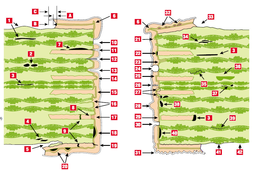
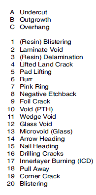
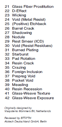 Figure: Typical phenomena in cross-section of PTH. Not all phenomena are specified in ECSS-Q-ST-70-60 in the same way.
ANNEX(informative)Cleanliness requirements for laminate and prepreg
Introduction
The text from this annex is cited from Appendix A from IPC-4101E and was originally drafted by European space industry. The text is provided for information. The full standard and any future revisions can be obtained from IPC.
Citation of Appendix A from IPC-4101E
APPENDIX A from IPC-4101E supplemental inspection requirements if required in purchase order or master drawing.
A.1 - SCOPE
This Appendix A defines supplemental requirements to this standard [IPC-4101E] with the purpose to define a high quality for base materials to be used for high reliability PWBs for critical applications. PWBs designed with small spacing or used in high voltage applications can be subject to failure of insulation resistance due to breakdown or inclusion of foreign material.
Printed boards that meet the requirements of IPC-6012DS ‘‘Space and Military Avionics Applications Addendum, Section 0.1.1 Purpose,’’ are not allowed to have foreign inclusions that reduce dielectric spacing to below the minimum requirement. The requirements on base materials in this appendix aim to prevent and to detect such nonconformance earlier in the supply chain.
If the user of material wishes to acquire laminate, prepreg or both that meet the requirements of this Appendix A, then this Appendix A shall be specifically called out in the purchase order or the master drawing. Further, this Appendix A shall not be assumed to be in force if it is not specifically called out in the purchase order or the master drawing.
A.2 - PREPREG
A.2.1 Acceptance Criteria for Prepreg Requirements 3.8.3.2.1 and 3.8.3.2.2 shall apply for inclusions and imperfections in prepreg.
A.2.2 Test Method for Prepreg Prepreg shall be tested in accordance with Table 3-2 for visual properties, with the following modification:
– Conformance testing of visual properties shall be performed on 100% of the units in a lot using IPC-TM-650, Method 2.1.5, or an equivalent method AABUS. Modify Method 2.1.5 by changing the particulate inspection magnification to 50X.
A.2.3 Rejection Criteria for Prepreg Section 4.4.3 shall be discarded for rejected lots. The following modification shall apply:
– Material with nonconformances shall be discarded from the batch. The remainder of the batch shall be compliant with this Appendix A.
A.3 - LAMINATE
A.3.1 Acceptance Criteria for Laminate The requirements of 3.8.3.1.6 shall apply for imperfections on laminate, with the following modification:
– Requirement ‘f’ shall be deleted and the following shall apply: Opaque foreign matter shall not exceed 0.50 mm [0.019 in]. Opaque foreign inclusions <0.13 mm [0.005 in] shall not be counted. Opaque foreign inclusions sized between 0.13 mm [0.005 in] and ≤0.50 mm [0.019 in] shall average no more than two spots per 300 mm x 300 mm [11.81 in x 11.81 in] area inspected.
A.3.2 Test Method for Laminate Laminate shall be tested in accordance with Table 3-1 for surface and sub-surface imperfections, with the following modification:
– The conformance testing of surface and sub-surface imperfections shall be performed on ≥2% of the total area of the lot.
A.3.3 Rejection Criteria for Laminate Section 4.4.3 shall be discarded for rejected lots. The following modification shall apply:
– All base material in the lot shall be non-compliant to this Appendix A if non-conformances are observed in the lot.
A.3.4 In-Process Requirement for Laminate For the manufacture of copper clad laminate, the base material supplier shall use prepreg that is inspected and evaluated in accordance with A.2 or AABUS.
A.3.5 Hi-Pot Test for Laminate Hi-Pot testing as per IPC-TM-650, Method 2.5.7.2, can be performed AABUS on 100% of the copper clad laminate with a nominal thickness of ≤0.119 mm [0.0047 in]. The preparation of edges of the laminate, the bake out, the electrical test parameters and the acceptance criteria are AABUS.
A.4 - APPLICABILITY
Section 4.2 shall apply for the responsibility of conformance testing performed by the base material manufacturer, with the following modification:
– The procurement authority has the right to perform inspections set forth in this Appendix A to verify acceptability of the lot, in which case the requirements of this Appendix A shall apply.
A.5 - CERTIFICATE OF CONFORMANCE
Section 4.4.5 shall apply for the certificate of conformance, with the following modification:
– The certificate of conformance shall include a statement of compliance to this Appendix A.
A.6 - QUALITY CONFORMANCE INSPECTION AND FREQUENCY
Sections 4.4 and 4.4.1 shall apply for quality conformance inspection and frequency with the following modification:
– The manufacturer’s quality system shall not take precedence over the requirements in Appendix A.
Table A-1 Summary Table of Modifications in Appendix A
|
Tests |
Requirement paragraph IPC-4101E |
Test Method |
Qualification Testing |
Conformance Testing |
Conformance Testing Frequency |
Inspected specimens |
|
Visual properties for prepreg |
3.8.3.2 |
2.1.5 or AABUS |
|
|
Lot |
100% of the lot as per A.2.2 |
|
Surface and Sub-Surface Imperfections for laminate |
3.8.3.1.6 and A.3 |
2.1.5 or AABUS |
|
|
Lot |
≥2% of the lot as per A.3.2 |
|
Hi-Pot electrical test on laminate |
A.3.5 |
2.5.7.2 or AABUS |
AABUS |
AABUS |
- |
100% or AABUS |
ANNEX(informative)Example qualification programme
|
Test vehicle ID as per figure 7-1 |
Group |
Clause or req. in ECSS-Q-ST-70-60 |
Test description (initial test as received) |
Clause or req. in ECSS-Q-ST-70-60 |
Test description (subsequent test after stress) |
Nr ofsamples |
Running item nr |
|
PCB 1-3 |
group 1 |
9.3.2 |
visual inspection for qualitative aspects |
- |
- |
3 |
1 |
|
PCB 1-3 |
group 1 |
9.3.3 |
visual inspection for dimensional verification |
- |
- |
3 |
2 |
|
PCB 1-3 |
group 1 |
9.3.3.2 |
warp |
- |
- |
3 |
3 |
|
PCB 1-3 |
group 1 |
9.3.3.3 |
twist |
- |
- |
3 |
4 |
|
3 coupons |
group 1 |
9.3.4 |
impedance test |
- |
- |
3 |
5 |
|
3 coupons |
group 1 |
9.3.5 |
dielectric constant and loss tangent |
- |
- |
3 |
6 |
|
PCB 1 |
group 1 |
9.3.6 |
cleanliness |
- |
- |
1 |
7 |
|
PCB 1-3 |
group 1 |
9.3.7.2 |
high resistance electrical test |
- |
- |
3 |
8 |
|
PCB 1-3 |
group 1 |
9.3.8 |
continuity test |
- |
- |
3 |
9 |
|
1 coupon |
group 2 |
9.4.2 |
peel test |
- |
- |
1 |
10 |
|
2 coupons |
group 2 |
9.4.3 |
flexural fatigue |
- |
- |
2 |
11 |
|
2 coupons |
group 2 |
" |
" |
9.4.3h |
resistance before and after test |
2 |
12 |
|
2 coupons |
group 2 |
" |
" |
9.3.2, 10.4 |
visual inspection |
2 |
13 |
|
2 coupons |
group 2 |
" |
" |
9.5.2, 10.3 |
microsectioning for qualitative aspects |
2 |
14 |
|
1 coupon or 1 PCB sample |
group 2 |
9.4.4 |
bending test |
- |
- |
1 |
15 |
|
1 coupon or 1 PCB sample |
group 2 |
" |
" |
9.4.3h |
resistance before and after test |
1 |
16 |
|
1 coupon or 1 PCB sample |
group 2 |
" |
" |
9.3.2, 10.4 |
visual inspection |
1 |
17 |
|
2 locations |
group 2 |
" |
" |
9.5.2, 10.3 |
microsectioning for qualitative aspects |
2 |
18 |
|
1 coupon |
group 2 |
9.4.5 |
coating adhesion - tape test |
- |
- |
1 |
19 |
|
1 coupon |
group 2 |
9.4.6 |
analysis of SnPb |
- |
- |
1 |
20 |
|
1 coupon |
group 2 |
9.4.7 |
outgassing |
- |
- |
1 |
21 |
|
1 coupon |
group 2 |
9.4.8b |
TGA: Td |
- |
- |
1 |
22 |
|
1 coupon |
group 2 |
9.4.8d |
DSC: Tg |
- |
- |
1 |
23 |
|
1 coupon |
group 2 |
9.4.8c, 9.4.8e, 9.4.8f |
TMA: T288, Tg, CTE |
- |
- |
1 |
24 |
|
1 coupon |
group 2 |
9.4.11 |
solderability, without microsectioning |
- |
- |
1 |
25 |
|
3 coupons and 1 PCB sample |
group 3 |
9.5.2, 10.2, 10.3 |
microsectioning for qualitative aspects, dimensional verification |
- |
- |
4 |
26 |
|
3 coupons and 1 PCB sample |
group 3 |
9.5.3 |
solder bath float |
- |
- |
4 |
27 |
|
3 coupons and 1 PCB sample |
group 3 |
" |
" |
9.3.2, 10.4 |
visual inspection |
4 |
28 |
|
3 coupons and 1 PCB sample |
group 3 |
" |
" |
9.5.2, 10.3 |
microsectioning for qualitative aspects |
4 |
29 |
|
3 coupons |
group 3 |
9.5.4 |
rework simulation |
- |
- |
3 |
30 |
|
3 coupons |
group 3 |
" |
" |
9.5.2, 10.3 |
microsectioning for qualitative aspects |
3 |
31 |
|
3 coupons |
group 3 |
9.5.5 |
IST test |
- |
- |
3 |
32 |
|
3 coupons |
group 3 |
" |
" |
9.5.2, 10.3 |
microsectioning for qualitative aspects |
3 |
33 |
|
2 PCB samples |
group 4 |
9.6.2c.2 |
intralayer insulation resistance DC as per 9.6.3 |
- |
- |
2 |
34 |
|
2 PCB samples |
group 4 |
" |
interlayer insulation resistance DC as per 9.6.3 |
- |
- |
2 |
35 |
|
2 PCB samples |
group 4 |
9.6.2c.3 |
intralayer dielectric withstanding voltage DC as per 9.6.4 |
- |
- |
2 |
36 |
|
2 PCB samples |
group 4 |
" |
interlayer dielectric withstanding voltage DC as per 9.6.4 |
- |
- |
2 |
37 |
|
2 PCB samples |
group 4 |
9.6.2c.4 |
reflow simulation as per 9.8.3 |
- |
- |
2 |
38 |
|
2 PCB samples |
group 4 |
9.6.2c.5 |
rework simulation on 4 PTH as per 9.5.4 |
- |
- |
2x4 |
39 |
|
2 PCB samples |
group 4 |
9.6.2c.6 |
thermal cycling as per 9.6.2c.6 (500x, from -55 to +100 degC) |
- |
- |
2 |
40 |
|
2 PCB samples |
group 4 |
" |
" |
9.6.2c.7 |
intralayer insulation resistance DC as per 9.6.3 |
2 |
41 |
|
2 PCB samples |
group 4 |
" |
" |
" |
interlayer insulation resistance DC as per 9.6.3 |
2 |
42 |
|
2 PCB samples |
group 4 |
" |
" |
9.6.2c.8 |
intralayer dielectric withstanding voltage DC as per 9.6.4 |
2 |
43 |
|
2 PCB samples |
group 4 |
" |
" |
" |
interlayer dielectric withstanding voltage DC as per 9.6.4 |
2 |
44 |
|
2 PCB samples |
group 4 |
" |
" |
9.6.2c.9 |
peel test |
2 |
45 |
|
10 microsections |
group 4 |
" |
" |
9.6.2c.10, 9.6.2c.11 |
microsectioning for qualitative aspects |
10 |
46 |
|
4 coupons |
group 5 |
9.7.2 |
THB |
- |
- |
4 |
47 |
|
4 coupons |
group 5 |
" |
" |
9.5.2 |
microsectioning |
4 |
48 |
|
10 coupons |
group 5 |
9.7.3 |
CAF |
- |
- |
10 |
49 |
|
10 coupons |
group 5 |
" |
" |
9.5.2 |
microsectioning |
10 |
50 |
|
1 PCB sample |
group 6 |
9.8.2c.2 |
reflow simulation as per 9.8.3 |
- |
- |
1 |
51 |
|
1 PCB sample |
group 6 |
9.8.2c.3 |
rework simulation on 4 PTH as per 9.5.4 |
- |
- |
1x4 |
52 |
|
1 PCB sample |
group 6 |
9.8.2c.4 |
thermal cycling as per 9.8.4 (200x, from -60 to +140 degC) |
- |
- |
1 |
53 |
|
10 microsections |
group 6 |
" |
" |
9.8.2c.5 |
microsectioning for qualitative aspects |
10 |
54 |
Bibliography
|
ECSS-S-ST-00
|
ECSS system – Description, implementation and general requirements
|
|
ECSS-Q-ST-70-07
|
Space product assurance — Verification and approval of automatic machine wave soldering
|
|
ECSS-Q-ST-70-28
|
Space product assurance — Repair and modification of printed circuit board assemblies for space use
|
|
IEC 60068-2-3 (196901)
|
Environmental testing. Part 2: Tests. Test Ca: Damp heat, steady state
|
|
IEC 60068-2-14-am 1 (1986-01)
|
Environmental testing. Part 2: Tests. Test N: Change of temperature
|
|
IEC 60068-2-20-am 2 (1987-01)
|
Environmental testing. Part 2: Tests. Test T: Soldering
|
|
IEC 60249-1-am 4 (1993-05)
|
Base materials for printed circuits. Part 1: Test methods
|
|
IEC 60326-5-am 1 (1989-10)
|
Printed boards. Part 5: Specification for single and double sided printed boards with platedthrough holes
|
|
IEC 60326-8 (1981-01)
|
Printed boards. Part 8: Specification for single and double sided flexible printed boards with through connections
|
|
IEC 60326-11 (1991-03)
|
Printed boards. Part 11: Specification for flexrigid multilayer printed boards with through connections
|
|
IEC 62326-4 (1996-12)
|
Printed boards. Part 4: Rigid multilayer printed boards with interlayer connections Sectional specification
|
|
MIL-P-50884C (1984)
|
Printed wiring, flexible and rigidflex
|
|
IPC-J-STD-003C (2013)
|
Solderability test for printed boards
|
|
IPC-1601A (2016)
|
Printed Board Handling and Storage Guidelines
|
|
IPC-2221B (2012)
|
Generic standard on printed board design
|
|
IPC-5703 (2013)
|
Cleanliness guidelines for printed board fabricators
|
|
IPC-5704 (2009)
|
Cleanliness requirements for unpopulated printed boards
|
|
IPC-6011 (1996)
|
Generic performance specification for printed boards
|
|
IPC-6013DS (to be issued)
|
Space and military avionics applications addendum to IPC-6013D
|
|
IPC-9252B (2016)
|
Requirements for electrical testing of unpopulated printed boards
|
|
IPC-9691B (2016)
|
User Guide for the IPC-TM-650, Method 2.6.25, Conductive Anodic Filament (CAF) Resistance and Other Internal Electrochemical Migration Testing
|