
Space product assurance
High reliability assembly for surface mount and through hole connections
Foreword
This Standard is one of the series of ECSS Standards intended to be applied together for the management, engineering, product assurance and sustainability in space projects and applications. ECSS is a cooperative effort of the European Space Agency, national space agencies and European industry associations for the purpose of developing and maintaining common standards. Requirements in this Standard are defined in terms of what shall be accomplished, rather than in terms of how to organize and perform the necessary work. This allows existing organizational structures and methods to be applied where they are effective, and for the structures and methods to evolve as necessary without rewriting the standards.
This Standard has been prepared by the ECSS-Q-ST-70-61C Working Group, reviewed by the ECSS Executive Secretariat and approved by the ECSS Technical Authority.
Precedence
Line drawings and illustrations are depicted herein to assist in the interpretation of the written requirements of this standard. The text takes precedence over the figures.
Disclaimer
ECSS does not provide any warranty whatsoever, whether expressed, implied, or statutory, including, but not limited to, any warranty of merchantability or fitness for a particular purpose or any warranty that the contents of the item are error-free. In no respect shall ECSS incur any liability for any damages, including, but not limited to, direct, indirect, special, or consequential damages arising out of, resulting from, or in any way connected to the use of this Standard, whether or not based upon warranty, business agreement, tort, or otherwise; whether or not injury was sustained by persons or property or otherwise; and whether or not loss was sustained from, or arose out of, the results of, the item, or any services that may be provided by ECSS.
Published by: ESA Requirements and Standards Section ESTEC, P.O. Box 299, 2200 AG Noordwijk The NetherlandsCopyright: 2022© by the European Space Agency for the members of ECSS## Change log
|
ECSS-Q-ST-70-61C
|
First issue
|
Introduction
This document defines the technical requirements and quality assurance provisions for the manufacture and verification of high-reliability electronic circuits of surface mount, through hole, solderless assemblies, and soldering of harness and wire interconnection, for space applications, launchers, and associated equipment.
In the following table, principal types of through hole components and SMDs, including examples, can be gathered in the following families.
In the text of this document the term “component” is used instead of “device”.
|
THROUGH HOLE COMPONENTS (non exhaustive list) |
|
|
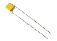
Radial component
|
|
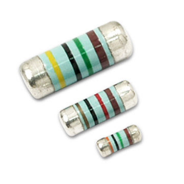
|
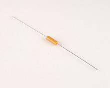
Axial component
|
|
|
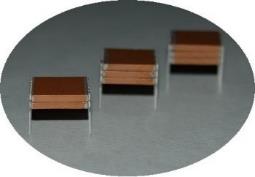
Stacked capacitors
|
|
|
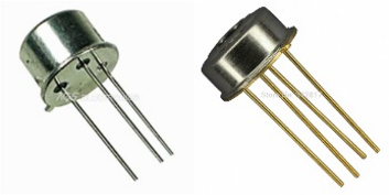
TO Metal Can package
|
|
|
TO Metal tab package
|

|
|
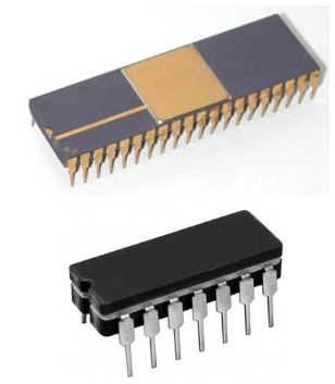
Dual in Line Package (DIL or DIP)
|
|
|
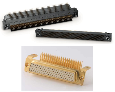
Connectors
|
|
|
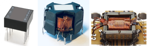
Leaded magnetics
|
|
|
Sculptured flex
|

|
|
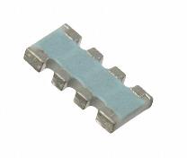
SMT COMPONENTS (non exhaustive list) |
|
|
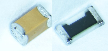
Rectangular and square end-capped or end-metallized component with rectangular body, leadless chip (see 10.4.2)
|
|
|
ceramic end capped chip resistors and capacitors. |
|
|
ceramic resistors arrays |
|
|
metallic terminations
|
|
|
metallic termination resistor
|

|
|
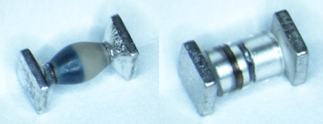
Cylindrical and square end-capped components with cylindrical or oval body, leadless chip (see 10.4.3)
|
|
|
MELF for cylindrical end capped:
|

|
|
Resistors in MELF, minimelf or micromelf
|
|
|
Square end capped:
|
|
|
Bottom terminated chip component (see 10.4.4)
|
|
|
Chip inductors
|
|
|
Component with inward formed L-shaped leads (see 10.4.5)
|
|
|
moulded tantalum chip capacitors. |
|
|
SMD moulded shunt
|
|
|
Leadless component with plane termination (see 10.4.6)
|
|
|
With metal plane termination: SMD0.5, SMD1, SMD2, SMD0.2*(TO276 JEDEC family denomination)
|

|
|
With non-metal plane termination: SMD0.2*
|

|
|
Leaded component with plane termination (see 10.4.7)
|

|
|
Leadless castellated ceramic chip carrier component (see 10.4.8)
|
|
|
The main component of this type is leadless ceramic chip carrier (LCCC) |
|
|
LCC6 |
|
|
No lead QFN (see 10.4.9)
|
|
|
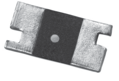
Flat pack and gull-wing leaded component (see 10.4.10)
|
|
|
small-outline transistor (SOT), small-outline package (SO), flat pack and quad flat pack (QFP) and SMD connectors with stress-relief (MHD).
|
|
|
transformers
|
|
|
“J” leaded component
|
|
|
Components with ribbon terminals without stress relief (flat lug leads) (see 10.4.12)
|
|
|
Stacked modules components with leads protruding vertically from bottom (see 10.4.13)
|
|
|
Area array components (AAD) (see 10.4.14)
|
 |
|
Solderless connection (see 10.7)
|
 |
|
solderless interposers for LGA or connectors
|

|
Scope
This Standard defines the technical requirements and quality assurance provisions for the manufacture and verification of high-reliability electronic circuits of surface mount, through hole, solderless assemblies and soldering of harness and wire interconnection.
The Standard defines workmanship requirements, the acceptance and rejection criteria for high-reliability assemblies intended to withstand ground testing conditions including LTS (long term storage) and the environment imposed by space flight and launchers.
The mounting and supporting of components, terminals and conductors specified in this standard applies only to assemblies designed to continuously operate over the mission within the temperature limits of -55 °C to +85 °C at solder joint level.
Requirements related to printed circuit boards are contained in ECSS-Q-ST-70-60 and ECSS-Q-ST-70-12.
This standard does not cover lead-free soldering and associated requirements.
This Standard does not cover the qualification and acceptance of the EQM and FM equipment with high-reliability electronic circuits of surface mount, through hole and solderless assemblies.
This Standard does not cover verification of thermal properties for component assembly.
This Standard does not cover pressfit connectors due to the possible damage in the PCB that is not evaluated within this test requirement.
The qualification and acceptance tests of equipment manufactured in accordance with this Standard are covered by ECSS-E-ST-10-03.
This standard may be tailored for the specific characteristics and constraints of a space project, in accordance with ECSS-S-ST-00.
Normative references
The following normative documents contain provisions which, through reference in this text, constitute provisions of this ECSS Standard. For dated references, subsequent amendments to, or revision of any of these publications do not apply. However, parties to agreements based on this ECSS Standard are encouraged to investigate the possibility of applying the more recent editions of the normative documents indicated below. For undated references, the latest edition of the publication referred to applies.
|
ECSS-S-ST-00-01
|
ECSS system - Glossary of terms
|
|
ECSS-M-ST-40
|
Space project management - Configuration and information management
|
|
ECSS-Q-ST-10-09
|
Space product assurance - Nonconformance control system
|
|
ECSS-Q-ST-20
|
Space product assurance - Quality assurance
|
|
ECSS-Q-ST-60
|
Space product assurance - Electrical, electronic and electromechanical (EEE) components
|
|
ECSS-Q-ST-60-05
|
Space product assurance - Generic requirements for hybrids
|
|
ECSS-Q-ST-60-13
|
Space product assurance - Commercial electrical, electronic and electromechanical (EEE) components
|
|
ECSS-Q-ST-70
|
Space product assurance - Materials, mechanical parts and processes
|
|
ECSS-Q-ST-70-01
|
Space product assurance - Cleanliness and contamination control
|
|
ECSS-Q-ST-70-02
|
Space product assurance - Thermal vacuum outgassing test for the screening of space materials
|
|
ECSS-Q-ST-70-12
|
Space product assurance - Design rules for printed circuit boards
|
|
ECSS-Q-ST-70-28
|
Space product assurance - Repair and modification of printed circuit board assemblies for space use
|
|
ECSS-Q-ST-70-60
|
Space product assurance -Qualification and procurement of printed circuit boards
|
|
ECSS-Q-ST-70-71
|
Space product assurance -Materials processes and their data selection
|
|
ESA-STR-258
|
ESA-Approved Skills Certification Requirements
|
|
ESCC 23500 (September 2013)
|
Requirements for lead materials and finishes for components for space application
|
|
IPC J-STD-001H
|
Requirements for Soldered Electrical and Electronic
|
|
IPC J-STD-004B-AM1 (November 2011)
|
Requirements for Soldering Fluxes
|
|
IPC J -STD-033D (January 2018)
|
Handling, Packing, Shipping and Use of Moisture, Reflow, and Process Sensitive Devices
|
|
IPC-TM-650
|
Test methods manual. Surface Insulation Resistance, Fluxes
|
|
ISO 9454-1:2016
|
Soft soldering fluxes; classification and requirements
|
|
ISO 14644-1:2015
|
Cleanrooms and controlled environments
|
|
MIL-STD-883 K Method 2009 (April 2016)
|
Test Method Standard, Microcircuits
|
Terms, definitions and abbreviated terms
Terms from other standards
For the purpose of this Standard, the terms and definitions from ECSS-S-ST-00-01 apply.
For the purpose of this Standard, the terms and definitions from ECSS-Q-ST-60 apply, in particular for the following term(s):
commercial component
For the purpose of this Standard, the terms and definitions from ECSS-Q-ST-70-28 apply, in particular for the following term(s):
repair
rework
Terms specific to the present standard
Approval Authority
entity that reviews and accepts the verification programme, evaluating the test results and grants the final approval
assembly sensitive component
component prone to have cracks in solder joint exceeding 75 % of acceptance criteria of solder cracks or showing nonconformance outside the component manufacturer limit, due to assembly.
- 1 The ESA list of assembly sensitive components is regularly updated and published on ESCIES for information, see www.escies.org, Technologies - ESA SMT Verification. ESA-TECMSP-MO-018961.
- 2 Each company maintains its own list of assembly sensitive components in the PID.
bifurcated terminal
terminal containing a slot or split in which wires or leads are placed before soldering
The term "split terminal" is synonymous.
blister
delamination in form of localized swelling and separation between any of the layers of a laminated base material in a printed circuit board
bonding
application process of adhesive underneath a package for mechanical or thermal purpose
bridging
build-up of solder or conformal coating between components, component leads or base substrate forming an elevated path
clinched lead
conductor or component lead which passes through a printed circuit board and is then bent to contact the printed circuit board pad
The clinched portion is not forced to lie flat on the pad and some innate spring back is desirable before this form of termination is soldered.
cold flow
tendency of a solid material to move slowly or deform permanently under the influence of persistent mechanical stresses.
For example, for PTFE (Teflon) insulation sleeves under pressure.
cold solder joint
joint in which the solder has a blocky, wrinkled or piled-up appearance and shows signs of improper flow or wetting action
It can appear either shiny or dull, but not granular. The joint normally has abrupt lines of demarcation rather than a smooth, continuing fillet between the solder and the surfaces being joined. These lines are caused by either insufficient application of heat or the failure of an area of the surfaces being joined to reach soldering temperature.
conformal coating
thin polymeric film applied on a populated PCB that conforms to the shape of the surface it covers.
co-planarity
difference between maximum and minimum termination height when component rests on flat surface
collective assembled components
set of components that are soldered to PCB in one operation
For example, vapour phase soldered components, in contrast to manually soldered where each component is soldered individually.
critical zone
area in the solder joint in which the existence and magnitude of cracks is subject to acceptance or rejection
dewetting
condition in a soldered area in which the liquid solder has not adhered intimately, characterized by an abrupt boundary between solder and conductor, or solder and terminal/termination area
This is often seen as a dull surface with islands of thicker shiny solder.
disturbed solder joint
unsatisfactory connection resulting from relative motion between the conductor and termination during solidification of the solder
dynamic wave soldering machine
system that achieves wave soldering and which consists of stations for fluxing, preheating, and soldering by means of a conveyor
electrical clearance
spacing between separate electrical conductors of a printed circuit board assembly
exposed pad
exposed metallization on the bottom of a package
The exposed pad can have both electrical or thermal purpose and is often plated with same material and finish as the edge terminations, for soldering purposes. Exposed pad can be thermally bonded, soldered or left unconnected if not needed for the intended application.
fillet
smooth concave build-up of material between two surfaces
Example: A fillet of solder between a component lead and a solder pad or terminal, or a fillet of conformal coating material between a component and printed circuit board.
flux
material which, during soldering, removes the oxide film, protects the surface from oxidation, and permits the solder to wet the surfaces to be joined
glass meniscus
glass fillet of a lead seal which occurs where an external lead leaves the package body
modal survey
characterization of the dynamic properties of systems in the frequency domain
A typical example is testing structures under vibrational excitation
outsourcing
act of subcontracting work to another company in compliance with customer PID
pin in paste
process where a through hole component is mounted and soldered in the surface mounting process
pits
small holes or sharp depressions in the surface of solder
This can be caused by flux blow-out due to entrapment or overheating.
potting compound
compound, usually electrically non-conductive, used to encapsulate or as a filler between components, conductors, or assemblies
pressfit connector
solderless termination technology where each contact is pressed into a plated hole of a printed circuit board creating a mechanical and electrical joint
reprocessing
preparatory operation done on a component prior to assembly
Degolding, pretinning, lead forming, and cutting are examples of reprocessing.
shield
metallic sheath surrounding one or more wires, cables, cable assemblies, or a combination of wires and cables that is used to prevent or reduce the transmission of electromagnetic energy to or from the enclosed conductors
The shield also includes an insulating jacket that can cover the metallic sheath.
solder balls
numerous spheres of solder having not melted in with the joint form and being scattered around the joint area normally attached by flux residues
Can be caused by incorrect preheating or poor-quality solder.
solder-cup terminal
hollow, cylindrical terminal closed at one end to accommodate one or more conductors
solder icicle
conical peak or sharp point of solder usually formed by the premature cooling and solidification of solder upon removal of the heat sources
solder pad
conductive surface on a printed circuit board to which terminations are soldered to form electrical connections
solder stand-off
thickness of solder between the underside of the component termination and the solder pad
split terminal
see "bifurcated terminal" 3.2.3
staking
application process of adhesive on the outside of a package for mechanical purpose
stress relief
method or means to minimize stresses to the soldered termination or component
Generally, in the form of a bend or service loop in a component lead, solid or stranded wire to provide relief from stress between terminations, as that caused, for instance by movement or thermal expansion.
stud termination
upright conductor termination through a printed circuit board
technology samples
samples of boards assembled with representative technology
thermal shunt
element with good heat-dissipation characteristics used to conduct heat away from an article being soldered
turret terminal
round post-type grooved stud around which conductors are fastened before soldering
underfill
material deposited between a component and substrate
verification board
substrate assembled with components subjected to a verification programme
wicking
flow of molten solder or cleaning solution by capillary action
Occurs when joining stranded wire; solder is drawn within the strands, but normally not visible on outer surface of strands. Wicking can also occur within the stress relief bend of a component lead.
Abbreviated terms
For the purpose of this Standard, the abbreviated terms from ECSS-S-ST-00-01 and the following apply:
|
Abbreviation
|
Meaning
| |
|
AAD
|
area array device
| |
|
AOI
|
automatic optical inspection
| |
|
AWG
|
American wire gauge
| |
|
AXI
|
automatic X-ray inspection
| |
|
BGA
|
ball grid array
| |
|
CBGA
|
ceramic ball grid array
| |
|
CCGA
|
ceramic column grid array
| |
|
CGA
|
column grid array
| |
|
CLCC
|
ceramic leadless chip carrier
| |
|
CTE
|
coefficient of thermal expansion
| |
|
DCL
|
declared component list
| |
|
DIL
|
dual in line
| |
|
DIP
|
dual in line package
| |
|
DPAK
|
diode package
| |
|
DRD
|
document requirement definition
| |
|
EDX
|
Energy dispersive X-ray
| |
|
ETFE
|
ethylene tetrafluoroethylene
| |
|
EPA
|
ESD protected area
| |
|
ESD
|
electrostatic discharge
| |
|
FEP
|
fluorinated ethylene propylene
| |
|
FM
|
flight model or flight hardware
| |
|
FP
|
flat pack package
| |
|
IST
|
interconnect stress testing
| |
|
JEDEC
|
Joint Electron Component Engineering Council
| |
|
LCCC
|
leadless ceramic chip carrier
| |
|
MELF
|
metal electrode face bonded
| |
|
MIP
|
mandatory inspection point
| |
|
MPCB
|
Materials, Mechanical Parts and Processes Control Board
| |
|
MRR
|
manufacturing readiness review
| |
|
MSL
|
moisture sensitivity level
| |
|
PCB
|
printed circuit board
| |
|
PLCC
|
plastic leaded chip carrier
| |
|
PID
|
process identification document
| |
|
PSD
|
power spectral density
| |
|
PTFE
|
polytetrafluoroethylene
| |
|
PTH
|
plated though hole
| |
|
QFN
|
quad flat pack no leads
| |
|
QFP
|
quad flat pack
| |
|
Rg
|
resistance to ground
| |
|
Rs
|
surface resistance
| |
|
r.m.s.
|
root-mean-square
| |
|
SEM
|
scanning electronic microscope
| |
|
SIR
|
surface insulation resistance
| |
|
SMD
|
surface mounted device
| |
|
SMT
|
surface-mount technology
| |
|
SO
|
small outline
| |
|
SOD
|
small outline diode
| |
|
SOT
|
small outline transistor
| |
|
SOP
|
small outline package
| |
|
TO
|
transistor outline
| |
|
TRB
|
test review board
| |
|
TRR
|
test readiness review
| |
|
TSOP
|
thin small outline package
| |
|
RF
|
radio frequency
| |
Nomenclature
The following nomenclature apply throughout this document:The word “shall” is used in this document to express requirements. All the requirements are expressed with the word “shall”.
The word “should” is used in this document to express recommendations. All the recommendations are expressed with the word “should”.
It is expected that, during tailoring, all the recommendations in this standard are either converted into requirements or tailored out.
The words “may” and “need not” are used in this document to express positive and negative permissions respectively. All the positive permissions are expressed with the word “may”. All the negative permissions are expressed with the words �“need not”.
The word “can” is used in this document to express capabilities or possibilities, and therefore, if not accompanied by one of the previous words, it implies descriptive text.
In ECSS “may” and “can” have a completely different meaning: “may” is normative (permission) and “can” is descriptive.
The present and past tense are used in this document to express statement of fact, and therefore they imply descriptive text.
Principles of reliable soldered connections
The following are the general principles to provide reliable soldered connections:
Reliable soldered connections are the result of proper design, control of tools, materials, processes work environments and workmanship performed in accordance to verified and approved procedures, inspection control and precautions.
The basic design concepts to provide reliable connections and to avoid solder joint failure are as follows:
Stress relief is an inherent part of the design which reduces detrimental thermal and mechanical stresses on the solder connections.
Where adequate stress relief is not possible materials are so selected that the mismatch of thermal expansion coefficients is a minimum at the constraint points in the component mounting configuration.
The assembled substrates are designed to allow easy inspection, rework, and repair.
The electrical and mechanical integrity of components and assemblies are retained after exposure to processes employed during manufacture and assembly, as handling, baking, fluxing, soldering, cleaning depanelization, electrical test and PCB integration.
Soldering to gold using tin-lead alloy can cause failure.
Preparatory conditions
Facility cleanliness
ECSS-Q-ST-70-61_1510001Personnel facilities shall be separated from the soldering areas.
Example: Washrooms, eating areas, smoking facilities.
ECSS-Q-ST-70-61_1510002Furniture shall be arranged to allow thorough cleaning of the floor and workbench.
ECSS-Q-ST-70-61_1510003Areas used for soldering shall be kept free from contaminants.
Loose material such as dirt, dust, solder particles, oil or clipped wires can contaminate soldered connections.
ECSS-Q-ST-70-61_1510004Working areas shall be kept free from any tools or equipment not used for the current task.
ECSS-Q-ST-70-61_1510005Working surfaces shall be covered with an easily cleaned hard top or have a replaceable surface of clean, non-corrosive, silicone-free ESD compatible paper.
ECSS-Q-ST-70-61_1510006Tools used during soldering operations shall be free of visible contaminant.
ECSS-Q-ST-70-61_1510007Excess lubricants shall be removed from tools before soldering starts.
Environmental conditions
ECSS-Q-ST-70-61_1510008The clean room shall be compliant to the requirements of clause 5.3.1 of ECSS-Q-ST-70-01.
ECSS-Q-ST-70-61_1510009The soldering area shall have as minimum a cleanliness level of ISO Class 8.2 in accordance with ISO 14644-1 (2015).
Particle concentrations for ISO Class 8.2 are not mentioned in the ISO Standard and can only be calculated with the formula in Annex E of ISO 14644-1 (2015). See Table 5-1.
Table 5-1: Particle concentrations classes 8 till 9 according to ISO 14644-1 (2015)
|
Particle sizes
| ||||
|
ISO class
|
0,5 µm
|
1 µm
|
5 µm
|
Comment
|
|
ISO-class 8
|
3 520 000 |
832 000 |
29 300 |
From Table 1 of ISO
|
|
ISO-class 8.1
|
4 430 000 |
1 050 000 |
36 800 |
Calculation acc ISO Annex E equation
|
|
ISO-class 8.2
|
5 570 000 |
1 320 000 |
46 400 |
Calculation acc ISO Annex E equation
|
|
ISO-class 8.5
|
11 100 000 |
2 630 000 |
92 500 |
From Annex E in ISO
|
|
ISO-class 9
|
35 200 000 |
8 320 000 |
293 000 |
From Table 1 of ISO
|
ECSS-Q-ST-70-61_1510010Areas used for assembly or cleaning of components and areas where toxic or volatile vapours are generated or released shall include a local air extraction system.
ECSS-Q-ST-70-61_1510011The room temperature of the facility shall be maintained at (22 ±3) C.
ECSS-Q-ST-70-61_1510012The relative humidity at room temperature of the facility shall be maintained at (55 ±10) %.
ECSS-Q-ST-70-61_1510013The soldering area shall not be exposed to draughts.
ECSS-Q-ST-70-61_1510014Air shall be supplied to the room through a filtering system that provides a positive pressure difference with respect to adjacent rooms.
Lighting requirements
ECSS-Q-ST-70-61_1510015Lighting intensity shall be a minimum of 1080 lux on the work surface.
In selecting a light source, the colour temperature of the light is an important consideration. Light ranges from 3000 K-5000 K enable users to distinguish various printed circuit assembly features and contaminants with increased clarity.
ECSS-Q-ST-70-61_1510016At least 90 % of the work area shall be without shadows or severe reflections.
Precautions against static discharges
Overview
Electronic components are particularly sensitive to electrostatic charging and discharging. To protect these components, it is necessary to define measures with regard to their handling, transport and storage.
The ESD control programme helps reducing to a minimum level the ESD-related damage to components. Main topics of the programme are:
ESD coordinator,
Training,
Product qualification,
Compliance verification,
Grounding/bonding systems,
Personnel grounding,
EPA requirements,
Packaging systems,
Marking.
The controls referenced in this document have been selected from document “ANSI/ESD S20.20-2014 2.0 SCOPE”. The goal is to prevent damage of the isolated conductors and of the ESD sensitive devices (ESDS) which are susceptible to discharges that are greater than or equal to 100 V (Human Body Model) or 200 V (Charged Device Model).
General
ECSS-Q-ST-70-61_1510017An ESD Control Programme in accordance with EN 61340-5-1 (2016) shall be developed and implemented by the supplier.
EN 61340-5-2 guideline can be used for editing the ESD Control Programme.
ECSS-Q-ST-70-61_1510018The process for the selection of new components shall include their ESD sensitivity.
ECSS-Q-ST-70-61_1510019Electrostatic sensitive components shall be handled, prepared, mounted, soldered, and cleaned in an ESD protected area compatible with ESD class of the components.
Electrostatic sensitive components are classified in different categories. For some, additional ESD conditions to the nominal are needed.
ESD Protected Area
ECSS-Q-ST-70-61_1510020ESD sensitive devices shall be assembled in an EPA.
ECSS-Q-ST-70-61_1510021As a minimum, a dissipative mat, a wrist strap and common grounding facility for both shall be in place in the EPA.
ECSS-Q-ST-70-61_1510022EPA areas shall be visibly marked as such.
ECSS-Q-ST-70-61_1510023ESD rules and regulations shall apply as specified in EN 61340-5-1 (2016).
ECSS-Q-ST-70-61_1510024If the measured electrostatic field or surface potential exceeds the stated limits, ionization or other charge mitigating techniques shall be used.
ECSS-Q-ST-70-61_1510025Relative Humidity shall be controlled in the EPA in accordance with requirement 5.2e.
Precautions against ESD during manufacturing
ECSS-Q-ST-70-61_1510026Delimited EPA and corresponding ESD control items shall be in compliance with Table 5-2.
ECSS-Q-ST-70-61_1510027Ionized air in presence of high voltage or RF shall be used in compliance with components manufacturer recommendations.
Static charges on isolated components or tooling can be dissipated using ionised air.
ECSS-Q-ST-70-61_1510028A wrist strap shall be worn by the operator.
ECSS-Q-ST-70-61_1510029Powered equipment at the workstation shall be grounded.
ECSS-Q-ST-70-61_1510030The normal value of the resistance between the tip of the soldering system and the ground of the ESD protected area shall not exceed 5 Ω.
The measurement is generally performed at soldering temperature.
ECSS-Q-ST-70-61_1510031A ground-fault circuit interrupter shall be installed.
ECSS-Q-ST-70-61_1510032Protective clothing shall be made from static dissipative material.
ECSS-Q-ST-70-61_1510033Gloves and finger cots shall be made from static dissipative material.
ECSS-Q-ST-70-61_1510034Tools, such as mounting aids, consumables, masking tape, shall be conductive or static dissipative.
ECSS-Q-ST-70-61_1510035Paperwork accompanying ESD sensitive components shall be contained in static dissipative bags or envelopes.
Example of accompanying paperwork are traveller logs, drawings, and instructions.
ECSS-Q-ST-70-61_1510036Paperwork shall not come into contact with ESD sensitive components.
ECSS-Q-ST-70-61_1510037Table 5-2: EPA requirements summary
|
ESD Control item
|
Limits values *
| |
|
Working surfaces, storage, racks and trolleys
|
Dissipative top surface
|
Rs <1 109
|
|
ESD protected to ground
|
Rg < 1109
| |
|
Flooring
|
ESD protected to ground
|
Rg < 1109
|
|
Ionization
|
|
Decay (1000 V to 100 V) in less than 20 s
|
|
Seating
|
ESD protected to ground
|
Rg <1109
|
|
Wrist strap system
|
ESD protected to ground
|
Rg <35 106
|
|
* Values are taken from Tables 2 and 3 of EN 61340-5-1:2016.
| ||
Protective packaging and ESD protection
ECSS-Q-ST-70-61_1510038All ESD-sensitive items shall be contained within ESD-protective containers for movement between and within ESD-protected areas.
ECSS-Q-ST-70-61_1510039ESD protective packaging shall display ESD warning signs.
ECSS-Q-ST-70-61_1510040If the packaging is not ESD safe, it shall be labelled accordingly.
The objective of ESD protection is to prevent ESD to the item contained within, to allow for dissipation of charge, and to prevent charging of the ESD item by an external electrostatic field.
ECSS-Q-ST-70-61_1510041A container providing mechanical and ESD protection shall be used, whenever the ESD-sensitive electronic assembly is transported within a manufacturing plant or during shipment to external destinations.
This can be achieved by a container with:
- an outer shell that provides adequate mechanical protection for the contents,
- foam or bubble wrap shock absorbing liners that have static shielding covers,
- shielding package for the ESD sensitive contents.
ECSS-Q-ST-70-61_1510042All static-shielding bags shall be metallized.
ECSS-Q-ST-70-61_1510043Bags, film, bubble wrap or foam of Pink-Polyethylene shall not be used near any ESD-sensitive item or within an ESD protected area.
Pink-polyethylene provides little protection against ESD events and voltage fields and is a contaminants source.
ECSS-Q-ST-70-61_1510044Shipping popcorn, foam liners and polystyrene foam shall not be used near ESD-sensitive items unless shielding overwrap protects them.
ECSS-Q-ST-70-61_1510045Electrostatic sensitive components shall be kept in appropriate ESD protected packaging.
For example, kept in shielded bags.
ECSS-Q-ST-70-61_1510046Containers for ESD sensitive components shall be labelled as such.
Equipment and tools
General
ECSS-Q-ST-70-61_1510047Equipment and tools shall be inspected to meet requirements from respective clauses 5.5.2 to 5.5.19.
ECSS-Q-ST-70-61_1510048All tools and inspection equipment shall be maintained and calibrated, and their results recorded in accordance with clause 17.
ECSS-Q-ST-70-61_1510049Equipment shall not generate, induce, or transmit electrostatic charges to components being placed.
ECSS-Q-ST-70-61_1510050Any machine or part of machine, in particular the conveyor, shall be grounded to avoid electrostatic discharge.
ECSS-Q-ST-70-61_1510051Machines and equipment used to solder surface mount components shall either be a type incorporating dynamic single or dual solder wave or be of the solder reflow type.
ECSS-Q-ST-70-61_1510052The supplier shall verify, based on the available documentation, that the equipment do not impose any processing parameters that are in contradiction to the processing parameters given by the individual component data sheets.
Examples of processing parameters include maximum temperature to avoid internal melting, thermal shocks, thermal damages, removal of marking ink, degradation of encapsulating plastic.
ECSS-Q-ST-70-61_1510053Temperature and time profiles for assembly shall be identified by the supplier and approved by the Approval Authority.
ECSS-Q-ST-70-61_1510054The supplier shall identify changes and implement a verification programme in compliance with the requirements from clause 13.
ECSS-Q-ST-70-61_1510055The supplier shall demonstrate the reproducibility of their processes.
Brushes
ECSS-Q-ST-70-61_1510056Medium-stiff natural- or synthetic bristle, ESD-safe, brushes shall be used for cleaning.
- 1 Special care has to be taken not to damage any surface or adjacent materials.
- 2 Brushes with wooden handle can be used.
ECSS-Q-ST-70-61_1510057Brushes shall be cleaned in a solvent in accordance with clause 6.4.
ECSS-Q-ST-70-61_1510058Brushes shall not be damaged by the solvents used for PCB cleaning.
ECSS-Q-ST-70-61_1510059Wire brushes shall not be used.
Cutters and pliers
ECSS-Q-ST-70-61_1510060Cutting edge profiles and cutter usage shall be in accordance with Figure 5-1.
ECSS-Q-ST-70-61_1510061The cutter used for trimming conductor wire and component leads shall shear sharply, producing a clean, flat, smooth-cut surface along the entire cutting edge.
- 1 These measures minimize the transmission of mechanical and shock loads to delicate components.
- 2 Smooth, long-nose pliers or tweezers can be used for attaching or removing conductor wires and component leads.
ECSS-Q-ST-70-61_1510062No twisting action shall occur during the cutting operation.
ECSS-Q-ST-70-61_1510063Cutting edges shall be checked for damage and maintained in a sharp condition.
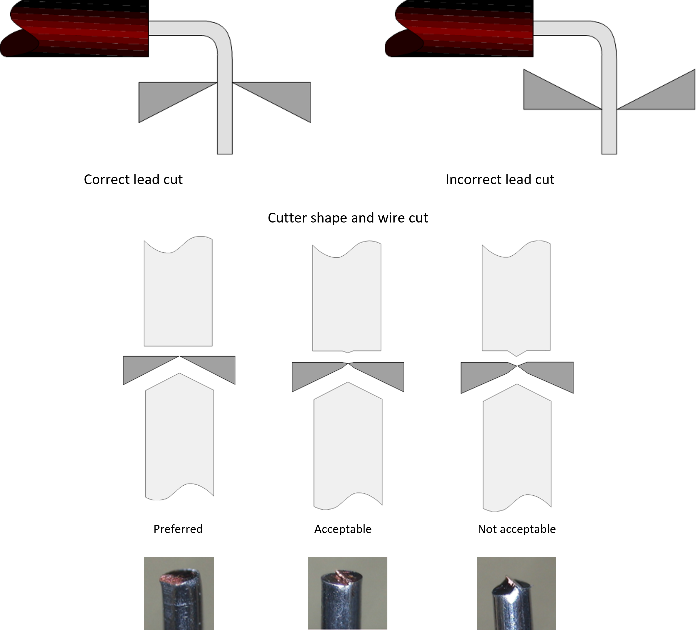 ECSS-Q-ST-70-61_1510064Figure 5-1: Profile of correct cutters for trimming leads
Bending tools
ECSS-Q-ST-70-61_1510065Component leads shall be bent or shaped using tools, including automatic bending tools, which do not nick or damage the leads or insulation.
ECSS-Q-ST-70-61_1510066Components shall not be damaged by the bending process specified in clause 8.2.7.
It is good practice to use bending tools with polished finish.
ECSS-Q-ST-70-61_1510067Bending tools shall have no sharp edges in contact with the component leads.
ECSS-Q-ST-70-61_1510068A maximum reduction of 10 % of initial section of the lead may be acceptable provided that it is representative of the verified configuration.
Clinching tools
ECSS-Q-ST-70-61_1510069Clinching tools shall not damage the surfaces of printed-circuit conductors, components or component leads.
Insulation strippers
Thermal strippers
ECSS-Q-ST-70-61_1510070The temperature of the stripper shall not burn, blister, or cause excessive melting of the insulation.
- 1 Thermal insulation strippers can be used for wire insulation types susceptible to damage by mechanical strippers.
- 2 It is good practice to apply thermal strippers for use with AWG 22 and smaller wire sizes where there is a possibility of the wire stretching if a mechanical stripper is used.
- 3 Local air extraction units can be used during thermal stripping.
Precision mechanical cutting-type strippers
ECSS-Q-ST-70-61_1510071Mechanical strippers shall be of the following types:
- Automatic power-driven strippers with precision, factory-set, cutting, and stripping dies and wire guards, or
- Precision-type hand strippers with accurately machined and factory-pre-set cutting heads.
Figure 5-2 shows an example of acceptable mechanical strippers.
ECSS-Q-ST-70-61_1510072Stripping tools or machines shall fit the size of the wire conductor.
It is good practice to mask off the die openings for wire sizes not in use.
ECSS-Q-ST-70-61_1510073The conductor shall not be twisted, ringed, nicked, cut, or scratched by the process.
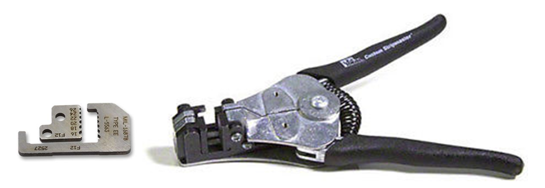 Figure 5-2: Example of suitable mechanical strippers
Enamel stripping for wires
ECSS-Q-ST-70-61_1510074The enamel shall be removed by chemical or thermal means.
ECSS-Q-ST-70-61_1510075The enamel may be removed by mechanical means provided that visual inspection using a minimum magnification of x40 is carried out to confirm absence of damage of the conductor.
ECSS-Q-ST-70-61_1510076When stripping the ends of enamel wires the complete removal of the enamel shall be verified by visual inspection.
ECSS-Q-ST-70-61_1510077Chemical stripping materials shall be completely neutralised and be cleaned such that there are no residues from the stripping, neutralizing, or cleaning steps.
ECSS-Q-ST-70-61_1510078The enamel shall not be visually contaminated by the stripping process.
Verification of stripping tools
ECSS-Q-ST-70-61_1510079Thermal and mechanical stripping tools shall be verified by removal of insulation at the start of each production batch.
Hot air blower
ECSS-Q-ST-70-61_1510080Hot air blower shall be used for shrinking of sleeves
ECSS-Q-ST-70-61_1510081Hot air blower may be used for removal of some adhesives
ECSS-Q-ST-70-61_1510082Hot air blower shall be able to maintain and control a defined temperature.
ECSS-Q-ST-70-61_1510083Temperature of the hot air blower shall be set at a temperature in compliance with the materials and not degrade surrounding assembly or materials.
it is good practice to have a thermocouple around to ensure absence of degradation.
ECSS-Q-ST-70-61_1510084Hot air blower shall meet requirement 5.5.1d against ESD.
Soldering tools
General
ECSS-Q-ST-70-61_1510085The leads shall not be damaged during preparation and assembly.
Holding tools
ECSS-Q-ST-70-61_1510086Holding tools used as soldering aids shall not be wetted by the solder during the assembly.
Thermal shunts
ECSS-Q-ST-70-61_1510087A thermal shunt shall be able to act as heat sink to protect thermally sensitive components.
- 1 An effective clamp-type thermal shunt can be constructed by inserting small copper bars into the jaws of an alligator clip.
- 2 Shunts can be held in place by friction, spring tension or any other means that does not damage the finish or insulation.
Anti-wicking tools
ECSS-Q-ST-70-61_1510088The conductor gauge sizes of the anti-wicking tools shall be marked on the tool.
Anti-wicking tools can be used for pretinning the stranded wires.
Soldering irons
ECSS-Q-ST-70-61_1510089The size and shape of the soldering iron and tip shall not damage adjacent areas or connections during soldering operations.
ECSS-Q-ST-70-61_1510090Temperature-controlled soldering irons shall be used.
ECSS-Q-ST-70-61_1510091Temperature of the solder tip shall be verified once a week and after each solder tip change.
ECSS-Q-ST-70-61_1510092Selected temperature of the solder tip shall remain within +/-10°C.
ECSS-Q-ST-70-61_1510093Resistance between the soldering tip and the workstation grounding point shall be compliant with IPC- J/STD/001H Sept 2020.
ECSS-Q-ST-70-61_1510094AC and DC current leakage from heated tip to ground shall not create deleterious effects on equipment or components.
ECSS-Q-ST-70-61_1510095Tip transient voltages generated by the soldering equipment shall not exceed 2 V peak under a minimum loading impedance of 100 kΩ.
ECSS-Q-ST-70-61_1510096A soldering iron holder shall be used.
It is good practice to use a cage-type holder that leaves the soldering-iron tip unsupported when a temperature-controlled soldering iron is used.
Baking and curing ovens
ECSS-Q-ST-70-61_1510097An oven for baking and curing shall be able to heat and maintain the temperature of a printed circuit board or assembly within ±10 °C.
- 1 It is good practice to take into account the size and number of objects to be heated, when selecting capacity and size of the oven.
- 2 A vacuum oven can be used for drying operation.
ECSS-Q-ST-70-61_1510098An oven used for silicone shall not be used to bake out PCBs.
ECSS-Q-ST-70-61_1510099An oven used for silicone shall not be used to cure adhesives other than silicone.
ECSS-Q-ST-70-61_1510100The oven shall be equipped with an independent automatic shutdown system to protect from overheating.
Solder deposition equipment
ECSS-Q-ST-70-61_1510101Equipment used to deposit solder pastes shall be of a screening, stencilling, dispensing, roller coating, dotting or jet printing type.
ECSS-Q-ST-70-61_1510102Solder deposit equipment shall deposit reproducible amount of solder paste.
The use of Solder Paste Inspection (SPI) equipment helps to ensure reproducible volume of deposited solder paste.
ECSS-Q-ST-70-61_1510103Equipment shall apply pastes of a viscosity and quantity such that the positioned component is retained on the board before and during soldering operations, ensuring self-centring and solder fillet formation.
ECSS-Q-ST-70-61_1510104Equipment used to apply solder preforms shall align the preform with the land or component lead and termination.
ECSS-Q-ST-70-61_1510105Solder paste deposition procedures and associated acceptance criteria shall be controlled and documented.
Automatic component placement equipment
ECSS-Q-ST-70-61_1510106Automatic or computer-controlled equipment used for component placement shall be of the coordinate-driven pick-and-place type or of the robotic type.
ECSS-Q-ST-70-61_1510107The placement equipment used shall be of a type that:
- prevents component or board damages,
- indexes components with respect to the circuit and
- aligns the component terminations with the board terminal areas.
Dynamic wave-solder machines
ECSS-Q-ST-70-61_1510108Dynamic soldering machines shall be of automatic type and of a design offering the following:
- Controlling the flux application.
- Controlling preheating to drive off volatile solvents and to avoid thermal shock damage to the PCB and component packages.
- Maintaining the solder temperature at the printed circuit board assembly to within ±5C of the established bath temperature throughout the duration of any continuous soldering run when measured 3,0 mm below the surface of the wave.
- Having a wave system that limits shadowing and allows solder fillet formation.
- Having carriers made from a material that cannot contaminate, degrade or damage the printed circuit board or substrate nor transmit vibration or shock stress from the conveyors to a degree permitting physical, functional or electrostatic damage to components, board or substrate during transport through preheating, soldering and cooling stages.
- Showing an extraction system, either integral or separate, conforming to the requirements of clause 5.2.
to item 4: It is good practice to use nitrogen atmosphere.
ECSS-Q-ST-70-61_1510109The following wave soldering machine parameters shall be controlled:
- the amount of flux and its coverage,
- the preheat temperature and duration to avoid damage to the PCB and to the component packages,
- the solder temperature so that the solder in the wave making contact with the board is 235 °C to 275 °C. ECSS-Q-ST-70-61_1510110The supplier shall provide evidence that:
- the conveyor speed does not vary by more than ±5 %, and
- the height of the solder wave remains to a constant preselected value across the width of the wave.
Selective wave solder equipment
ECSS-Q-ST-70-61_1510111Selective wave soldering machines shall be of automatic type and of a design offering the following:
- A holding mechanism for the board to be soldered, which can fixate the board during the process, without degrading or damaging the PCB or the mounted components.
- Nozzle, through which a local solder wave applies solder selectively per component or termination, from the solder side of the PCB to the component leads to be soldered.
- Automatic relative movement between nozzle and PCB both in-plane and out-of-plane direction.
- Controllable flux application.
- Maintain the preheating temperature to within 5 C during soldering to avoid thermal shock damage to the PCB and to component packages.
- Maintaining the wave solder temperature to within 5 °C of the established soldering temperature throughout the process.
- Showing an extraction system, either integral or separate, conforming to the requirements of clause 5.2.
to item 2: It is good practice to use local flow of nitrogen around the solder nozzle.
ECSS-Q-ST-70-61_1510112The following selective wave soldering machine parameters shall be controlled:
- the amount of flux and its coverage,
- the preheat temperature,
- the solder temperature so that the solder in the selective wave making contact with the board is maximum 300 °C,
- the nozzle speed so that the soldering time per lead does not exceed 10 s.
Reflow process equipment
Condensation (vapour phase) reflow machines
ECSS-Q-ST-70-61_1510113Condensation reflow machines shall:
- not transmit a movement or vibration into the assemblies being soldered that result in misalignment of components or disturbed solder joints,
- be capable of preheating an assembly with solder paste to the temperature recommended by the solder paste manufacturer prior to soldering,
- use a reflow fluid whose boiling point is a minimum of 17 C above the melting point of the solder being used,
- maintain the preselected temperature to within 5 C in the reflow zone during soldering,
- include an extraction system that conforms to clause 5.2.
to item 3: For boards with high thermal mass or for mixed terminations finish on components, it is a good practice to select a higher peak temperature and to use a delta of 30°C for a good wettability.
ECSS-Q-ST-70-61_1510114Reflow process parameters for condensation reflow machines shall be controlled and documented according to clause 5.5.14.5.
Local hot gas reflow machines
ECSS-Q-ST-70-61_1510115Local hot gas reflow machines shall:
- not transmit movement or vibration to the assemblies being soldered which result in misalignment of components or disturbed solder joints,
- preheat an assembly with solder paste to the temperature recommended by the solder paste manufacturer prior to soldering,
- heat the area of the assembly to be soldered using focused or unfocussed energy, to a preselected temperature that is a minimum of 30C above the melting point of the solder being used as measured at laminate or substrate surface,
- prevent the reflow of adjacent components and components localized on the opposite side,
- prevent excessive temperature that can degrade surrounding materials such as adhesive, underfill,
- Not to be above maximum allowed component temperature,
- maintain the preselected reflow temperature within 5C as measured at the substrate surface. ECSS-Q-ST-70-61_1510116Reflow process parameters for local hot gas reflow machines shall be controlled and documented according to clause 5.5.14.5.
Forced convection and infrared reflow systems
ECSS-Q-ST-70-61_1510117Forced convection and infrared reflow machines shall be of design such that the system:
- provides a controlled temperature profile and does not transmit movement or vibration into the assembly being soldered,
- preheats an assembly with solder paste to the temperature recommended by the solder paste manufacturer prior to soldering,
- heats the area of the assembly to be soldered using focused or unfocussed energy, to a preselected temperature that is a minimum of 30C above the melting point of the solder being used as measured at laminate or substrate surface,
- maintains the preselected temperature to within ±5 C in the reflow zone during soldering,
- not transmit movement or vibration to the assemblies being soldered which result in misalignment of components or disturbed solder joints. ECSS-Q-ST-70-61_1510118Reflow process parameters for forced convection and infrared reflow systems shall be controlled and documented according to clause 5.5.14.5.
Other equipment for reflow soldering
ECSS-Q-ST-70-61_1510119Other solder reflow systems may be approved for use by the Approval Authority under the condition that they meet the requirements of either clause 5.5.14.1, 5.5.14.2 or 5.5.14.3.
Reflow process control parameters
ECSS-Q-ST-70-61_1510120The following reflow process parameters shall be controlled and documented:
- preheat temperature to avoid damage to the PCB, to the component packages and to reduce the solder dwell time,
- solder reflow parameters and cooling parameters to stay inside the solder paste requirements,
- reflow temperature to be maintained within ±5 °C of the verified soldering temperature throughout the process,
- peak temperature is within the range of 200°C minimum and 235°C maximum, tolerances of point 3 included when measured at PCB level.
- capability to heat the soldering elements as PCB, components and to retain the present temperature within ±5 °C, and
- conveyor speed not to vary by more than ±5 %.
- 1 to item 3 and 4: It is good practice to use nitrogen if forced convection oven is used.
- 2 to item 1 and 6: It is good practice to apply a preheating rate of 2 °C ±0,5 °C/mn.
Depanelization tool
ECSS-Q-ST-70-61_1510121To prevent any damage on assembled PCB during depanelization, tools shall be able to meet following requirements:
- support PCBs to avoid bending and damage from vibration during process,
- guide cutting tool to avoid damage on PCB,
- use a local protection to avoid contamination,
- be a reproducible depanelization process.
Cleanliness testing equipment
ECSS-Q-ST-70-61_1510122Cleanliness testing equipment shall be able to:
- test the cleanliness of bare and assembled printed circuit boards,
- be sensitive enough to fulfil requirement 11.1.4e.2,
- meet the requirements of IPC-TM-650 Method 2.3.25.
Optical microscope
ECSS-Q-ST-70-61_1510123Optical microscope used for visual inspection shall provide optical magnification from 4x to 40x.
ECSS-Q-ST-70-61_1510124Optical microscope used for failure analysis shall provide, in addition to requirement 5.5.17a, an optical magnification from 50x to 500x.
Automatic Optical Inspection (AOI) equipment
ECSS-Q-ST-70-61_1510125AOI shall not replace final visual inspection.
AOI is an aid for inspection.
ECSS-Q-ST-70-61_1510126AOI equipment should be capable of detecting the following defects:
- Missing component
- Wrong type of component
- Wrong polarization
- Component upside down
- Misplacement
- Tombstoning or component placed on its edge
- Solder bridging
- Lack of solder
- Shape of solder joint when using a 3D AOI equipment.
X-ray inspection equipment
ECSS-Q-ST-70-61_1510127X-ray equipment shall be equipped with the following:
- X-ray tube with an acceleration voltage that permitted to provide the required resolution,
- X-ray tube with micro-focus technology,
- a digital detector with high resolution, and
- a system with variable expansion factor.
X-ray equipment not intended for electronic assemblies or not properly set up can damage sensitive components.
ECSS-Q-ST-70-61_1510128X-ray equipment shall be calibrated to evaluate the total dose received by the components during the inspection.
To minimize the dose given to the component, it is good practice to:
- Record the total dose received.
- Use off-line image analysis as much as possible.
- Use filters, optimizing the direction of the X-ray beam and masking sensitive areas.
ECSS-Q-ST-70-61_1510129The resolution of the X-ray equipment shall be able to detect solder balls having a diameter of 0,03 mm.
ECSS-Q-ST-70-61_1510130The sensitivity shall be demonstrated by means of actual 0,03 mm diameter solder balls, stuck to adhesive tape, attached to the multilayer board assembly being inspected.
ECSS-Q-ST-70-61_1510131AXI (Automatic X-ray inspection) shall not replace final visual inspection.
AXI can be used for inline inspection.
ECSS-Q-ST-70-61_1510132AXI equipment should be capable of detecting the following defects:
- Missing component
- Component upside down
- Misplacement
- Tombstoning or component placed on its edge
- Solder bridging
- Lack of solder.
Material selection
General
ECSS-Q-ST-70-61_1510133Material selection shall be in accordance with the requirements of ECSS-Q-ST-70 and ECSS-Q-ST-70-71.
ECSS-Q-ST-70-61_1510134All materials remaining on the assembled board shall be specified in the bill of materials.
ECSS-Q-ST-70-61_1510135Electronic components, mechanical components, printed boards, selected for assembly shall be compatible with all materials and processes, temperature ratings, used to assemble the product.
ECSS-Q-ST-70-61_1510136External finishes of components, subassemblies, assemblies, and hardware for space flight application shall have minimum 3 % Lead in case of tin/lead finish.
ECSS-Q-ST-70-61_1510137Electrical and electronic components identified as having plated or metallized external surfaces with a tin finish containing more than 97 % tin shall be pretinned with a tin-lead solder in accordance with clause 7.6.
Tin whisker mitigation (barrier methods such as coating or sleeving) is addressed in the framework of an NRB or to the Approval Authority.
ECSS-Q-ST-70-61_1510138Limited shelf-life items shall be handled and stored in accordance with ECSS-Q-ST-70-22 and in accordance with the material manufacturer’s recommendations.
Solder
Form
ECSS-Q-ST-70-61_1510139For soldering, solder paste, ribbon, wire and preforms shall be used provided that the alloy and flux meet the requirements of this standard.
ECSS-Q-ST-70-61_1510140Alloy for use in solder baths, for degolding, pretinning and wave soldering, shall be supplied without flux and be compliant with the requirements of Table 6-1.
Bars and ingots are example of procured alloys.
Composition
ECSS-Q-ST-70-61_1510141The solder alloy shall have a composition specified in Table 6-1.
- 1 Complementary information can be found in EN-IEC 61190-1-3 for solder and EN-IEC 61190-1-2 for solder paste.
- 2 The solder alloy used depends upon the application. See Annex H for guidelines for the choice of solder type.
ECSS-Q-ST-70-61_1510142In case of use of any solder not listed in Table 6-1, a verification shall be performed in compliance with clause 13.
ECSS-Q-ST-70-61_1510143The metal purity of solder shall be as specified in Table 6-1.
ECSS-Q-ST-70-61_1510144Table 6-1: Chemical composition of spacecraft solders
|
ESA
|
Sn
|
Pb
|
In
|
Sb
|
Ag
|
Bi
|
Cu
|
Fe
|
Zn
|
Al
|
As
|
Cd
|
Other
|
|
min % - max %
|
max %
|
min % - max %
|
max %
|
min % - max %
|
max %
|
max %
|
max %
|
max %
|
max %
|
max %
|
max %
|
max %
| |
|
PTH and SMD assembly applications
| |||||||||||||
|
63 Tin solder
|
62,5-63,5
|
remainder
|
-
|
0,05
|
-
|
0,10
|
0,05
|
0,02
|
0,001
|
0,001
|
0,03
|
0,002
|
0,08
|
|
62 Tin Silver loaded
|
61,5-62,5
|
remainder
|
-
|
0,05
|
1,8-2,2
|
0,10
|
0,05
|
0,02
|
0,001
|
0,001
|
0,03
|
0,002
|
0,08
|
|
60 Tin solder
|
59,5-61,5
|
remainder
|
-
|
0,05
|
-
|
0,10
|
0,05
|
0,02
|
0,001
|
0,001
|
0,03
|
0,002
|
0,08
|
|
Only PTH assembly applications
| |||||||||||||
|
96 Tin solder
|
remain
|
0,10
|
-
|
0,05
|
3,5-4,0
|
0,10
|
0,05
|
0,02
|
0,001
|
0,001
|
0,03
|
0,002
|
0,08
|
|
Only for SMD assembly applications
| |||||||||||||
|
75 Indium Lead
|
max 0,25
|
remainder
|
74,0-76,0
|
0,05
|
-
|
0,10
|
0,05
|
0,02
|
0,001
|
0,001
|
0,03
|
0,002
|
0,08
|
|
70 Indium Lead
|
0,00-0,10
|
remainder
|
69,3-70,7
|
0,05
|
-
|
0,10
|
0,05
|
0,02
|
0,001
|
0,001
|
0,03
|
0,002
|
0,08
|
|
50 Indium Lead
|
0,00-0,10
|
remainder
|
49,5-50,5
|
0,05
|
-
|
0,10
|
0,05
|
0,02
|
0,001
|
0,001
|
0,03
|
0,002
|
0,08
|
|
(*): can be for PTH applications providing successful assembly verification
| |||||||||||||
Storage and handling of paste purity
ECSS-Q-ST-70-61_1510145Manufacturers’ instructions shall be applied for the handling and storage of containers of solder paste purchased premixed.
ECSS-Q-ST-70-61_1510146Refrigerated solder paste shall reach room temperature before opening the container.
ECSS-Q-ST-70-61_1510147Purchased premixed paste shall not be used if the use-by date or shelf life recommended by the manufacturer of the paste or paste constituents has expired.
ECSS-Q-ST-70-61_1510148When relifing is performed on purchased premixed paste, and it passes the specified tests, the relifing shelf life shall be half the initial shelf life according to ECSS-Q-ST-70-22 clause 4.1.4
As an example, for solder paste, solder ball test and viscosity can be part of relifing.
ECSS-Q-ST-70-61_1510149Tools used for removing solder paste from the container shall not contaminate the paste dispensed or that remaining within.
Fluxes
Rosin based fluxes
ECSS-Q-ST-70-61_1510150Fluxes shall be selected in accordance with Table 6-2.
- 1 Complementary information for fluxes can be found in ISO 9454-1:2016.
- 2 Flux manufacturers are mainly in compliance with IPC J-STD-004B-AM1 (2011).
ECSS-Q-ST-70-61_1510151For soldering the following fluxes shall be selected: - As a baseline, use ROL0 pure rosin flux.
- When ROL1 flux is used, monitor the effectiveness of subsequent cleaning operations in accordance with clause 11.1.2. ECSS-Q-ST-70-61_1510152High activated rosin-based fluxes shall be stored separately from pure rosin fluxes and low activated rosin fluxes.
Example: High activated rosin flux ROH1.
ECSS-Q-ST-70-61_1510153Table 6-2: Fluxes
|
|
IPC J-STD-004B-AM1 (2011) designation
|
Equivalent designation from ISO 9454-1:2016
|
Nature
|
Max composition* (Weight %)
|
|
Pretinning
| ||||
|
Normal wetting
|
ROL0
|
1111
|
Rosin
|
< 0,05 % halide
|
|
ROL1
|
1122
|
Rosin
|
< 0,5 % halide
| |
|
Difficult wetting
|
ROM1
|
1123
|
Rosin
|
0,5 % - 2 % halides
|
|
Difficult wetting
|
ROH1
|
1124
|
Rosin
|
2,0 % halides
|
|
Soldering
| ||||
|
Preferred
|
ROL0
|
1111
|
Rosin
|
< 0,05 % halide
|
|
Requiring cleanliness testing
|
ROL1
|
1122
|
Rosin
|
< 0,5 % halide
|
|
* Maximum values of halide contents are based on IPC, which have higher limits than ISO
| ||||
Solvents
ECSS-Q-ST-70-61_1510154Solvents for the removal of grease, oil, dirt, flux, and flux residues shall be electrically non-conductive and non-corrosive.
ECSS-Q-ST-70-61_1510155Solvents shall be efficient such that flux residues are removed according to clause 11.1.2.
ECSS-Q-ST-70-61_1510156Solvents shall not dissolve or degrade the quality of components or materials.
ECSS-Q-ST-70-61_1510157Solvents shall not remove component identification markings.
ECSS-Q-ST-70-61_1510158Containers of solvents shall be labelled.
ECSS-Q-ST-70-61_1510159Solvents shall be maintained in an uncontaminated condition.
ECSS-Q-ST-70-61_1510160Solvents showing visual evidence of contaminants or decomposition shall not be used.
ECSS-Q-ST-70-61_1510161The following solvents shall be used for cleaning in soldering operations:
- ethyl alcohol, 99,5 % pure by weight or 95 % pure by volume,
- isopropyl alcohol, 99 % pure,
- deionized water at a maximum temperature of 40 C is used for removing certain fluxes provided that the assembly is thoroughly dried directly after cleaning,
- any mixture of 6.4h.1, 6.4h.2 and 6.4h.3.
ECSS-Q-ST-70-61_1510162Other solvents that pass a compatibility test programme agreed by the Approval Authority may be used.
ECSS-Q-ST-70-61_1510163Solvents shall be selected such that they dry completely.
Flexible insulation materials
ECSS-Q-ST-70-61_1510164Materials shall have low outgassing properties in accordance with clause 5.5 of ECSS-Q-ST-70-02.
ECSS-Q-ST-70-61_1510165The following flexible insulation materials may be used in a space environment:
- ETFE, FEP and PTFE.
- Polyolefin and PVDF (Kynar®) sleeving for heat-shrinkable wire terminations.
- Irradiated polyethylene, fluorinated resin, and polyimide.
Terminals
Materials
ECSS-Q-ST-70-61_1510166Terminals shall be made from one of the following materials:
- Bronze (copper-tin) alloys.
- Brass (copper-zinc) alloys.
It is good practice to use bronze terminals.
ECSS-Q-ST-70-61_1510167When a brass terminal is used it shall be plated with a barrier layer of copper or nickel of 3 µm to 10 µm.
- 1 A barrier layer is necessary on brass items to prevent the diffusion, and subsequent surface oxidation, of zinc.
- 2 It is good practice to use a copper barrier layer on brass terminals because nickel is magnetic Terminals shall be tin lead plated with an alloy containing a minimum of 3 % Lead.
Example: Hot-dipped or reflowed electro-deposited plating.
Tin, silver, and gold-plated terminals
ECSS-Q-ST-70-61_1510168Terminals with pure tin, silver or gold-plated finish shall not be soldered to PCB.
ECSS-Q-ST-70-61_1510169Gold-plated finishes shall be replaced using one of the methods described in clause 7.6.
ECSS-Q-ST-70-61_1510170The maximum gold thickness of the terminal shall be specified in the procurement specification.
ECSS-Q-ST-70-61_1510171Pure tin and silver finishes shall be pretinned according to clause 7.6.4.
Wires
ECSS-Q-ST-70-61_1510172Wire shall be made from high-purity copper or copper alloy.
ECSS-Q-ST-70-61_1510173The wire shall have one of the following finishes:
- Silver-plating of a minimum 2 µm thickness,
- Wire-drawn, fused pure tin,
- Enamelled.
ECSS-Q-ST-70-61_1510174Wires shall be stripped of their insulation in accordance with clause 7.5.1.
ECSS-Q-ST-70-61_1510175Wires shall be pretinned in accordance with clause 7.6.4.
Sculptured flex
ECSS-Q-ST-70-61_1510176Sculptured flex shall be designed in conformance with the requirements of clause 8.7 of ECSS-Q-ST-70-12.
ECSS-Q-ST-70-61_1510177Sculptured flex shall be manufactured and procured according to the requirements of ECSS-Q-ST-70-60.
Printed circuits substrates
Substrates selection
ECSS-Q-ST-70-61_1510178PCBs shall be designed in conformance with the requirements of clause 14 of ECSS-Q-ST-70-12.
ECSS-Q-ST-70-61_1510179PCBs shall be qualified and procured according to the requirements of ECSS-Q-ST-70-60.
ECSS-Q-ST-70-61_1510180Ceramic substrates shall meet the requirements of ECSS-Q-ST-60-05.
Gold finish on PCBs footprint
ECSS-Q-ST-70-61_1510181Degolding of pads shall be performed in accordance with clause 7.6.
RF circuits with gold finishes (see Table 10-13 of ECSS-Q-ST-70-60) can have their pads selectively plated with a tin-lead finish.
ECSS-Q-ST-70-61_1510182Soldering to gold finish, ENIG, ENIPIG, ENEPIG, qualified according ECSS-Q-ST-70-60, with tin lead may be performed only when the gold finish is thinner than 0,1 μm and is approved by the Approval Authority.
PCB design requirements for wave and selective wave soldering
ECSS-Q-ST-70-61_1510183When wave soldering assembly process is used, PCB design shall be in compliant with requirement 14.3.3f of ECSS-Q-ST-70-12.
ECSS-Q-ST-70-61_1510184The Design constraint specification should at least, include statements about “solder bridging” and “large heat sinks areas.
Proposed statements are:
- “Circuit tracks that are spaced close together should be orientated in line with the pass direction of the solder wave to avoid solder bridging.”
- “Avoid large heat sink areas for ground planes and leads closely connected to massive metal components.”
Components
General
ECSS-Q-ST-70-61_1510185Components termination materials and their finishes shall be selected in compliance with requirements from clause 3 of ESCC23500.
ESCC 23500 is only applicable for procured components and the reprocessing operations as degolding and pretinning are out of its scope.
ECSS-Q-ST-70-61_1510186In case of not golden termination finish, the lead finish shall be checked as per ESCC 25500 in accordance with requirement 4.3.7b.1(f) from ECSS-Q-ST-60.
ECSS-Q-ST-70-61_1510187Components with Silver Palladium finish shall not be used.
ECSS-Q-ST-70-61_1510188Cleaning processes shall not damage the component.
ECSS-Q-ST-70-61_1510189Reprocessing shall not damage the component.
ECSS-Q-ST-70-61_1510190The supplier shall verify, based on the available documentation, that the processing conditions do not exceed the values given by the individual component data sheets.
Examples of processing conditions include maximum temperature to avoid internal melting, thermal shocks, thermal damages, removal of marking ink, degradation of encapsulating plastic.
ECSS-Q-ST-70-61_1510191The supplier may exceed the component manufacturer's mandated processing conditions providing the following conditions are met:
- dedicated tests at component level showing there is no degradation of these components, and
- customer approval.
ECSS-Q-ST-70-61_1510192The plating of the component lead shall be such that the lead forming does not induce any crack in the plating.
ECSS-Q-ST-70-61_1510193When components initially designed for insertion-mount application are used for surface mounting, the assembly shall not damage neither the component, its leads nor the substrate to which it is assembled.
ECSS-Q-ST-70-61_1510194Components to be mounted shall be designed for and be capable of withstanding the soldering temperatures of the particular process being used for fabrication of the assembly.
In case surface mounted components are soldered on both sides of the PCB, double reflow processes can be applied.
Moisture sensitive components
ECSS-Q-ST-70-61_1510195Moisture or process sensitive components as classified by IPC/JEDEC J-STD-020, ECA/IPC/JEDEC J-STD-075 shall be handled in a manner consistent with IPC/JEDEC J-STD-033D.
Any type of plastic encapsulated components with MSL more than 1(one) particularly some plastic BGAs and tantalum capacitors, are moisture sensitive.
ECSS-Q-ST-70-61_1510196When moisture sensitive components are used, bake out shall be performed in accordance with clause 7.4.
Adhesives, potting, underfill and conformal coatings
ECSS-Q-ST-70-61_1510197Adhesives shall be dispensable, non-stringing, and have a reproducible dot volume and shape after application.
ECSS-Q-ST-70-61_1510198Adhesives, pottings, underfill and conformal coatings shall conform to the outgassing requirements of ECSS-Q-ST-70-02.
ECSS-Q-ST-70-61_1510199Materials covered by this clause shall be individually assessed in accordance with clause 4.2.11 and 4.2.15 of ECSS-Q-ST-70-71 when flammability requirements are applicable.
ECSS-Q-ST-70-61_1510200No materials that emit acetic acid, ammonia, amines, hydrochloric acid, and other acids shall be used.
Such compounds can cause stress-corrosion cracking of part leads.
Preparations prior to mounting and soldering
General handling
ECSS-Q-ST-70-61_1510201Operators shall use tools that are fit for the purpose and undamaged prior to use.
ECSS-Q-ST-70-61_1510202ESD-sensitive components shall be handled in accordance with clause 5.4.
ECSS-Q-ST-70-61_1510203During assembly, component termination, terminals, wire ends, and PCB termination areas shall not be touched with bare hands.
ECSS-Q-ST-70-61_1510204After final cleaning, personnel working with PCBs shall wear lint-free gloves or finger cots.
Storage
Components
ECSS-Q-ST-70-61_1510205Storage facilities shall protect components from contaminants and damage.
ECSS-Q-ST-70-61_1510206Storage boxes and bags shall be made of materials which do not degrade the solderability of the components.
ECSS-Q-ST-70-61_1510207Storage materials shall not contain amines, amides, silicones, sulphur, or polysulphides.
ECSS-Q-ST-70-61_1510208Packaging and containers for ESD-sensitive components shall be in accordance with clause 5.4.
PCBs
ECSS-Q-ST-70-61_1510209Bare PCBs shall be stored in accordance with clause 6.12 of ECSS-Q-ST-70-60.
Materials requiring segregation
ECSS-Q-ST-70-61_1510210Solders not in accordance with clause 6.2 shall be removed from the work area.
ECSS-Q-ST-70-61_1510211Activated fluxes shall be stored in accordance with clause 6.3.1c.
Example: ROH1 flux.
ECSS-Q-ST-70-61_1510212Solvents that do not conform to clause 6.4 shall be removed from the work area.
Example: Solvents contaminated with impurities such as inorganic acids.
Baking conditions of PCBs
ECSS-Q-ST-70-61_1510213An oven, as specified in clause 5.5.9, shall be used to bake out PCBs according to requirement 9.2.2a of ECSS-Q-ST-70-60.
ECSS-Q-ST-70-61_1510214Baking of bare PCBs shall be made according to clause 6.12 of ECSS-Q-ST-70-60.
- 1 An alternative good practice to this requirement is: baking for 4 hours at 65 °C in a vacuum oven capable of <50 hPa.
- 2 To prevent delamination of flex material, it is recommended to perform a step baking starting with a low temperature of +80 °C for a minimum of 8 hours and finish at +120 °C for a minimum of 8 hours.
ECSS-Q-ST-70-61_1510215Baking of populated PCBs shall be made when the PCB has been kept under cleanroom conditions for more than 72 hours. - 1 Storage of PCBs in dry cabinet pauses the accumulated clean room storage time.
- 2 A temperature of 80 °C for 4 hours can be sufficient as bake out for populated PCB
ECSS-Q-ST-70-61_1510216Baking of populated PCB shall be made at a temperature which does not degrade the components or assembly.
To limit the bake out operation, which can induce later failure, the PCB can be stored in dry environment after the baking.
Baking and storage of moisture sensitive components
ECSS-Q-ST-70-61_1510217Moisture or process sensitive components, as classified by IPC/JEDEC J-STD-020, and ECA/IPC/JEDEC J-STD-075, shall be stored, handled, and baked consistent with IPC/JEDEC J-STD-033D.
- 1 This is to counteract the “popcorn” effect in soldering using oven or vapor phase reflow techniques.
- 2 Typical baking conditions are from 6 h to 24 h at 125 C depending on the MSL classification, except for components delivered in reels for which a lower temperature and longer time are used.
- 3 It is good practice to store components under nitrogen, dry air (20 % RH maximum) or partial vacuum. This practice does not replace baking when required by MSL classification.
ECSS-Q-ST-70-61_1510218Baking of moisture sensitive components shall be in conformance with manufacturers recommendations.
Preparation of components, wires, terminals, and solder cups
Damage to insulation
ECSS-Q-ST-70-61_1510219The remaining conductor insulation shall not be damaged by the insulation removal process.
ECSS-Q-ST-70-61_1510220Conductors with damaged insulation shall not be used.
- 1 Example: Insulation damage includes nicks, cuts, crushing and charring.
- 2 The operation of mechanical stripping tools can leave slight pressure markings in the remaining conductor insulation. This effect is normal.
ECSS-Q-ST-70-61_1510221The insulation material shall not be charred by thermal stripping.
Discoloration of the insulation material after thermal stripping is normal.
ECSS-Q-ST-70-61_1510222Insulation shall not be melted into the wire strands.
Damage to conductors and braid
ECSS-Q-ST-70-61_1510223The conductor shall not be damaged by the insulation removal process.
Example: Conductor damage includes twisting, ringing, nicks, cuts, strand separation (birdcaging) or scores.
ECSS-Q-ST-70-61_1510224Components leads with a maximum reduction of 10 % of initial section due to lead forming may be acceptable provided that it is representative of the verified configuration.
ECSS-Q-ST-70-61_1510225Conductors that are reduced in cross-sectional area by the insulation removal process shall not be used.
ECSS-Q-ST-70-61_1510226A maximum of 10 % of section reduction resulting from insulation removal may be considered acceptable provided agreement from the Approval Authority.
Section reduction can be due to the pressure of the stripping/forming tooling on the conductor combined with the pulling action. Nicks and cuts are considered as damage
ECSS-Q-ST-70-61_1510227Different wires shall not be twisted together.
ECSS-Q-ST-70-61_1510228Enamel wires used for magnetics or single stranded wires, may be twisted provided minimum bending radius is respected according to clause 9.10.
ECSS-Q-ST-70-61_1510229Plated wires where the base material is exposed other than at the cutting surface, shall not be used.
ECSS-Q-ST-70-61_1510230Insulation shall not have uneven or ragged pieces of insulation, like frays, tails or tags, greater than 50 % of the insulation outside diameter or 1 mm, whichever is larger.
Cleaning before soldering
ECSS-Q-ST-70-61_1510231Before assembly, components, wire, terminal, and connector contacts shall be visually examined for cleanliness, absence of oil films and absence from tarnish or corrosion.
ECSS-Q-ST-70-61_1510232Surfaces to be soldered shall be cleaned using solvents specified in clause 6.4.
ECSS-Q-ST-70-61_1510233Abrasives shall not be used for surface to be soldered.
Abrasives can include pumice, pumice-impregnated erasers, and emery paper.
Insulation clearance
ECSS-Q-ST-70-61_1510234The maximum insulation clearance, measured from the solder joint, shall be as stated in Table 7-1.
ECSS-Q-ST-70-61_1510235For PTFE-insulated wire, the minimum distance between the insulation and the solder fillet shall be 1 mm.
The minimum clearance distance for PTFE insulation accommodates cold flow.
ECSS-Q-ST-70-61_1510236The wire insulation shall not be in contact with the solder joint.
ECSS-Q-ST-70-61_1510237Table 7-1: Clearances for insulation
|
Wire diameter
|
Conductor diameter
|
Insulation clearance
|
|
32 to 24
|
0,200 to 0,510
|
4 × d
|
|
22 to 12
|
0,636 to 2,030
|
3 × d
|
|
10
|
2,565
|
2 × d
|
Wire lay
ECSS-Q-ST-70-61_1510238Disturbed lay in stranded wire conductors shall be restored in original position before soldering.
ECSS-Q-ST-70-61_1510239Restoration of the lay shall be done without contaminating the conductor.
ECSS-Q-ST-70-61_1510240The size of wires shall not be modified.
Degolding and pretinning
General
ECSS-Q-ST-70-61_1510241Gold plated terminations of component shall be degolded and pretinned.
ECSS-Q-ST-70-61_1510242Degolding for gold finishes of thickness less than 0,1 µm may be omitted subject to agreement by the Approval Authority.
ECSS-Q-ST-70-61_1510243Solder alloy used for degolding and pretinning shall be Sn60, Sn62 or Sn63 solder.
ECSS-Q-ST-70-61_1510244Flux shall be removed by means of a cleaning solvent, in compliance with clause 6.4.
ECSS-Q-ST-70-61_1510245Degolding and pretinning temperatures on component terminations shall not exceed the components manufacturer recommendations.
ECSS-Q-ST-70-61_1510246The supplier may exceed the component manufacturer's mandated processing conditions providing the following conditions are met:
- dedicated tests at component level showing there is no degradation of these components, and
- customer approval
ECSS-Q-ST-70-61_1510247For temperature sensitive components, thermal shunts, in accordance with clause 5.5.8.3 shall be used.
ECSS-Q-ST-70-61_1510248The use of thermal shunts shall not disturb or damage the solder joint, component or assembly
ECSS-Q-ST-70-61_1510249Pretinning temperature shall not exceed the temperature used for degolding.
ECSS-Q-ST-70-61_1510250The lead forming of components with glass-to-metal lead seals shall be performed before degolding and pretinning.
ECSS-Q-ST-70-61_1510251The lead forming for glass-to-metal leads may be performed after degolding and pretinning provided demonstration of absence of cracks in the leads after lead forming.
ECSS-Q-ST-70-61_1510252The distance of the degolding and pretinning to the component body shall be compliant with the manufacturer’s recommendations or procurement specification.
ECSS-Q-ST-70-61_1510253For glass bead component, the distance of the degolding and pretinning to the component body shall be more than 0,75 mm, in case not specified by the component manufacturer.
ECSS-Q-ST-70-61_1510254Pretinning of ceramic chip capacitors shall not be performed.
Solder baths method for degolding and pretinning of components terminations and terminals
ECSS-Q-ST-70-61_1510255Solder baths used for degolding and pretinning shall be in accordance with Table 7-2.
ECSS-Q-ST-70-61_1510256For the pretinning of component terminations, metallised terminations and terminal posts low activated rosin-based fluxes shall be used.
ROL0 or ROL1 are types of flux compliant to the requirement.
ECSS-Q-ST-70-61_1510257In case pretinning with low activated rosin-based flux does not give acceptable wetting, moderate rosin-based flux ROM1 may be used except for wires, providing demonstration of sufficient cleanliness.
ECSS-Q-ST-70-61_1510258In case pretinning with moderate rosin-based flux ROM1 does not give acceptable wetting, high activated rosin-based flux ROH1 may be used only for mechanical parts, providing demonstration of sufficient cleanliness.
ROH1 flux is extremely aggressive and can cause corrosion and damage to electronic materials.
ECSS-Q-ST-70-61_1510259A controlled method shall be established and implemented for the replacement of solder baths, based on either:
- Contaminants: Replace the solder bath alloy when the contaminants limits given in Table 7-2 are exceeded, or
- Time: Establish a schedule of solder-bath replacement with justification of the replacement frequency. ECSS-Q-ST-70-61_1510260Degolding and pretinning shall be performed according to the following sequence:
- ROL0 or ROL1 flux is applied to area to be degolded.
- Surface impurities are removed from the bath surface before use.
- Gold-plated component terminations and terminals are dipped into degolding solder bath for a time between 2 (two) seconds and 4 (four) seconds.
- ROL0 or ROL1 flux is applied to degolded area once the lead has cooled down.
- The fluxed area is dipped into pretinning solder bath for a time between 2 (two) seconds and 4 (four) seconds.
- The component leads are cooled before cleaning.
Rapid cooling by contact with cleaning solvents can crack packages or glass-to-metal seals.
ECSS-Q-ST-70-61_1510261The cross-sectional area of terminations shall not be reduced by dissolution into the solder bath below the minimum values of specification.
ECSS-Q-ST-70-61_1510262Table 7-2: Solder baths parameters for degolding and pretinning
|
Parameter
|
Degolding
|
Pretinning
|
|
Use
|
Gold dissolution
|
Pretinning
|
|
Temperature range (C)
|
245 to 280
|
210 to 280
|
|
Time
|
2 to 5 seconds
|
2 to 5 seconds
|
|
Contaminants limits (weight %)
|
Au < 1
|
Cu < 0,25 ; Au < 0,2; (Cu + Au) < 0,3;
|
Solder iron method for degolding and pretinning
PCB
ECSS-Q-ST-70-61_1510263For degolding, solder shall be melted onto the conductor using a soldering iron tip with temperature lower than or equal to 330 °C.
ECSS-Q-ST-70-61_1510264Solder shall be wicked-out using copper braid.
ECSS-Q-ST-70-61_1510265For pretinning, solder shall be applied on the PCB conductor using a solder iron tip with temperature lower than or equal to 330 °C.
ECSS-Q-ST-70-61_1510266Pretinning of the PCB pad shall be made after removal of an assembled part prior to new part to be assembled.
Components terminations
ECSS-Q-ST-70-61_1510267For degolding, solder shall be melted onto the component termination using a soldering iron tip with temperature either lower than or equal to 330 °C or maximum temperature recommended by the component manufacturer.
ECSS-Q-ST-70-61_1510268Solder shall be wicked-out using copper braid.
ECSS-Q-ST-70-61_1510269For pretinning, solder shall be melted onto the component termination using a soldering iron tip with temperature either lower than or equal to 330 °C or maximum recommended by the component manufacturer
Solder cup
ECSS-Q-ST-70-61_1510270For degolding, solder shall be melted inside the solder cup.
ECSS-Q-ST-70-61_1510271The edge of the cup shall be degolded to provide evidence that degolding was performed.
ECSS-Q-ST-70-61_1510272Solder shall be wicked-out using stranded wire or copper braid.
ECSS-Q-ST-70-61_1510273For pretinning, solder shall be applied inside the solder cup.
ECSS-Q-ST-70-61_1510274Excess of solder shall be removed with stranded wires or copper braid.
Pretinning processes
Pretinning of pure tin finish component leads
ECSS-Q-ST-70-61_1510275Pure tin component terminations shall be pretinned with full tin lead solder coverage.
ECSS-Q-ST-70-61_1510276Reprocessed pure tin component terminations shall be in compliance with requirements from clauses 7.6.2, 7.6.3.2 from this standard and requirement 8.1a from ECSS-Q-ST-60-13.
ECSS-Q-ST-70-61_1510277Reprocessing process shall be verified by microsectioning and SEM/EDX with respect to alloying and full coverage.
Solder bath method for pretinning of stranded wires
ECSS-Q-ST-70-61_1510278The insulation materials shall be removed in accordance with clause 7.5.1.
ECSS-Q-ST-70-61_1510279For pretinning of insulated wires ROL0 flux shall be used.
ECSS-Q-ST-70-61_1510280For pretinning of insulated wires, ROL1 flux may be used provided that ingress of flux under insulation is prevented.
ECSS-Q-ST-70-61_1510281The fluxed area shall be dipped into pretinning solder bath in compliance with Table 7-2 for a time between 3 (three) seconds and 5 (five) seconds.
Pretinning promotes solderability and prevents untwisting or separation stranded wires.
ECSS-Q-ST-70-61_1510282The cross-section diameter of wires shall not be reduced by dissolution into the solder bath more than 10 % or below the minimum values of wire manufacturer specification.
ECSS-Q-ST-70-61_1510283Solder shall not flow under insulation.
It is good practice to use antiwicking tools to prevent the solder flow.
Solder iron method for pretinning of wires and braids
ECSS-Q-ST-70-61_1510284Wires and braids may be pretinned by applying solder to the wire using a heated soldering-iron tip.
ECSS-Q-ST-70-61_1510285For pretinning of insulated wires ROL0 flux shall be used.
ECSS-Q-ST-70-61_1510286No flux shall be used for pretinning and soldering of braid except the one included in the solder wire.
ECSS-Q-ST-70-61_1510287Solder shall be melted onto the conductor using a heated soldering iron to a maximum temperature of 330 °C.
ECSS-Q-ST-70-61_1510288Solder shall be wicked-out using stranded wire or solder wick.
Requirements for pretinning of wires
ECSS-Q-ST-70-61_1510289Solder shall penetrate to the inner strands of stranded wire.
ECSS-Q-ST-70-61_1510290Solder shall not be in contact with the insulation.
Flow of solder (wicking) beyond the insulation can reduce the flexibility of the wire.
ECSS-Q-ST-70-61_1510291The insulation shall not be damaged by the pretinning.
ECSS-Q-ST-70-61_1510292Cleaning solvent shall not flow under the wire insulation.
Application using a lint-free cloth can limit the flow of solvent.
Preparation of the soldering tip
ECSS-Q-ST-70-61_1510293The soldering tip shall be fitted in accordance with the equipment manufacturer’s specification.
ECSS-Q-ST-70-61_1510294Deposits and oxidation products shall be removed using a brass or copper metal sponge or moist sponge.
Build-up of oxidation products can reduce the ability of the tip to transfer heat.
ECSS-Q-ST-70-61_1510295Adherent deposits may be removed using abrasive paper of grain size 600 or finer.
ECSS-Q-ST-70-61_1510296Files shall not be used for dressing plated copper soldering-iron.
ECSS-Q-ST-70-61_1510297Plated tips shall be examined for cracking.
Cracked platings allow the liquid solder to alloy with and erode the underlying copper, forming intermetallics which reduce heat transfer and lead to unacceptable joints.
ECSS-Q-ST-70-61_1510298Prior to examination for cracked solder tip surface, solder obscuring the surface shall be removed when the iron is hot by wiping the tip with moist, lint-free, sponge material.
ECSS-Q-ST-70-61_1510299Solder tips with cracked platings shall be removed from the soldering area.
ECSS-Q-ST-70-61_1510300Soldering iron tip shall be pretinned before soldering.
Pretinning prevents oxidation of the tip.
Components mounting requirements prior to soldering
General requirements
ECSS-Q-ST-70-61_1510301The forming of terminations shall be compliant with the component manufacturer’s recommendations.
ECSS-Q-ST-70-61_1510302When staking, bonding or underfill are performed before soldering, it shall be performed in accordance with clause 11.2. and clause 11.3
Staking, bonding or underfill can be applied before or after soldering depending on configuration.
ECSS-Q-ST-70-61_1510303The spacing between conductive elements shall not be reduced below the minimum electrical spacing specified in clauses 13.8, 13.9, 13.10 and 14.3 of ECSS-Q-ST-70-12.
Some surface mounted components that are not bonded to the PCB can self-align during the soldering process. It is the registration after soldering that is important.
Mounting of through hole components
General
ECSS-Q-ST-70-61_1510304Through hole components shall be mounted in plated through holes except as specified in clause 8.2.8.3.
ECSS-Q-ST-70-61_1510305Distance between the bottom of the component body and the mounting surface shall be less than 3,5 mm.
- 1 Axial components can be mounted in contact with PCB surface when stress relief is not negated by the solder joint.
- 2 Mechanical support can be necessary independently of the weight of the device.
ECSS-Q-ST-70-61_1510306For components with stress relief, the distance between the bottom of the component body and the mounting surface may be up to 5 mm.
ECSS-Q-ST-70-61_1510307Soldered terminations shall not be cut after the soldering operation.
Component leads and wires are cut and shaped before soldering.
ECSS-Q-ST-70-61_1510308The component mounting shall be adapted so that the solder joints do not come in contact with the component body or welded area.
ECSS-Q-ST-70-61_1510309The component mounting shall be adapted so that the solder joints do not negate the stress relief.
Heavy components
ECSS-Q-ST-70-61_1510310Components weighing more than 5g shall be supported by either one of the following methods:
- adhesive compounds in accordance with clause 6.11, or
- mechanical methods.
For example: lacing.
ECSS-Q-ST-70-61_1510311The support method shall not impose stresses that result in functional degradation or damage to the part or assembly.
ECSS-Q-ST-70-61_1510312The support method shall not impair stress relief designs.
Metal-case components
ECSS-Q-ST-70-61_1510313Metal-case components shall be electrically insulated using space-approved materials when they are mounted over conductors on the external layer of the PCB, in close vicinity of another metal-case component or in contact with a conductive material from another component.
ECSS-Q-ST-70-61_1510314Metal-cased components shall not be mounted over soldered connections.
ECSS-Q-ST-70-61_1510315Component identification marks shall not be obscured by the insulation.
For example, the serial numbers.
Glass-encased components
ECSS-Q-ST-70-61_1510316Glass-encased components shall be enclosed with sleeving when epoxy material is used for staking, conformal coating or encapsulating.
Epoxy material cannot be applied directly to the glass.
ECSS-Q-ST-70-61_1510317Glass-encased components may be enclosed in resilient transparent sleeving or in heat-shrinkable sleeving.
Heating and shrinkage of sleeving can damage glass-encased components.
Stress relief of components with bendable leads
ECSS-Q-ST-70-61_1510318Stress relief shall be incorporated into leads to be soldered and conductors as well as interfacial connections except for requirement 8.2.5b and requirements from clause 8.2.6.
- 1 Stress relief provides freedom of movement for component leads or conductors between points of constraint.
- 2 Stresses can arise between points of constraint due to mechanical loading or temperature variations.
- 3 Examples of stress relief methods are shown in Figure 8-3 and Figure 8-8.
ECSS-Q-ST-70-61_1510319The assembly of TO-39, and CKR-06 packages shall be performed in accordance with Figure 8-1when assembled without stress relief.
ECSS-Q-ST-70-61_1510320TO-39 and CKR-06 packages shall be adhesively staked in accordance with Figure 8-1.
The use of a filler (silica powder) can prevent excessive flow of adhesive.
ECSS-Q-ST-70-61_1510321TO-39 and CKR-06 packages assembled in configuration presented in Figure 8-1 may be used without assembly verification provided mechanical fixation.
ECSS-Q-ST-70-61_1510322Underfill, bonding or potting of PTH packages as presented in Figure 8-2 may be used if verified according to clause 13.
ECSS-Q-ST-70-61_1510323Stress relief designs shall not damage the assembly.
Long lead lengths or large loops between constraint points can vibrate and damage the assembly.
ECSS-Q-ST-70-61_1510324Leads shall not be temporarily constrained against spring-back force during soldering.
Residual stresses are produced in the lead material or solder joint.
ECSS-Q-ST-70-61_1510325Solder fillets shall not impair stress relief bends.
|
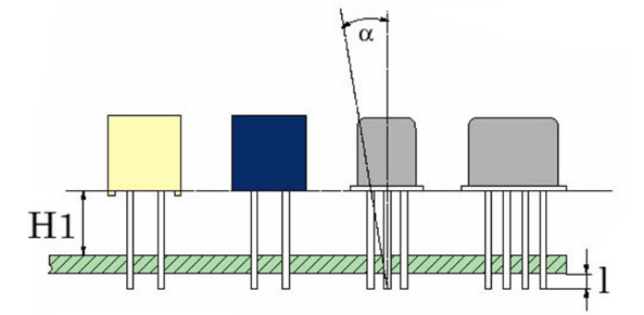
|
Mounting without spacer: 2,4 mm ≤ H1 ≤ 3 mm
| ||
|
Dimensional limits
| |||
|
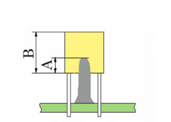
|
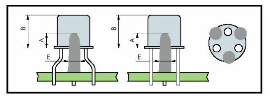
|
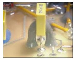
|
|
|
Preferred A > = 1/3 B
|
b) Adhesively staked CKR06
| ||
ECSS-Q-ST-70-61_1510326Figure 8-1: Assembly of TO-39 and CKR06
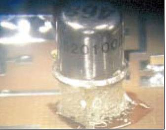 ECSS-Q-ST-70-61_1510327Figure 8-2: TO package with underfill
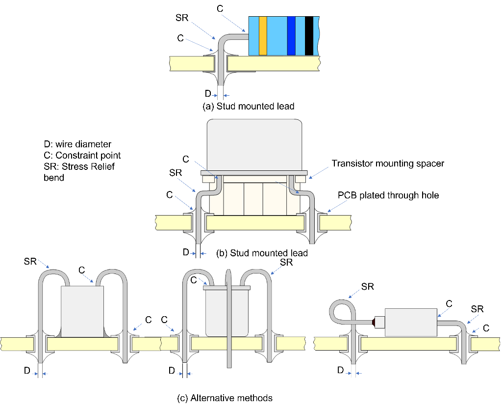 Figure 8-3: Methods for incorporating stress relief with components having bendable leads
Stress relief of components with non-bendable leads
ECSS-Q-ST-70-61_1510328Stress relief for components with non-bendable leads mounted in contact with the PCB or adhesively bonded to the PCB shall use wire extensions according to Figure 8-4.
Bending can damage components when lead diameters are large, or components have delicate seals or where lead-material composition makes bending impracticable.
ECSS-Q-ST-70-61_1510329Dual in Line Package components shall assembled such that tapered portions of the leads are clear of solder.
To achieve acceptable stand-off, a shim can be used
ECSS-Q-ST-70-61_1510330Dual in Line Package components with more than 24 leads shall be assembly verified in accordance with clause 13.
ECSS-Q-ST-70-61_1510331Components sensitive to vibrations and shock tests shall not be assembled as described in requirement 8.2.6a.
Examples of such sensitive components are: relays, oscillators, crystals. ECSS-E-HB-32-25A is providing a list of components known as sensitive to vibration and shock.
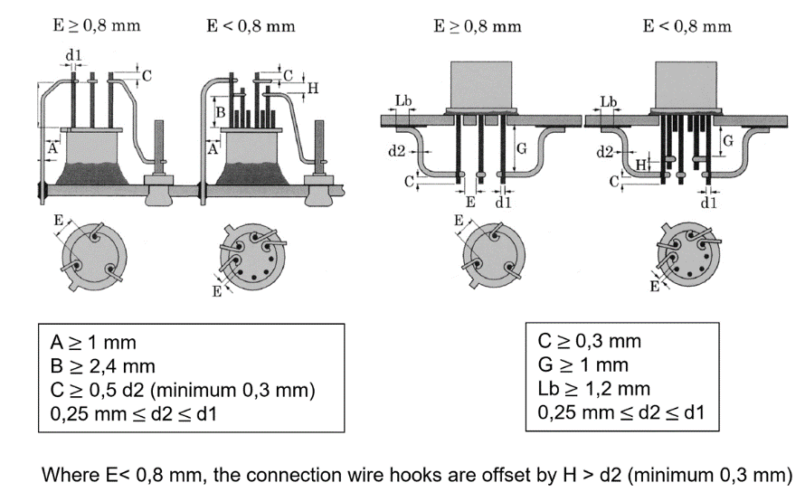 ECSS-Q-ST-70-61_1510332Figure 8-4: Methods for attaching wire extensions to non-bendable leads
Bending of component leads
ECSS-Q-ST-70-61_1510333During bending, component leads shall be supported to avoid axial stress and damage to seals or internal bonds.
ECSS-Q-ST-70-61_1510334The inside radius of a bend shall not be less than one time the lead diameter.
ECSS-Q-ST-70-61_1510335The distances between the bends and the end seals at either end of an axial component shall be similar.
ECSS-Q-ST-70-61_1510336The minimum distance from the bend to the end seal shall be two times the lead diameter for round leads in accordance with Figure 8-5(a).
ECSS-Q-ST-70-61_1510337Where the component lead is welded the minimum distance to the bend shall be measured from the weld in accordance with Figure 8-5(b).
Example: Tantalum capacitors.
ECSS-Q-ST-70-61_1510338Bending tools shall not impinge on the weld.
ECSS-Q-ST-70-61_1510339Leads of dual-in-line and other multileaded components may be mechanically re-aligned with each other, prior to assembly provided that the lead to package connection is not subjected to plastic deformation.
Dedicated tool can be used to avoid any deformation in plastic area of the lead to package connection.
ECSS-Q-ST-70-61_1510340Re-alignment of leads described in requirement 8.2.7g shall be documented in PID.
ECSS-Q-ST-70-61_1510341Lead forming shall be symmetrical.
ECSS-Q-ST-70-61_1510342Formed leads shall not be re-bent.
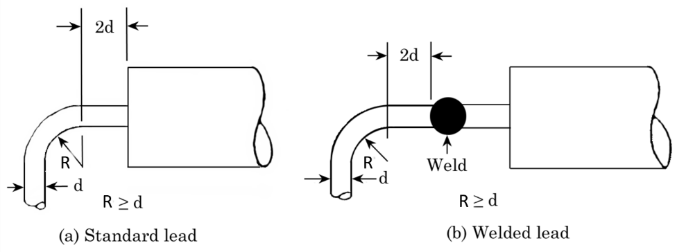 ECSS-Q-ST-70-61_1510343Figure 8-5: Minimum lead bend
Lead attachment to PCBs
General
ECSS-Q-ST-70-61_1510344Direct connection of through hole component leads to PCB shall be performed by stud or clinched lead configuration.
Component leads can be connected with wire extensions with stress relief.
ECSS-Q-ST-70-61_1510345Soldered terminations shall be visible for inspection after soldering.
Stud leads
ECSS-Q-ST-70-61_1510346For PCB thickness less than 2,2 mm, the leads shall protrude beyond the PCB surface by 1,5 mm ± 0,8 mm, as illustrated in Figure 8-6(a).
ECSS-Q-ST-70-61_1510347For components with short leads and PCB thickness greater than or equal to 2,2 mm, the protrusion may be zero, provided that all the following conditions are met:
- the outline of the lead is visible on the solder side,
- there is wetting between the lead and the pad around the entire circumference on solder side according to Figure 8-6(b),
- on the component side, the PCB pad shows solder flow-through and a solder fillet between the lead and the pad on the entire circumference of the lead.
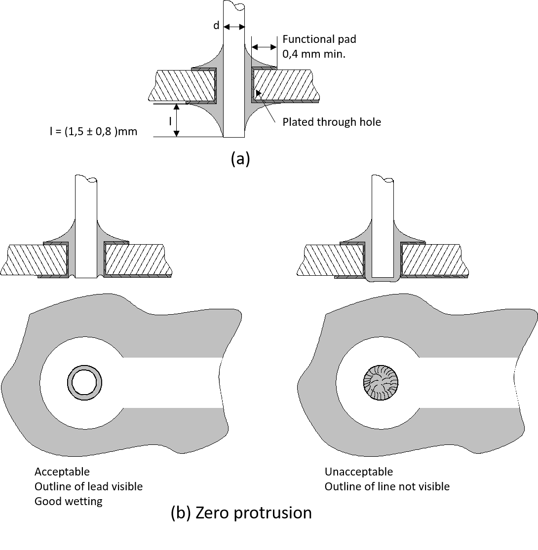 ECSS-Q-ST-70-61_1510348Figure 8-6: Stud leads
ECSS-Q-ST-70-61_1510349For components with procured short leads soldered in plated through holes of thick PCBs negative protrusion shall not be acceptable, unless all the following conditions are met:
- the negative lead protrusion does not exceed 10% of the PCB thickness measured between external laminates.
- the leads are pretinned before soldering, for optimal wetting,
- additional heating from the component side, by means of an extra soldering iron or other preheating system, is applied,
- on the component side, the PCB pad shall show a solder flow-through and a solder fillet between the lead and the pad on the entire circumference of the lead.
- X-ray inspection is carried out after soldering to check the maximum amount of voids is compliant with requirement 12.4a.
Examples of solder flow and voids with X-ray inspection are given in Figure F-1.
Clinching of components in non-plated through holes
ECSS-Q-ST-70-61_1510350Non-bendable leads shall not be clinched.
ECSS-Q-ST-70-61_1510351Clinching shall be performed in accordance with Figure 8-8 and Table 8-1.
ECSS-Q-ST-70-61_1510352Components assembled in non-plated through holes by clinching shall be assembly verified in accordance with clause 13.
Assembly method is defined as SMT configuration with regards to verification.
It is good practice to stake or bond the component with adhesive
ECSS-Q-ST-70-61_1510353For non-plated holes, TO-39 component clinched with stress relief as presented in Figure 8-8 may be mounted without assembly verification.
ECSS-Q-ST-70-61_1510354The lead shall not be forced to lie flat during soldering
Component leads can spring-back when clinched.
ECSS-Q-ST-70-61_1510355The lead shall not be in contact with the PCB at hole corner.
ECSS-Q-ST-70-61_1510356The clinching shall be performed such that:
- the lead extends through and overlap the solder pad,
- the lead is bent to contact the solder pad
- the lead is bent in the direction of the longest dimension of the solder pad, and
- the area of the solder-pad permits a solder fillet to be formed.
ECSS-Q-ST-70-61_1510357No portion of the soldered lead termination shall protrude beyond the pad.
ECSS-Q-ST-70-61_1510358For lapped ribbon leads, one side of the lead may be flush with the edge of the solder pad
ECSS-Q-ST-70-61_1510359For non-plated holes, wires used to connect opposite sides of a PCB shall be clinched with stress relief as presented in Figure 8-7.
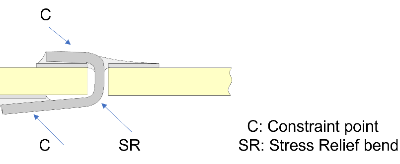 ECSS-Q-ST-70-61_1510360Figure 8-7: Wires used to connect opposite sides of a PCB
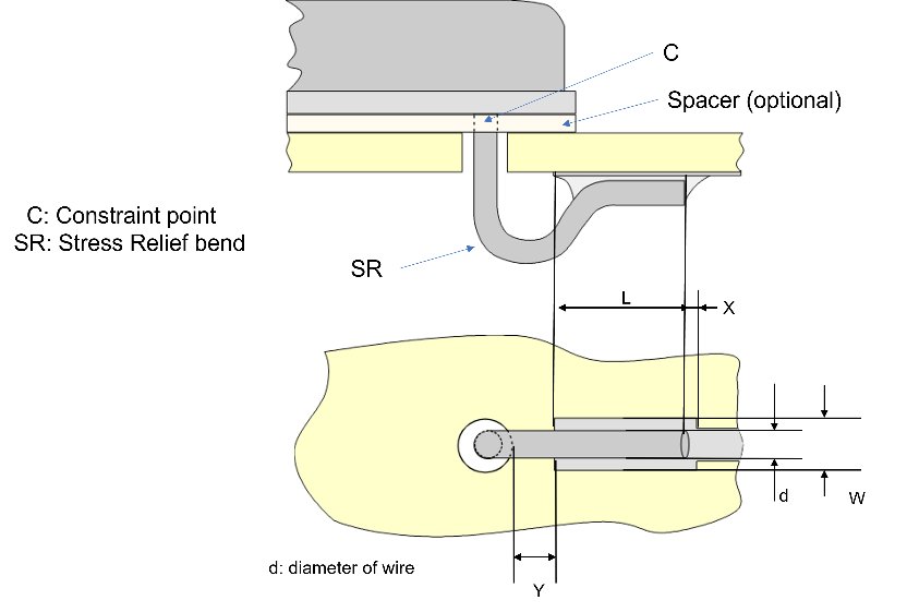 ECSS-Q-ST-70-61_1510361Figure 8-8: Clinching with stress relief for component in non-plated hole
ECSS-Q-ST-70-61_1511127Table 8-1: Dimensions and tolerances for clinching component in non-plated hole
|
Parameter
|
Dimension
|
Dimension limits
|
|
Lead diameter
|
d
|
|
|
Lap connection
|
L
|
4d or 2 mm whichever is smaller
|
|
Minimum distance to footprint edge
|
X
|
0,5 d with 0,25 mm min
|
|
Minimum distance to hole edge
|
Y
|
3d
|
|
Pad width
|
W
|
1,5d min
|
Mounting of through hole connectors to PCBs
ECSS-Q-ST-70-61_1510362PCB connectors shall be supplied with either:
- pre-formed leads supporting stress relief bends, or
- straight, resin moulded connector. ECSS-Q-ST-70-61_1510363Connectors shall be of a configuration incorporating either male or female quick-disconnect contacts and stress relief provision for the soldered connection of each individual contact when such connections are completed
It is good practice to implement a stand-off between solder fillet and component body to insure stress relief.
ECSS-Q-ST-70-61_1510364Connectors outside of what is covered by requirement 8.2.9a may be used providing successful assembly verification in accordance with clause 13.
ECSS-Q-ST-70-61_1510365Degolding and pretinning of leads, in accordance with clause 7.6, shall be performed before mechanical fixing of connectors to the PCB.
ECSS-Q-ST-70-61_1510366Before soldering, the operator shall verify that there will be no contact between the solder fillet to be formed and the gold plating.
ECSS-Q-ST-70-61_1510367Connector leads shall protrude through the board in accordance with clause 8.2.8.2.
Mounting of swage terminals to PCBs
ECSS-Q-ST-70-61_1510368The solder area shall be pretinned in compliance with clauses 7.6.2 or 7.6.3.
ECSS-Q-ST-70-61_1510369Swage-type terminals, designed to have the terminal shoulder soldered to printed conductors, shall be secured to the external layer of a PCB by a roll swage in accordance with Figure 8-9(a).
ECSS-Q-ST-70-61_1510370Swage-type terminals that are mounted in a plated-through hole shall be secured to the PCB by an elliptical funnel swage in accordance with Figure 8-9(b).
An elliptical funnel swage enables complete filling of the plated-through hole with solder.
ECSS-Q-ST-70-61_1510371The PCB shall not be damaged by the swaging process.
ECSS-Q-ST-70-61_1510372After swaging, the terminal shall be inspected for circumferential splits or cracks.
ECSS-Q-ST-70-61_1510373After swaging, the terminal shall be free from circumferential splits or cracks.
ECSS-Q-ST-70-61_1510374After swaging, the terminal may have a maximum of three radial splits or cracks, provided that the splits or cracks do not extend beyond the swaged area of the terminal and are a minimum of 90 apart.
ECSS-Q-ST-70-61_1510375Terminals shall be soldered from swage side and solder flow such that a solder fillet is visible on the opposite side of the terminal.
ECSS-Q-ST-70-61_1510376Terminals shall be soldered using Sn96 to avoid solder to melt whilst wire is soldered on the terminal.
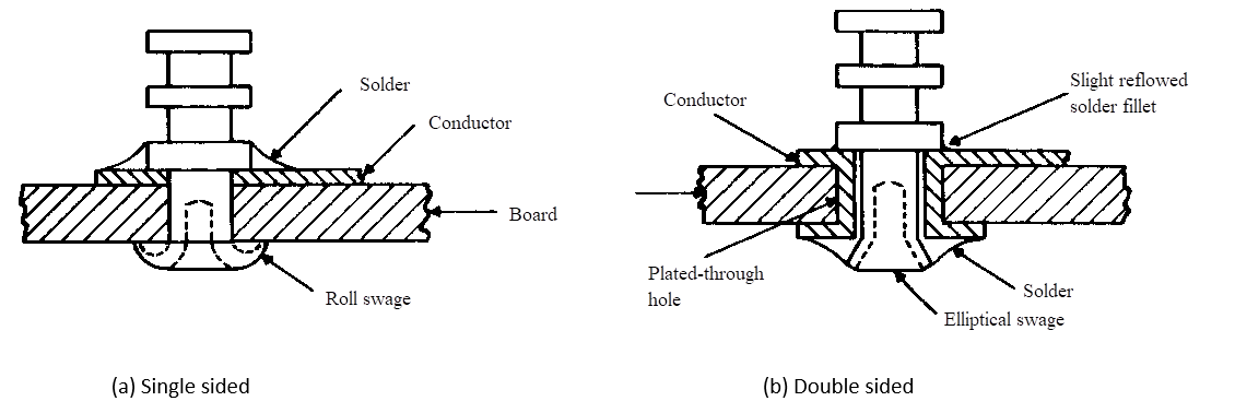 ECSS-Q-ST-70-61_1510377Figure 8-9: Types of terminal swaging
Mounting of components to terminals
ECSS-Q-ST-70-61_1510378Degree of wrap, routing and connection to terminals shall be in accordance with clauses 9 and 10.
ECSS-Q-ST-70-61_1510379The lead length between the component and the terminals shall be similar at both ends, except where component package shapes dictate offset positioning.
Example: Top hat diodes with flanges.
ECSS-Q-ST-70-61_1510380Stress relief shall be provided in accordance with Figure 8-10.
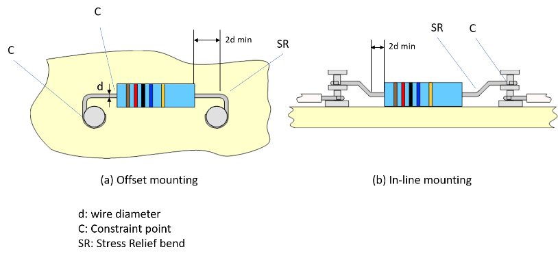 ECSS-Q-ST-70-61_1510381Figure 8-10: Method of stress relieving components attached to terminals
Mounting of surface mount components
General
ECSS-Q-ST-70-61_1510382When CTE mismatch exists between components and substrate, the supplier shall take it into account with the mounting technology.
- 1 Pure eutectic tin-lead solder or indium-lead solder provide better stress relief due to their ductility than those with additional elements, as antimony, gold.
- 2 Leadless components with end-cap terminations, metallization, can have some stress relief (such as additional foil or wire leads, possibly attached by welding or soldered connection.
- 3 A solder stand-off can assist stress relief. In this situation, the CTE mismatch strain is taken up by the ductile solder.
ECSS-Q-ST-70-61_1510383Surface mounting of components shall be parallel to the board surface.
ECSS-Q-ST-70-61_1510384The active element of chip resistors, as illustrated in Figure 8-11, shall be mounted with that surface facing away from the printed circuit board or substrate.
ECSS-Q-ST-70-61_1510385The active element of chip resistors, may be mounted with the active surface facing the printed circuit board or substrate for required electrical performance provided successful assembly verification according to clause 13.
ECSS-Q-ST-70-61_1510386Ceramic chip capacitors may be mounted on the side providing the ratio width:height is less than 1,25:1.
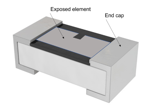 ECSS-Q-ST-70-61_1510387Figure 8-11: Exposed element
Lead forming
ECSS-Q-ST-70-61_1510388The leads of leaded surface mount components shall be formed to their final configuration prior to mounting.
ECSS-Q-ST-70-61_1510389Forming shall not degrade the solderability or cause cracks or loss of plating adhesion to the leads.
ECSS-Q-ST-70-61_1510390Forming shall not cause mechanical damage to the leads or attachment seals.
ECSS-Q-ST-70-61_1510391A maximum of 10 % of section reduction of the lead may be accepted provided that it is representative of the verified configuration and agreed by the Approval Authority.
ECSS-Q-ST-70-61_1510392Leads of gull-wing packages, flat-packs and other multileaded components may be mechanically re-aligned with each other, provided that the lead to package connection is not subjected to plastic deformation and agreed by Approval Authority.
Dedicated tool can be used to avoid any deformation in plastic area of the lead to package connection.
ECSS-Q-ST-70-61_1510393Re-alignment of leads described in 8.3.1d shall be documented in PID.
ECSS-Q-ST-70-61_1510394Lead forming shall be symmetrical.
ECSS-Q-ST-70-61_1510395Formed leads shall not be re-bent.
Inspection of solder paste deposition
ECSS-Q-ST-70-61_1510396The solder paste deposited on each solder footprint shall be inspected for registration and coverage prior to mounting the components.
ECSS-Q-ST-70-61_1510397The inspection shall be performed on the whole surface of the PCB with a microscope or a magnifying tool with a magnification of 4x as a minimum.
ECSS-Q-ST-70-61_1510398Inspection may be performed automatically providing proof of repeatability.
Solder Paste Inspection (SPI) is an example of automatic technic..
ECSS-Q-ST-70-61_1510399The components shall be mounted in solder paste prior to reflow soldering.
Attachment of conductors to terminals, solder cups and cables
General
ECSS-Q-ST-70-61_1510400A conductor shall be wrapped onto a terminal in the same direction as the final curvature of the wire.
ECSS-Q-ST-70-61_1510401Gold-plated terminals and solder cups shall have the gold removed in the conductor attachment area and be pretinned in accordance with clause 7.6.2 and clause 7.6.3.3.
ECSS-Q-ST-70-61_1510402The degolding and pretinning shall be such that the solder joint is not in contact with the gold.
ECSS-Q-ST-70-61_1510403Conductors terminating at solder connections shall incorporate stress relief.
ECSS-Q-ST-70-61_1510404Wicking shall be controlled.
- 1 Anti-wicking tools can be used for pretinning the stranded wires.
- 2 It is good practice to solder one wire per slot.
ECSS-Q-ST-70-61_1510405Terminals and solder cup sizes shall be selected to match the size of conductors in accordance with the manufacturer’s data sheet.
ECSS-Q-ST-70-61_1510406The size of terminals or solder cups shall not be modified.
ECSS-Q-ST-70-61_1510407Insulation clearance shall be in compliance with clause 9.2.2b.
The clearance distance denotes the shortest distance from wire insulation to terminal edge or solder joint whichever is the smallest.”
Wire termination
Breakouts from cables
ECSS-Q-ST-70-61_1510408The length of individual wires routed from a common cable to equally spaced terminals shall be uniform including wire ends and stress-relief bends.
Uniform lengths prevent stress concentration in any one wire.
Insulation clearance
ECSS-Q-ST-70-61_1510409Where characteristic impedance or circuit parameters are not affected, the insulation clearance values stated in clause 7.5.4 shall apply.
ECSS-Q-ST-70-61_1510410Where characteristic impedance or circuit parameters are affected, the insulation clearance requirements may be modified provided that sufficient insulation to surrounding conductive elements is kept.
ECSS-Q-ST-70-61_1510411The modification implemented in requirement 9.2.2b shall be documented in the process procedures.
Example: High-voltage circuits or RF coaxial line terminations.
Turret and straight-pin terminals
ECSS-Q-ST-70-61_1510412Side route connections shall be made as shown in Figure 9-1(a).
- For side route connections, conductors shall be wrapped around the post as shown in Figure 9-1(b):Figure 9-1a minimum of 1/2 turn.
- a maximum of 3/4 turn.
ECSS-Q-ST-70-61_1510413For side route connections to turret terminals, all conductors shall be confined to the guide slots.
ECSS-Q-ST-70-61_1510414For side route connections, conductors shall not project beyond the base of the terminal.
ECSS-Q-ST-70-61_1510415Wires shall not be wrapped over other wires.
ECSS-Q-ST-70-61_1510416More than one wire may be installed in a single slot of a terminal post provided that - the combined diameters of the wires are less than the height of the slot, and
- the contour of each wire is visible.
it is good practice to solder one wire per slot
ECSS-Q-ST-70-61_1510417Wires terminating at terminals that do not have a mechanical shoulder or turret shall not be attached closer than one conductor diameter to the top of the terminal.
ECSS-Q-ST-70-61_1510418Insulation clearance shall be in compliance with clause 9.2.2.
The clearance distance denotes the shortest distance from wire insulation to terminal edge or solder joint whichever is the smallest.”
ECSS-Q-ST-70-61_1510419The solder joints to turret terminals shall meet the solder fillet requirements as illustrated in Figure E-2 and Figure E-3 according to twin or single conductor configuration.
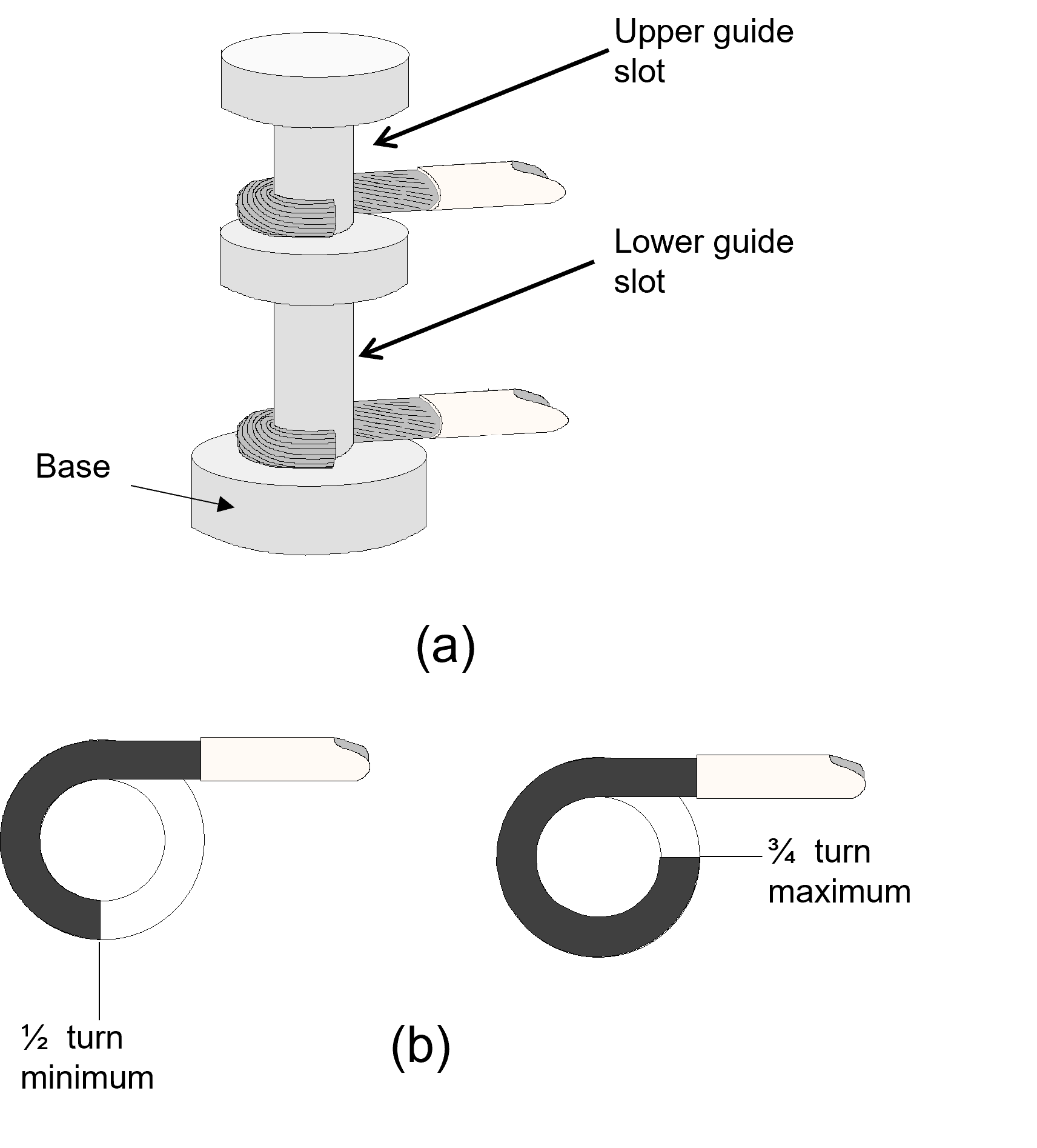 ECSS-Q-ST-70-61_1510420Figure 9-1: Side route connections to turret terminals
Bifurcated terminals
General
ECSS-Q-ST-70-61_1510421Top, side or bottom routes, or combinations thereof, shall be used.
ECSS-Q-ST-70-61_1510422Top route and side route shall not be used together on the same terminal.
Bottom route
ECSS-Q-ST-70-61_1510423Bottom route connections shall be as shown in Figure 9-2(b) and (c).
ECSS-Q-ST-70-61_1510424The conductor shall enter the terminal from the bottom, pass through the side slot at the top, and be wrapped as for the side route, as shown in Figure 9-1(b).
ECSS-Q-ST-70-61_1510425Conductors may project beyond the diameter of the base, see Figure 9-2(c), provided that clearances, environmental and electrical characteristics are not compromised.
ECSS-Q-ST-70-61_1510426The solder joints to bifurcated terminals shall meet the solder fillet requirements as illustrated in Figure E-4.
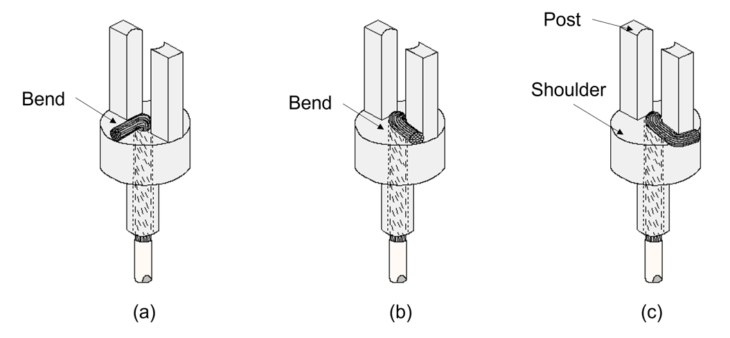 ECSS-Q-ST-70-61_1510427Figure 9-2: Bottom route connections to bifurcated terminal
Side route
ECSS-Q-ST-70-61_1510428Side route connections shall be as shown in Figure 9-3.
ECSS-Q-ST-70-61_1510429The conductor shall enter the mounting slot perpendicular to the posts.
ECSS-Q-ST-70-61_1510430When more than one conductor is connected to a terminal, the direction of bend of each additional conductor shall alternate, see Figure 9-3(b) and (d) with the contour of each wire visible.
ECSS-Q-ST-70-61_1510431Side-route connections shall not project above the top of the terminal.
ECSS-Q-ST-70-61_1510432Conductors may project beyond the diameter of the base, see Figure 9-3(c), provided that clearances, environmental and electrical characteristics are not compromised.
ECSS-Q-ST-70-61_1510433Conductors shall be wrapped a minimum of ¼ turn, as shown in Figure 9-3(a), to a maximum of ½ turn, as shown in Figure 9-3(c) around the post.
ECSS-Q-ST-70-61_1510434The solder joints to bifurcated terminals shall meet the solder fillet requirements as illustrated in Figure E-4.
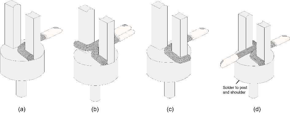 ECSS-Q-ST-70-61_1511128Figure 9-3: Side-route connection to bifurcated terminal
Top route
ECSS-Q-ST-70-61_1510435The top route shall not be used where side entry is possible.
ECSS-Q-ST-70-61_1510436Top route connections shall be as shown in Figure 9-4.
ECSS-Q-ST-70-61_1510437Conductors shall be inserted between the vertical posts to the depth of the shoulder, except for combined top and bottom routes as per clause 9.4.5.
ECSS-Q-ST-70-61_1510438Conductors which do not fill the gap, as shown in Figure 9-4, shall be either:
- accompanied by a tinned filler solid or stranded wire, such that the combined diameters fill the gap, or
- bent double, provided that the combined diameters fill the gap.
ECSS-Q-ST-70-61_1510439The solder joints to bifurcated terminals shall meet the solder fillet requirements as illustrated in Figure E-4.
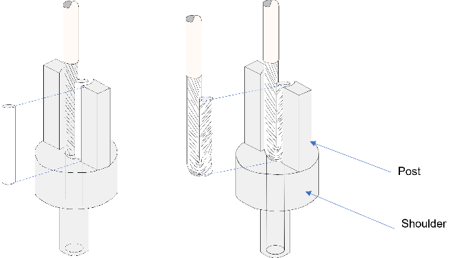 ECSS-Q-ST-70-61_1510440Figure 9-4: Top route connection to bifurcated terminal
Combination of top and bottom routes
ECSS-Q-ST-70-61_1510441The bottom route conductor shall be installed before the top route conductor.
ECSS-Q-ST-70-61_1510442The top route conductor shall be inserted to contact the bottom route conductor.
Combination of side and bottom routes
ECSS-Q-ST-70-61_1510443The bottom route conductor shall be installed before the side route conductor.
Hook terminals
ECSS-Q-ST-70-61_1510444Connections to hook terminals shall be as shown in Figure 9-5.
ECSS-Q-ST-70-61_1510445The bend to attach conductors to hook terminals shall be:
- a minimum of 1/2 turn,
- a maximum of 3/4 turn.
ECSS-Q-ST-70-61_1510446Protrusion of conductor ends shall not damage insulation sleeving.
ECSS-Q-ST-70-61_1510447Where more than one conductor is attached to a terminal, the direction of bend of each conductor shall alternate as shown in Figure 9-5(b).
ECSS-Q-ST-70-61_1510448When more than one conductor is attached to terminal, the conductors shall be at different angles to allow formation of separate solder joints as shown in Figure 9-5(b).
ECSS-Q-ST-70-61_1510449Insulation clearance shall be in compliance with clause 9.2.2.
The clearance distance denotes the shortest distance from wire insulation to terminal edge or solder joint whichever is the smallest.”
ECSS-Q-ST-70-61_1510450The solder joints to hook terminals shall meet the solder fillet requirements as illustrated in Figure E-5.
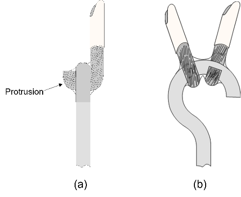 ECSS-Q-ST-70-61_1510451Figure 9-5: Connections to hook terminals
Pierced terminals
ECSS-Q-ST-70-61_1510452Connections to pierced terminals shall be as shown in Figure 9-6.
ECSS-Q-ST-70-61_1510453The bend to attach conductors to pierced terminals shall be:
- a minimum of 1/4 turn,
- a maximum of 3/4 turn.
ECSS-Q-ST-70-61_1510454Protrusion of conductor ends shall not damage insulation sleeving.
ECSS-Q-ST-70-61_1510455Insulation clearance shall be in compliance with clause 9.2.2.
The clearance distance denotes the shortest distance from wire insulation to terminal edge or solder joint whichever is the smallest.”
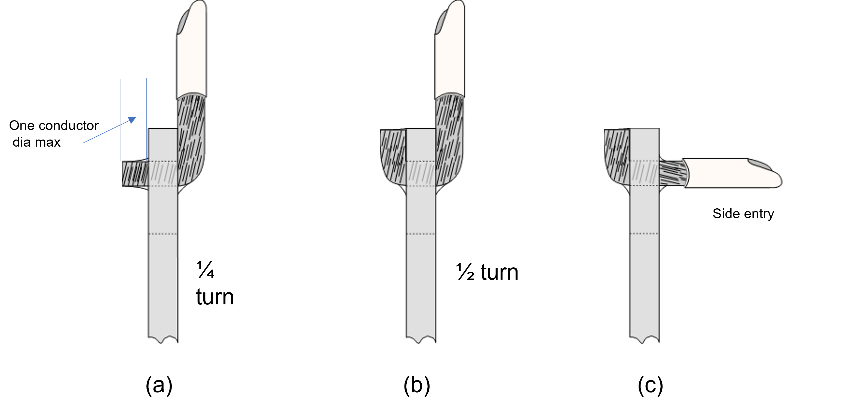 ECSS-Q-ST-70-61_1510456Figure 9-6: Connections to pierced terminals
Solder cups for connector
ECSS-Q-ST-70-61_1510457Conductors shall enter the solder cup as shown in Figure 9-7.
ECSS-Q-ST-70-61_1510458Conductors shall be bottomed in the cup.
ECSS-Q-ST-70-61_1510459Conductors shall be in contact with the inner wall of the cup.
ECSS-Q-ST-70-61_1510460Multiple conductors may be inserted provided that each is in contact with the full height of the inner wall of the cup with contour of each wire visible.
ECSS-Q-ST-70-61_1510461Flux shall not be trapped within the solder cup.
ECSS-Q-ST-70-61_1510462Conductors shall be centred in the terminal and parallel within the contact.
ECSS-Q-ST-70-61_1510463The solder joints to cup terminals shall meet the solder fillet requirements as illustrated in Figure E-6.
ECSS-Q-ST-70-61_1510464Insulation clearance shall be in compliance with clause 9.2.2.
The clearance distance denotes the shortest distance from wire insulation to terminal edge or solder joint whichever is the smallest.”
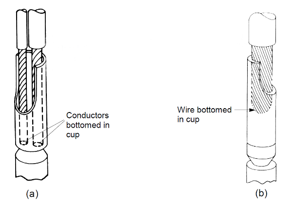 ECSS-Q-ST-70-61_1510465Figure 9-7: Connections to solder cups (connector type)
Insulation sleeving
ECSS-Q-ST-70-61_1510466Electrical connections shall be insulated.
For example with coating, potting, insulation grommets or insulating sleeving.
ECSS-Q-ST-70-61_1510467Heat-shrinkable sleeving shall provide electrical insulation and mechanical support to the finished interconnection.
ECSS-Q-ST-70-61_1510468Interconnection methods shall not use fluxed solder preforms within heat-shrinkable sleeves.
ECSS-Q-ST-70-61_1510469Fluorocarbon sleeves shall not be used.
Fluorocarbon sleeves have high shrinkage temperatures that can damage or reflow soldered connections.
ECSS-Q-ST-70-61_1510470Insulation sleeving shall be transparent and heat shrinkable.
ECSS-Q-ST-70-61_1510471If insulation sleeving is not transparent, inspection of the solder joint shall be done before shrinking the sleeve in place.
ECSS-Q-ST-70-61_1510472A component shall not move within the sleeving when the sleeving is mechanically supported.
ECSS-Q-ST-70-61_1510473The heat-shrinkable insulation sleeving shall be centred over the cleaned and inspected interconnection.
ECSS-Q-ST-70-61_1510474The sleeving shall be cut to a length that covers the finished soldered joint and extends over the remaining insulation of each conductor for a distance of 5 mm ±2 mm.
ECSS-Q-ST-70-61_1510475The minimum overlap between the sleeving and the wire may be shorter than 5 mm ±2 mm. providing minimum overlap is two times the outer wire diameter.
ECSS-Q-ST-70-61_1510476The cut sleeving shall be placed over one of the wires to be joined prior the soldered connection made.
ECSS-Q-ST-70-61_1510477The sleeving shall be shrunk using heated gas or radiant energy.
ECSS-Q-ST-70-61_1510478Heat shrinking of the sleeving shall not damage the assembly.
ECSS-Q-ST-70-61_1510479Heat shall not be applied for more than 8 seconds.
ECSS-Q-ST-70-61_1510480The heat shrinking temperature shall not exceed the maximum temperature recommended by the manufacturer.
ECSS-Q-ST-70-61_1510481The heat-shrinking temperature shall not exceed 140 C at solder joint location.
ECSS-Q-ST-70-61_1510482The minimum distance between hot air blower and shrink sleeving shall be documented by the manufacturer to comply with requirement 9.8o and 9.8p.
ECSS-Q-ST-70-61_1510483PTFE materials shall not be heated above 250 C.
Poisonous gases can be liberated above this temperature.
ECSS-Q-ST-70-61_1510484Flux entrapment within the sleeve shall not be accepted.
Flux residues can be detected by visual inspection.
Wire and cable interconnections
General
ECSS-Q-ST-70-61_1510485Soldered wire interconnection methods shall enable the removal of flux and flux residue.
ECSS-Q-ST-70-61_1510486Soldered wire interconnection methods shall enable visual inspection of the interconnection and surrounding materials.
ECSS-Q-ST-70-61_1510487After soldering, conductors shall be covered with heat-shrinkable sleeving in compliance with clause 9.8.
ECSS-Q-ST-70-61_1510488Enamelled wires with polyimide insulation which have shown susceptibility to cracks shall be heated prior to cleaning to release residual stresses after forming to prevent cracking when cleaning in solvents.
- 1 It is good practice to use a temperature of 125°C for a duration of 2,5 hours.
- 2 When used in magnetics parts, tempering can be part of screening process at component level.
Preparation of wires
ECSS-Q-ST-70-61_1510489Wire insulation shall be removed using insulation strippers in accordance with clause 5.5.6.
ECSS-Q-ST-70-61_1510490Wire insulation clearances shall be in accordance with clause 7.5.4.
ECSS-Q-ST-70-61_1510491Pretinning shall be in accordance with clause 7.6.4.
Preparation of shielded wires and cables
ECSS-Q-ST-70-61_1510492The area of exposed shield shall be either:
- at the end termination of the wire or cable, or
- at any position along the length of a wire or centre splice cable. ECSS-Q-ST-70-61_1510493The insulation jacket as illustrated in Figure 9-8 (a) shall be removed for:
- a minimum length of 5 mm,
- a maximum length of 12 mm. ECSS-Q-ST-70-61_1510494The insulation jacket shall be scored and removed using a sharp cutting tool.
Example: a scalpel.
ECSS-Q-ST-70-61_1510495The preparation process shall not damage the exposed shield material in accordance with clauses 7.5.1 and 7.5.2.
ECSS-Q-ST-70-61_1510496The shield material shall be of good wettability.
ECSS-Q-ST-70-61_1510497The shield material shall not be pretinned.
ECSS-Q-ST-70-61_1510498The shield material shall be cleaned using a solvent in accordance with clause 6.4
Pre-assembly of wires
ECSS-Q-ST-70-61_1510499Conductors shall be secured to prevent disturbance during soldering and solidification using one, or a combination of, the following methods:
- A holding fixture that clamps the wires ensuring correct alignment.
- Rings of heat-shrinkable sleeving positioned over the ends of the wire insulations, see Figure 9-8(b) and (c).
ECSS-Q-ST-70-61_1510500The conductors to be joined shall lie parallel and in contact.
ECSS-Q-ST-70-61_1510501A concave fillet of solder shall be present between the terminal and the sides of the conductor.
ECSS-Q-ST-70-61_1510502The contour of the conductor shall be visible after soldering.
ECSS-Q-ST-70-61_1510503Terminals with more than one wire shall have each wire in contact with and soldered to the terminal.
ECSS-Q-ST-70-61_1510504Conductors may be preformed when the cable insulation prevents a parallel lay.
ECSS-Q-ST-70-61_1510505The bending radius of the wire shall be as a minimum 2 times the diameter of the wire except for polyimide insulated wire for which the minimum bending radius is 10 times the diameter.
ECSS-Q-ST-70-61_1510506Bending tools for the preforming of conductors shall be in accordance with clause 5.5.4.
ECSS-Q-ST-70-61_1510507Wires shall be spliced using lap joints.
ECSS-Q-ST-70-61_1510508For shield terminations, the conductor of the grounding wire shall be positioned on the exposed shield.
ECSS-Q-ST-70-61_1510509Insulation overlap shall not be greater than the diameter of the largest conductor of the interconnection as illustrated in Figure E-9.
ECSS-Q-ST-70-61_1510510The solder joints to shielded cables shall meet the solder fillet requirements as illustrated in Figure E-8.
ECSS-Q-ST-70-61_1510511The solder joints to shielded wires shall meet the solder fillet requirements as illustrated in Figure E-9 and Figure E-10.
ECSS-Q-ST-70-61_1510512The solder joint shall have a mechanical aid such as: - A strand of binding wire, wrapped a minimum of 5 turns, as shown in Figure 9-8(a) or
- A twist-splice around the braid, see Figure 9-8(c) or
- A shrinkable sleeve that maintain the two connections to be made.
ECSS-Q-ST-70-61_1510513The minimum solder connection shall be 5 to 8 mm when no binding wire is used
ECSS-Q-ST-70-61_1510514The minimum solder connection shall be 2 mm when binding wire is used.
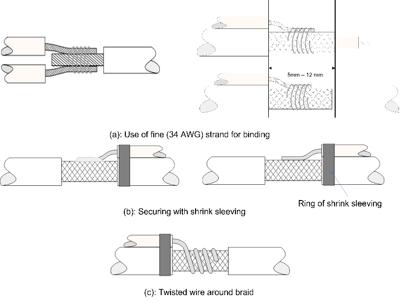 ECSS-Q-ST-70-61_1510515Figure 9-8: Methods for securing wires
Connection of wires to PCBs
ECSS-Q-ST-70-61_1510516Wires shall be soldered to PCB terminations using lap joints or plated-through holes in accordance with Figure 9-9 and Table 9-1.
ECSS-Q-ST-70-61_1510517Stress relief shall be provided.
ECSS-Q-ST-70-61_1510518For PTFE-insulated wire, the minimum distance between the insulation and the solder fillet shall be minimum 1 mm.
ECSS-Q-ST-70-61_1510519The soldered lap connection length L shall be minimum 4d or 2 mm whichever is the smaller as defined in Table 9-1.
ECSS-Q-ST-70-61_1510520Wires shall be supported at maximum 30 mm from stress relief present after the solder joint location and then at intervals not exceeding 50 mm.
ECSS-Q-ST-70-61_1510521Wire support shall be provided by staking, conformal coating or lacing.
ECSS-Q-ST-70-61_1510522The wire shall be embedded in the conformal coating.
As long as the conformal coating is covering a wire, the staking or lacing is not necessary.
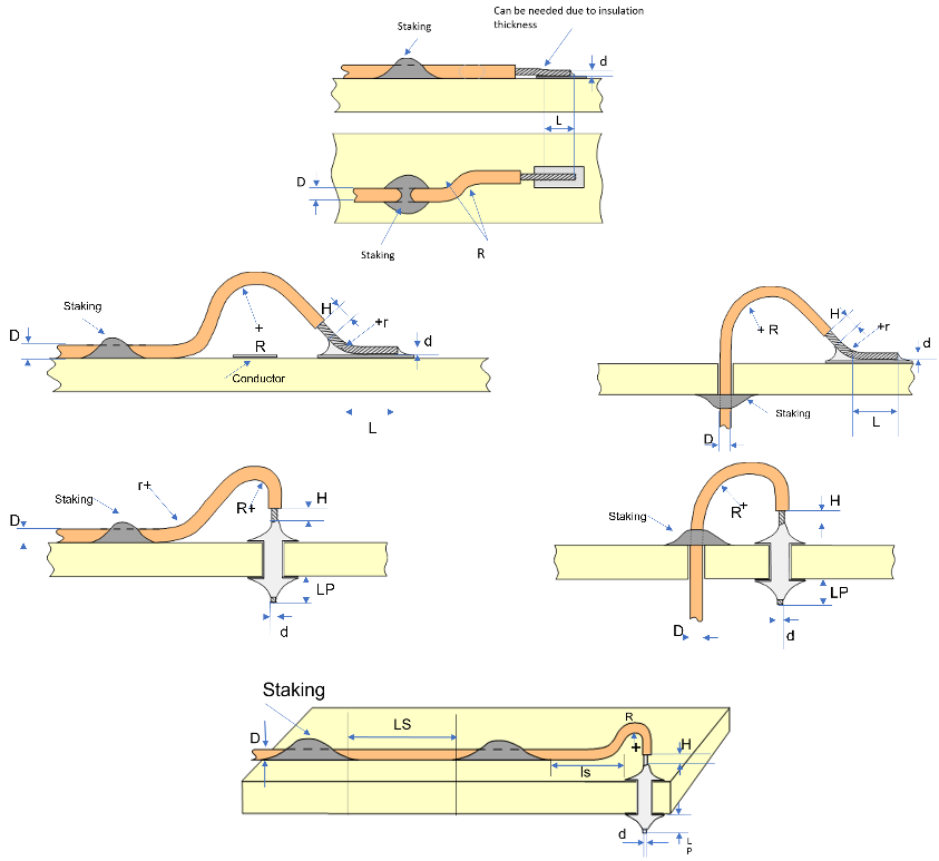 ECSS-Q-ST-70-61_1510523Figure 9-9: Connection of solid or stranded wires to PCBs
ECSS-Q-ST-70-61_1510524Table 9-1: Dimensions for connections of solid or stranded wires to PCBs
|
Parameter
|
Dimension
|
Dimension limits
|
|
Wire bend radius
|
r
|
≥ 2 d
|
|
Conductor bend radius
|
R
|
≥ 2 D general case
|
|
Insulation clearance
|
H
|
1 mm min and according to req. 7.5.4a
|
|
Soldered lap connection length
|
L
|
4d or 2 mm whichever is the smaller
|
|
Lead protrusion through board
|
LP
|
1,5 mm ± 0,8 mm
|
|
Distance between first staking point and soldered connection to PCB
|
ls
|
≤30 mm
|
|
Distance between supporting points
|
LS
|
≤50 mm
|
|
Conductor diameter
|
d
|
min AWG 33 for solid wire
|
|
Outer wire diameter
|
D
|
|
Connection of coaxial cables to PCBs
ECSS-Q-ST-70-61_1510525Coaxial cables shall be soldered to PCB terminations using plated-through holes or surface mount pads, in accordance with Figure 9-10 and Table 9-2.
ECSS-Q-ST-70-61_1510526Stress relief shall be provided.
ECSS-Q-ST-70-61_1510527Coaxial cables shall be supported at maximum 30 mm from the solder and then at intervals not exceeding 50 mm.
ECSS-Q-ST-70-61_1510528Coaxial cables support shall be provided by staking.
ECSS-Q-ST-70-61_1510529Solder of wire over the shielding shall be made without additional flux
. 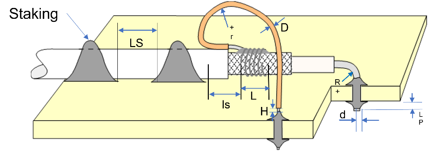
ECSS-Q-ST-70-61_1510530Figure 9-10: Connection of coaxial cables to PCBs
ECSS-Q-ST-70-61_1510531Table 9-2: Dimensions for connections of coaxial cables to PCBs
|
Parameter
|
Dimension
|
Dimension limits
|
|
Wire bend radius
|
r
|
≥ 5 d
|
|
Conductor bend radius
|
R
|
≥ 5 D
|
|
Insulation clearance
|
H
|
1 mm minimum and according to requirement 7.5.4a
|
|
Soldered connection length for wire to shielding braid
|
L
|
2 mm minimum with 5 turns of binding wire
|
|
Lead protrusion through board
|
LP
|
1,5 mm ± 0,8 mm
|
|
Distance between first staking point and soldered connection to PCB
|
ls
|
≤30 mm
|
|
Distance between supporting points
|
LS
|
≤50 mm
|
|
Inner cable conductor diameter
|
d
|
|
|
Shielding wire diameter
|
D
|
min AWG 33 for solid wire
|
Assembly to terminals and to PCBs
Overview
Assembly consists of soldering and solderless technologies.
Soldering technologies are characterized by components or wires that are soldered onto terminals or the PCB with a solder alloy using a soldering process for example solder iron, wave or reflow soldering.
Pressfit connectors are not covered by this standard.
Some components can be assembled without using a soldering process - solderless technology.
Both technologies can co-exist on the same board. In this case, solderless process is the last assembly operation.
General soldering conditions
General
ECSS-Q-ST-70-61_1510532Solders and fluxes shall be selected in accordance with respectively clause 6.2 and clause 6.3
ECSS-Q-ST-70-61_1510533Anti-wicking tool in accordance with clause 5.5.8.4 shall be used to restrict wicking of flux or solder under the wire insulation.
ECSS-Q-ST-70-61_1510534Different solder joints on same component shall be homogenous in volume.
Figure 10-4 to Figure 10-16 show minimum and maximum height values on the same component drawing for illustration purpose.
ECSS-Q-ST-70-61_1510535During soldering of leadless components with soldering iron, the soldering tip shall not be in contact with the termination.
ECSS-Q-ST-70-61_1510536The solder fillet shall not be in contact with any remaining gold-plated area on the termination.
ECSS-Q-ST-70-61_1510537Soldering to gold with tin/lead alloys shall not be performed except the cases specified in the requirements, 6.9.2b.
ECSS-Q-ST-70-61_1510538Configurations not compliant with clause 8.2 may be accepted provided successful verification according to clause 13 and acceptance from the Approval Authority
ECSS-Q-ST-70-61_1510539All configurations from clause 10.4, clause 10.6 and clause 10.7 shall be demonstrated by verification in compliance with requirements from clause 13.
ECSS-Q-ST-70-61_1510540Configurations not compliant with clause 10.4, clause 10.6 or clause 10.7 may be accepted provided successful verification according to clause 13 and acceptance from the Approval Authority.
ECSS-Q-ST-70-61_1510541The shape and fillet height of the solder joint on the flight hardware shall be representative of what has been verified.
ECSS-Q-ST-70-61_1510542The solder fillet criteria shall be identified in the workmanship document of the company and listed in the PID.
ECSS-Q-ST-70-61_1510543Verified acceptance criteria shall be documented and used as pass/fail criteria for FM.
Positioning
ECSS-Q-ST-70-61_1510544There shall be no relative motion between conductors and terminals during soldering or solder solidification.
ECSS-Q-ST-70-61_1510545Conductors shall not be temporarily constrained against spring-back force during solder solidification, to prevent residual stresses in the solder joints, leads and terminals.
Residual stresses are produced in the lead material or solder joint.
ECSS-Q-ST-70-61_1510546Components shall not be mounted on flexible substrates.
See definition of flexible PCB in ECSS-Q-ST-70-60.
ECSS-Q-ST-70-61_1510547Components shall not be stacked nor bridge the space between other components or terminals.
ECSS-Q-ST-70-61_1510548Positioning of components shall not reduce the specified minimum electrical clearance to adjacent tracks or other metallized elements in conformance with clause 14.3.2 of ECSS-Q-ST-70-12.
ECSS-Q-ST-70-61_1510549Maximum tilt limit shall not exceed 10° as shown in Figure 10-1 and Figure 10-2 except in the case defined in requirement 10.2.2g.
Tilt is the angle between the PCB plane and the component axis both along length and width.
 ECSS-Q-ST-70-61_1510550Figure 10-1: Maximum tilt for assembled PTH component
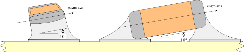 ECSS-Q-ST-70-61_1510551Figure 10-2: Maximum tilt for assembled SMD component
ECSS-Q-ST-70-61_1510552For assembly sensitive components, the maximum tilt shall be defined based on the assembly verification results and not exceed 10°
ECSS-Q-ST-70-61_1510553All leaded components shall be mounted with all leads soldered on a terminal area to provide mechanical strength.
ECSS-Q-ST-70-61_1510554The component positioning shall be such that visual inspection can be undertaken.
ECSS-Q-ST-70-61_1510555If visual inspection of a fully populated assembly is not possible, the assembly and inspection shall be made in steps enabling visual inspection.
Application of flux
ECSS-Q-ST-70-61_1510556External flux shall be used for soldering with the exception of some cases such as soldering on a shielding, pointing of leads of bonded components, assembly of some detectors if cleaning is not possible.
ECSS-Q-ST-70-61_1510557The quantity of flux used shall be such that the solder joint is in accordance with clause 12.
ECSS-Q-ST-70-61_1510558When flux-cored solder is used, it shall be positioned such that the flux flows and covers the components to be joined as the solder melts.
ECSS-Q-ST-70-61_1510559When an external liquid flux is used in conjunction with flux-cored solders, the fluxes shall be compatible.
ECSS-Q-ST-70-61_1510560When external flux is used, liquid flux shall be applied to the surfaces to be joined prior to the application of heat.
Flux controls for wave-soldering equipment
ECSS-Q-ST-70-61_1510561A controlled method shall be established and implemented for wave-soldering machines such that the flux is not contaminated with remaining residues from previous works.
ECSS-Q-ST-70-61_1510562All fluxes properties shall be controlled, and results recorded prior to soldering.
For example, specific gravity.
ECSS-Q-ST-70-61_1510563Dross (oxides) from the solder bath shall be removed so that dross does not mix with the liquid solder.
Automatic or manual processes are acceptable, provided that the dross does not come in contact with the PCB assembly during any portion of the soldering process.
ECSS-Q-ST-70-61_1510564Dross removal material that melt, dissolve or alloy with the liquid solder and flux shall not be used.
Soldering temperatures
ECSS-Q-ST-70-61_1510565For soldering of electronic components, the soldering-tip temperature shall be between 280 C and 340 C except for the cases specified in requirements 10.2.5c, 10.2.5h and 10.2.5p.
- 1 Based on the component manufacturer’s recommendations, solder iron can be substituted by applying, for instance, hot air to avoid thermal shock.
- 2 Ceramic chip capacitors type II are highly prone to cracks in the ceramic. It has been demonstrated that the risk of cracks at completion of a verification programme is reduced by application of gentle soldering conditions where the thermal shock is minimized. It is therefore good practice to:
- Preheat the components to max 120 °C; before soldering
- Preheat the PCB to max 100°C before soldering. Lower if there is adhesive in the area to be preheated;
- Handle the preheated capacitors with thermally insulated tweezer tips;
- Soldering tip temperature of max 260 °C;
- Soldering duration of max 5 seconds;
- If the PCB pads are connected to high thermal mass it might be necessary to increase the soldering temperature to allow proper solder joint formation without increase of the duration.
ECSS-Q-ST-70-61_1510566The soldering temperature may be increased in case the PCB pads are connected to high thermal mass, for component that request assembly verification, provided successful assembly verification in accordance with clause 13.
ECSS-Q-ST-70-61_1510567For PTH connections, the maximum soldering temperature shall be set to, depending on the substrate: - Epoxy: 330 C.
- Polyimide: 340 C
ECSS-Q-ST-70-61_1510568For PTH, a soldering tip temperature up to 380 C may be used for polyimide PCBs with heat sinks, wide tracks, or ground planes.
ECSS-Q-ST-70-61_1510569A soldering tip temperature lower than 280 C may be used for thermal sensitive components.
ECSS-Q-ST-70-61_1510570Thermal shunts, as specified in clause 5.5.8.3, shall be used during soldering to protect thermally-sensitive components.
Example: Conductors, insulation, previously soldered connections and a non-exhaustive list of thermal sensitive components is given hereafter:
- PS Capacitors according to MIL-PRF-49470
- CSR Tantalum Capacitors according to MIL-PRF-39003
- CRH capacitors according to MIL-PRF-83421
- Filters according to MIL-PRF-28861
- Coils according to MIL-PRF-39010
- Resistor Networks according to MIL-PRF-55342
- Thermistors according to MIL-PRF-23648
- Thermistors according to GSFC spec. S-311-P-18.
ECSS-Q-ST-70-61_1510571The use of thermal shunts shall not disturb or damage the solder joint, component or assembly.
ECSS-Q-ST-70-61_1510572In order to improve solder flow, by order of preference, the following actions shall be taken into account: - Select proper solder tip and solder equipment power,
- Introduce preheating of assembly,
- Increase preheating temperature,
- Increase solder temperature.
ECSS-Q-ST-70-61_1510573The soldering iron tip shall be pretinned in accordance with clause 7.7.
ECSS-Q-ST-70-61_1510574The soldering iron tip shall heat the joint area to the solder liquidus temperature in a time between 1 second and 2 seconds.
ECSS-Q-ST-70-61_1510575The soldering iron tip shall maintain the soldering temperature at the joint throughout the soldering operation.
ECSS-Q-ST-70-61_1510576The heated soldering iron tip shall be applied to the PCB pad.
ECSS-Q-ST-70-61_1510577If the thermal dissipation in the PCB is too high during plated through hole soldering, additional heating may be used to be able to achieve an acceptable solder joint on the component side. - 1 Too high thermal dissipation can be due to high thermal masses or locally adjacent heat sinks.
- 2 Additional heating can be applied by pre-heating of the PCB or application of heat to both sides of the plated-through hole simultaneously.
ECSS-Q-ST-70-61_1510578Additional heating shall not damage the components or materials.
ECSS-Q-ST-70-61_1510579The process of additional heating shall be documented.
ECSS-Q-ST-70-61_1510580Soldering temperatures on component terminations shall not exceed the manufacturer recommendations.
ECSS-Q-ST-70-61_1510581The supplier may exceed the component manufacturer's mandated processing conditions providing the following conditions are met: - successful assembly verification in accordance with clause 13,
- dedicated tests at component level showing there is no degradation of these components, and
- customer approval. ECSS-Q-ST-70-61_1510582Components unable to withstand machine soldering temperatures shall be hand soldered in a subsequent operation according to clause 10.3.1.
To mount component by hand soldering at very low temperature can degrade reliability of component and PCB by increasing the duration of soldering necessary to obtain an acceptable solder joint.
Soldering of conductors in terminals
Soldering of conductors onto terminals except cup terminals
ECSS-Q-ST-70-61_1510583A concave fillet of solder shall be present between the terminal and the sides of the conductor.
ECSS-Q-ST-70-61_1510584The contour of the conductor shall be visible after soldering.
ECSS-Q-ST-70-61_1510585Terminals with more than one wire shall have each wire in contact with and soldered to the terminal.
The size of the terminal is selected to fit the number of wires to be soldered. The number of wires is limited so that the contour of the wire is visible and each wire has its own solder joint.
Soldering of conductors onto cup terminals
ECSS-Q-ST-70-61_1510586The solder shall form a fillet between the conductor and the cup entry slot.
ECSS-Q-ST-70-61_1510587The fillet shall follow the contour of the cup opening.
ECSS-Q-ST-70-61_1510588The wire shall be in contact with the bottom of the cup to ensure that the solder length is sufficient.
Soldering of components, terminals, and wires into PCB through holes
General
ECSS-Q-ST-70-61_1510589Soldering of component and wires into plated through holes shall be performed with soldering iron or wave soldering or selective wave soldering.
ECSS-Q-ST-70-61_1510590Solder wire shall be applied only from the solder side of a plated through hole.
ECSS-Q-ST-70-61_1510591Soldering of components into plated through holes may be performed by pin-in-paste method, provided the following conditions are met:
- Solder fillets are compliant to clause 10.3.3.
- Successful verification programme according to clause 13 has been carried out, where the repeatability of the pin-in-paste process is also demonstrated.
- 1 It is good practice to define process design guidelines for solder volume as a function of both pin geometry and volume of plated through hole, so that proper filling of the hole can be achieved.
- 2 If solder paste volume is not sufficient, solder preforms can also be added.
ECSS-Q-ST-70-61_1510592Solder may be applied on the component side of a plated through hole in case pin-in-paste when the method according to requirement 10.3.1c is used.
Solder fillets for wires and terminations
ECSS-Q-ST-70-61_1510593The molten solder shall flow around the termination and over the PCB pad.
ECSS-Q-ST-70-61_1510594Solder amount shall be such that the contour of the wire is visible after soldering.
ECSS-Q-ST-70-61_1510595Soldering of wires shall be performed with stress relief.
ECSS-Q-ST-70-61_1510596If the wire bends from the PCB pad, the lap termination shall have a heel fillet.
Solder fillets for component leads in plated or non-plated through holes
ECSS-Q-ST-70-61_1510597On the solder side, the molten solder shall flow around the termination and over the PCB pad.
ECSS-Q-ST-70-61_1510598On the solder side, leads shall protrude through the board in accordance with clause 8.2.8.2.
ECSS-Q-ST-70-61_1510599On the component side, the PCB pad shall show solder flow-through and a solder fillet between the lead and the pad for a minimum of 75 % of the circumference of the lead as illustrated in Figure 10-3(a).
ECSS-Q-ST-70-61_1510600Absence of component side wetting, due to high thermal dissipation, may be accepted when acceptable solder wetting is visible inside the plated-through hole, on the hole barrel and on the lead, and the solder flow-through is minimum 90 % of PTH (laminate to laminate) as illustrated in Figure 10-3(b).
ECSS-Q-ST-70-61_1510601In case requirement 10.3.3d cannot be verified by visual inspection, the solder joint may be accepted provided X-ray inspection is carried out and conforms to the following two criteria:
- compliance to requirement 12.4a, and
- the solder flow through is minimum 90 %.
- 1 Solder wetting is difficult to assess with X-ray, therefore voids are taken into account.
- 2 Examples of minimum acceptable solder flow through and maximum voids during X-ray are shown in Figure F-1.
ECSS-Q-ST-70-61_1510602If the solder flow-through is less than 90 %, the component assembly shall be verification tested in compliance with requirements from clause 13.
ECSS-Q-ST-70-61_1510603The solder joints to stud terminals shall meet the solder fillet requirements as illustrated in Figure E-1.
ECSS-Q-ST-70-61_1510604The solder fillets for clinched leads shall meet the visual workmanship standards as illustrated in Figure E-2.
ECSS-Q-ST-70-61_1510605The solder fillet for clinched leads shall be in accordance with the visual criteria for gull-wing leads in accordance with clause 10.4.10.
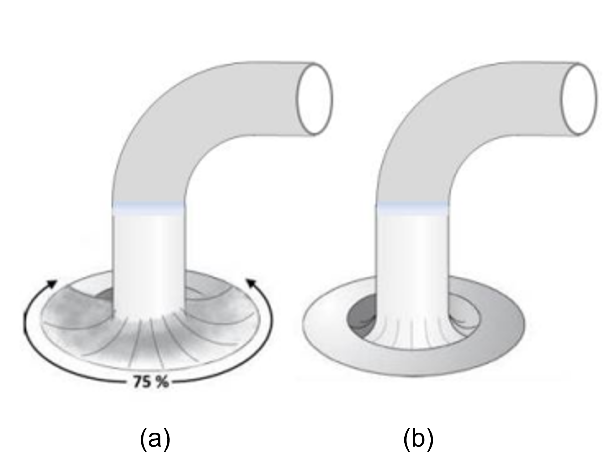 ECSS-Q-ST-70-61_1510606Figure 10-3: Minimum acceptable wetting on component side
Soldering of surface mount components
General
ECSS-Q-ST-70-61_1510607The footprint shall be such that
- the entire termination of the component lies on its associated footprint on the finished board.
- the requirements per component type from clause 10.4.2 to 10.4.14 can be fulfilled.
- the pad size permits the assembly of hand soldering, when applicable, without touching the component.
- 1 to item 3: It is good practice to increase the pad size to facilitate wires soldering in case of modifications.
- 2 to item 3: It is good practice to take into account the surrounding components on the PCB to allow access to the solder pad with the solder tip.
ECSS-Q-ST-70-61_1510608The component shall be centred on its footprints such as the minimum termination contact length is fulfilled.
ECSS-Q-ST-70-61_1510609Solder fillet shall be present on the four sides of the lead.
ECSS-Q-ST-70-61_1510610Solder fillet shall show acceptable wetting on all visible sides.
Some components do not have solder fillet on the sides because of the manufacturing process: for example exposed leadframe as for L-shape Inwards package.
ECSS-Q-ST-70-61_1510611On lap terminations where one side of a conductor is flush with the edge of the termination pad, a fillet of solder shall be present along at least 3 (three) of the four sides of the lead and evidence of acceptable wetting on the side without solder fillet.
ECSS-Q-ST-70-61_1510612The entire component termination shall be wetted.
ECSS-Q-ST-70-61_1510613In case of mounting with artificial stand-off, the minimum solder stand-off shall be repeatable within ± 50 μm.
The stand-off enables adequate cleaning beneath the assembled LCCC and enhances solder fatigue life.
Rectangular and square end-capped or end-metallized leadless chip
ECSS-Q-ST-70-61_1510614There shall be no discernible discontinuities in the solder coverage of the terminal areas of components.
ECSS-Q-ST-70-61_1510615Solder shall not encase any portion of the body of the component following reflow.
ECSS-Q-ST-70-61_1510616The solder joints to these components shall meet the dimensional and solder fillet requirements of Figure 10-4 and Table 10-1.
- 1 Ceramic chip capacitors or resistors, ceramic resistor arrays and metallic chip components such as CSM2512 or resistors with metallic terminations such as SMS 2512, ferrites, thermistors and fuses, are all examples of components in this group.
- 2 Convex solder fillet can cause additional stress in the component terminations, therefore convex solder fillets are not recommended. Especially for ceramic chip capacitors it has been demonstrated that a lower wetting height reduces the risk of cracks in the ceramic at the completion of verification.
- 3 Manual soldering, especially with artificial stand-off can make it difficult to fulfil maximum side overhang and minimum termination contact lengths.
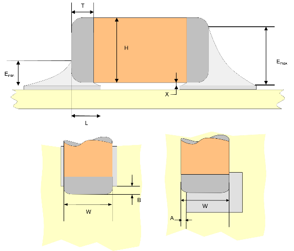 ECSS-Q-ST-70-61_1510617Figure 10-4: Mounting of rectangular and square end-capped and end-metallized components
ECSS-Q-ST-70-61_1510618Table 10-1: Dimensional and solder fillet for rectangular and square end capped components
|
Parameter
|
Dimension
|
Dimension limits
|
|
Maximum side overhang
|
A
|
0,1 × W
|
|
End overhang
|
B
|
Not permitted
|
|
Minimum termination contact length
|
L
|
0,75 × T on one end of the component only
|
|
Minimum fillet height
|
Emin
|
X + 0,3 × H or X + 0,5 mm whichever is less
|
|
Minimum fillet width
|
W-A
|
100% × W or
|
|
Maximum fillet height*
|
Emax
|
*: only for chip capacitor Emax ≤H
|
|
Solder Stand-off (elevation)
|
X
|
Present
|
|
Maximum tilt limit
|
in accordance with requirement 10.2.2f
|
|
|
Termination width
|
W
|
|
|
Component height
|
H
|
|
|
Termination length
|
T
|
|
Cylindrical and square end-capped components with cylindrical or oval body
ECSS-Q-ST-70-61_1510619Solder joints to components having cylindrical terminations shall meet the dimensional and solder fillet requirements of Figure 10-5 and Table 10-2.
ECSS-Q-ST-70-61_1510620Solder joints to components having square terminations shall meet the dimensional and solder fillet requirements of Figure 10-6 and Table 10-3.
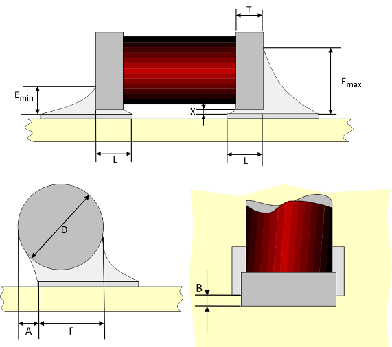 ECSS-Q-ST-70-61_1510621Figure 10-5: Mounting of cylindrical end-capped components
ECSS-Q-ST-70-61_1510622Table 10-2: Dimensional and solder fillet for cylindrical end-capped components
|
Parameter
|
Dimension
|
Dimension limits
|
|
Maximum side overhang
|
A
|
0,25 D (diameter)
|
|
End overhang
|
B
|
Not permitted
|
|
Minimum fillet width
|
F
|
0,5 D
|
|
Minimum fillet height
|
Emin
|
X + 0,3 D or
|
|
Maximum fillet height
|
Emax
|
D
|
|
Minimum termination contact length
|
L
|
0,75 T on one end of the component only
|
|
Stand-off (elevation)
|
X
|
Present
|
|
Maximum tilt limit
|
in accordance with requirement 10.2.2f
|
|
|
Termination diameter
|
D
|
|
|
Termination length
|
T
|
|
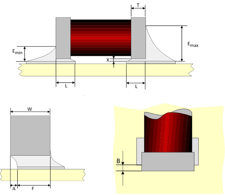 ECSS-Q-ST-70-61_1510623Figure 10-6: Mounting of square end-capped components
ECSS-Q-ST-70-61_1510624Table 10-3: Dimensional and solder fillet for square end-capped components
|
Parameter
|
Dimension
|
Dimension limits
|
|
Maximum side overhang
|
A
|
0,25 W (square width)
|
|
End overhang
|
B
|
Not permitted
|
|
Minimum fillet width
|
F
|
0,75 W
|
|
Minimum fillet height
|
Emin
|
X + 0,3 W or
|
|
Maximum fillet height
|
Emax
|
W
|
|
Minimum termination contact length
|
L
|
0,75 T on one end of the component only
|
|
Stand-off (elevation)
|
X
|
Present
|
|
Maximum tilt limit
|
in accordance with requirement 10.2.2f
|
|
|
Termination length
|
T
|
|
|
Termination width
|
W
|
|
Bottom terminated chip components
ECSS-Q-ST-70-61_1510625Devices having metallized terminations on the bottom side only shall meet the dimensional and solder fillet requirements of Figure 10-7 and Table 10-4.
Examples of components from this family are SMD coils.
ECSS-Q-ST-70-61_1510626Solder fillet shall show acceptable wetting on all visible sides.
ECSS-Q-ST-70-61_1510627Assembly shall be inspected with X-ray according to criteria defined in requirement 12.4a when solder fillet is not visible.
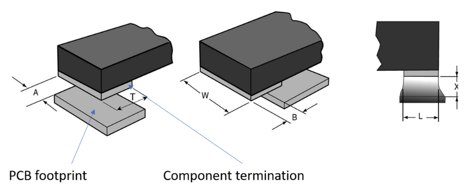 ECSS-Q-ST-70-61_1510628Figure 10-7: Mounting of bottom terminated chip component
ECSS-Q-ST-70-61_1510629Table 10-4: Dimensional and solder fillet for bottom terminated chip components
|
Parameter
|
Dimension
|
Dimension limits
|
|
Maximum side overhang
|
A
|
0,1 W
|
|
End overhang
|
B
|
Not permitted
|
|
Minimum termination contact length
|
L
|
0,75 T on one end of the component only
|
|
Minimum fillet width
|
W-A
|
100% W or
|
|
Solder Stand-off (elevation)
|
X
|
Present
|
|
Maximum tilt limit
|
in accordance with requirement 10.2.2f
|
|
|
Termination width
|
W
|
|
|
Termination length
|
T
|
|
L-Shape inwards components
ECSS-Q-ST-70-61_1510630Components having L-shape inwards terminals shall meet the dimensional and solder fillet requirements of Figure 10-8 and Table 10-5.
ECSS-Q-ST-70-61_1510631Solder fillet shall show acceptable wetting on all visible sides.
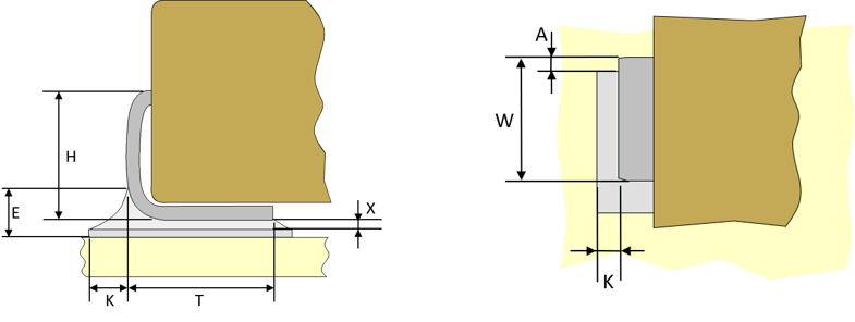 ECSS-Q-ST-70-61_1510632Figure 10-8: Mounting of components with “L-shape inwards” leads
ECSS-Q-ST-70-61_1510633Table 10-5: Dimensional and solder fillet for “L-shape inwards” components
|
Parameter
|
Dimension
|
Dimensions limits
|
|
Maximum side overhang
|
A
|
0,1 × W
|
|
Minimum heel fillet height
|
E
|
(0,25 x H) +X or X +1mm whichever is less
|
|
Minimum fillet width
|
W-A
|
100%xW or
|
|
Minimum distance to footprint edge
|
K
|
0,2 mm
|
|
Minimum termination contact length
|
L
|
0,75 T on one end of the component only
|
|
Stand-off (elevation)
|
X
|
Present
|
|
Lead height
|
H
|
|
|
Lead width
|
W
|
|
|
Termination length
|
T
|
|
Leadless component with plane termination
ECSS-Q-ST-70-61_1510634Leadless components with plane termination shall meet the dimensional and solder fillet requirements of Figure 10-9 and Table 10-6.
Leadless components with plane termination can have a metallic plane or non-metallic plane termination.
ECSS-Q-ST-70-61_1510635 Solder fillet shall show acceptable wetting on all visible sides.
ECSS-Q-ST-70-61_1510636Assembly shall be inspected with X-ray according to criteria defined in requirement 12.4a when solder fillet is not visible.
ECSS-Q-ST-70-61_1510637When either thermal or electrical ground performances are requested, terminal plane shall be inspected with X-ray according to criteria defined in requirement 12.4a.
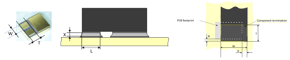 ECSS-Q-ST-70-61_1510638Figure 10-9: Mounting of leadless component with plane termination
ECSS-Q-ST-70-61_1510639Table 10-6: Dimensional and solder fillet for leadless component with plane termination
|
Parameter
|
Dimension
|
Dimension limits
|
|
Maximum side overhang
|
A
|
0,1 W providing minimum insulation distance remains acceptable.
|
|
End overhang
|
B
|
Not permitted
|
|
Minimum termination contact length
|
L
|
Entire termination of component T
|
|
Minimum fillet width
|
W-A
|
100% W or
|
|
Solder Stand-off (elevation)
|
X
|
Present
|
|
Maximum tilt limit
|
in accordance with
|
|
|
Termination width
|
W
|
|
|
Termination length
|
T
|
|
Leaded component with plane termination
ECSS-Q-ST-70-61_1510640Leaded components with plane termination shall meet the dimensional and solder fillet requirements of Figure 10-10 and Table 10-7.
ECSS-Q-ST-70-61_1510641 Solder fillet shall be present on the visible edge of the terminal plane.
ECSS-Q-ST-70-61_1510642Terminal plane shall be inspected with X-ray according to criteria defined in requirement 12.4a.
 ECSS-Q-ST-70-61_1510643Figure 10-10: Mounting of leaded components with plane termination
ECSS-Q-ST-70-61_1510644Table 10-7: Dimensional and solder fillet for leaded components with plane termination
|
Parameter
|
Dimension
|
Dimension limits
|
|
Maximum side overhang
|
A
|
0,1 W
|
|
Minimum distance to footprint edge at toe
|
B
|
0,20 mm
|
|
Minimum distance to footprint edge at heel
|
K
|
0,5 W
|
|
Minimum heel fillet height
|
E
|
X + T
|
|
Minimum fillet width
|
W-A
|
100% W or
|
|
Solder Stand-off
|
X
|
Present
|
|
Lead thickness
|
T
|
|
|
Lead width
|
W
|
|
Leadless castellated ceramic chip carrier components
ECSS-Q-ST-70-61_1510645Solder joints to leadless castellated ceramic chip carrier terminations shall meet the dimensional and solder fillet requirements of Figure 10-11 and Table 10-8.
It can be difficult to assess the wetting in X-ray, but solder joints with deviating shape or amount compared to the neighbouring connections indicate that a closer look is needed.
ECSS-Q-ST-70-61_1510646Exposed pad shall be inspected with X-ray according to criteria defined in requirement 12.4a.
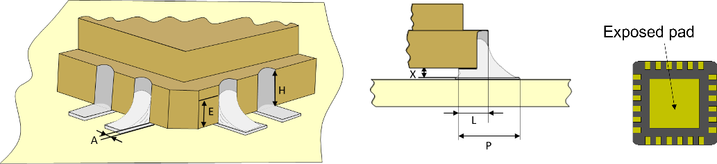 ECSS-Q-ST-70-61_1510647Figure 10-11: Mounting of leadless castellated ceramic chip carrier components
ECSS-Q-ST-70-61_1510648Table 10-8: Dimensional and solder fillet for leadless castellated ceramic chip carrier components
|
Parameter
|
Dimension
|
Dimension limits
|
|
Maximum side overhang
|
A
|
Not permitted
|
|
Minimum fillet height
|
E
|
0,75 H
|
|
Minimum fillet width
|
-
|
100% termination width
|
|
Solder Stand-off (elevation)
|
X
|
Present
|
|
Minimum termination contact length
|
L
|
Entire termination of component
|
|
Castellation metallisation height
|
H
|
|
|
Pad length
|
P
|
|
No lead Quad Flat Pack
ECSS-Q-ST-70-61_1510649Solder joints formed to QFN shall meet the dimensional and solder fillet requirements of Figure 10-12 and Table 10-9.
Presence or absence of external solder fillet is depending on package technology.
ECSS-Q-ST-70-61_1510650Solder fillet shall show acceptable wetting on all visible sides.
ECSS-Q-ST-70-61_1510651Heel solder fillet shall be present.
ECSS-Q-ST-70-61_1510652Assembly shall be inspected with X-ray according to criteria defined in requirement 12.4a when solder fillet is not visible.
ECSS-Q-ST-70-61_1510653When either thermal or electrical ground performances are requested, exposed pad shall be inspected with X-ray according to criteria defined in requirement 12.4a.
ECSS-Q-ST-70-61_1510654X-ray inspection may be omitted providing justification and approval of Approval Authority.
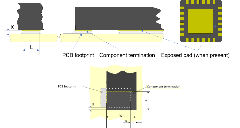 ECSS-Q-ST-70-61_1510655Figure 10-12 Mounting of QFN
ECSS-Q-ST-70-61_1510656Table 10-9: Dimensional and solder fillet for QFN components
|
Parameter
|
Dimension
|
Dimension limits
|
|
Maximum side overhang
|
A
|
Not permitted
|
|
End overhang
|
B
|
Not permitted
|
|
Minimum termination contact length
|
L
|
Entire termination of component
|
|
Solder Stand-off (elevation)
|
X
|
Present
|
|
Solder fillet height
|
H
|
In compliance with verification results
|
|
Minimum fillet width
|
W-A
|
100% W
|
|
Maximum tilt limit
|
in accordance with requirement 10.2.2f
|
|
|
Termination width
|
W
|
|
|
Termination length
|
T
|
|
Flat pack and gull-wing leaded components with round, rectangular, ribbon leads
ECSS-Q-ST-70-61_1510657Solder joints formed to flat pack and gull-wing leaded components with round, rectangular, ribbon leads shall meet the dimensional and solder fillet requirements of Figure 10-13 and Table 10-10.
ECSS-Q-ST-70-61_1510658Solder fillet shall be present on the four sides of the lead.
ECSS-Q-ST-70-61_1510659When exposed pad is soldered, it shall be inspected with X-ray according to criteria defined in requirement 12.4a.
. 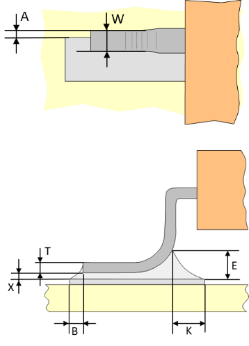
ECSS-Q-ST-70-61_1510660Figure 10-13: Mounting of gull-wing leaded components with round, rectangular, ribbon leads
ECSS-Q-ST-70-61_1511129Table 10-10: Dimensional and solder fillet for gull-wing leaded components with round, rectangular, ribbon leads
|
Parameter
|
Dimension
|
Dimension limits
|
|
Maximum side overhang
|
A
|
0,1 W
|
|
Minimum distance to footprint edge at toe
|
B
|
0,20 mm
|
|
Minimum distance to footprint edge at heel
|
K
|
0,5 W
|
|
Minimum heel fillet height
|
E
|
X + T
|
|
Minimum fillet width
|
W-A
|
100% W or
|
|
Solder Stand-off
|
X
|
Present
|
|
Lead thickness
|
T
|
|
|
Lead width
|
W
|
|
Components with “J” leads
ECSS-Q-ST-70-61_1510661Solder joints formed to “J” and “V” shaped leads shall meet the dimensional and solder fillet requirements of Figure 10-14 and Table 10-11.
ECSS-Q-ST-70-61_1510662The fillet of solder along the lead shall extend up to a minimum distance of half the lead thickness or diameter.
ECSS-Q-ST-70-61_1510663When exposed pad is soldered, it shall be inspected with X-ray according to criteria defined in requirement 12.4a.
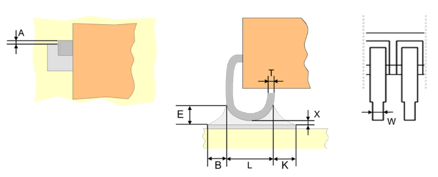 ECSS-Q-ST-70-61_1510664Figure 10-14: Mounting of component with “J” leads
ECSS-Q-ST-70-61_1510665Table 10-11: Dimensional and solder fillet for components with “J” leads
|
Parameter
|
Dimension
|
Dimension limits
|
|
Maximum side overhang
|
A
|
0,1 W
|
|
Minimum termination contact length
|
L
|
100% on the pad
|
|
Minimum heel fillet height
|
Eh
|
X+T
|
|
Minimum toe fillet height
|
Ef
|
X+T
|
|
Minimum fillet width
|
W-A
|
100% W or
|
|
Minimum distance to footprint edge at toe
|
B
|
0,20 mm or 0,5 W whichever is the smaller
|
|
Minimum distance to footprint edge at heel
|
K
|
0,20 mm or 0,5 W whichever is the smaller
|
|
Minimum stand-off
|
X
|
Present
|
|
Lead thickness
|
T
|
|
|
Lead width
|
W
|
|
Components with ribbon terminals without stress relief
ECSS-Q-ST-70-61_1510666Solder joints formed shall meet the dimensional and solder fillet requirements of Figure 10-15 and Table 10-12.
When component dimensions allow, it is good practice to have a minimum termination contact length L of three times the lead width W.
ECSS-Q-ST-70-61_1510667The degolding and pretinning zone shall be larger than the PCB footprint without reducing the clearance distance of the component.
The aim is to prevent soldering to gold plated surfaces.
ECSS-Q-ST-70-61_1510668The fillet of solder along the lead shall extend up the side of the lead to a minimum distance of half the lead thickness or diameter.
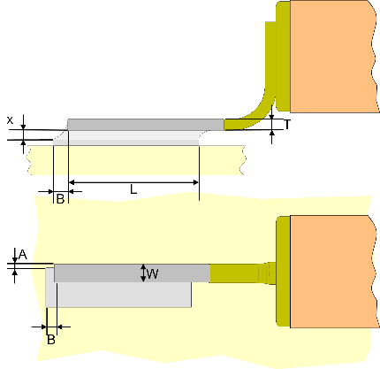 ECSS-Q-ST-70-61_1510669Figure 10-15: Mounting of components without stress relief
ECSS-Q-ST-70-61_1510670Table 10-12: Dimensional and solder fillet for components with ribbon terminals without stress relief
|
Parameter
|
Dimension
|
Dimensions limits
|
|
Maximum side overhang
|
A
|
0,1 W
|
|
Minimum distance to footprint edge at toe
|
B
|
0,20 mm
|
|
Minimum fillet width
|
W-A
|
100% W or
|
|
Stand-off
|
X
|
Present
|
|
Minimum termination contact length
|
L
|
Fully soldered lap connection
|
|
Maximum tilt limit
|
in accordance with requirement 10.2.2f
|
|
|
Lead thickness
|
T
|
|
|
Lead width
|
W
|
|
Stacked modules components with leads protruding vertically from bottom
ECSS-Q-ST-70-61_1510671Stacked module components shall meet the dimensional and solder fillet requirements of Figure 10-16 and Table 10-13.
ECSS-Q-ST-70-61_1510672Solder fillet shall be present on the four sides of the lead.
 ECSS-Q-ST-70-61_1510673Figure 10-16: Mounting of stacked module components with leads protruding vertically from bottom
ECSS-Q-ST-70-61_1510674Table 10-13: Dimensional and solder fillet for stacked module components with leads protruding vertically from bottom
|
Parameter
|
Dimension
|
Dimension limits
|
|
Maximum side overhang
|
A
|
0,1 W
|
|
Minimum distance to footprint edge at toe
|
B
|
0,20 mm
|
|
Minimum distance to footprint edge at heel
|
K
|
0,5 W
|
|
Minimum termination contact length
|
L
|
Entire termination of component
|
|
Minimum heel fillet height
|
E
|
Wetting solder visible in the heel fillet, X+ 0,5T
|
|
Minimum fillet width
|
W-A
|
100% W or
|
|
Solder Stand-off
|
X
|
Present
|
|
Lead thickness
|
T
|
|
|
Lead width
|
W
|
|
Area array devices
ECSS-Q-ST-70-61_1510675The connections of area array devices shall meet the dimensional and solder fillet requirements of Figure 10-17 and Table 10-14.
ECSS-Q-ST-70-61_1510676The outer rows shall be visually inspected.
ECSS-Q-ST-70-61_1510677Solder joints shall be inspected with X-ray according to criteria defined in requirement 12.4a.
- 1 As it is impossible to visually inspect solder joints to area array components, reliability of these components cannot be assured by inspection and rework. Even using X-Ray techniques, some types of defect are difficult to detect. Therefore, reliability of these solder joints can only be assured by robust process control.
- 2 Examples of typical area array components are shown in Figure 10-17.
ECSS-Q-ST-70-61_1510678X-ray techniques shall be used to verify the acceptable wetting, the absence of bridge, solder balls and minimum electrical clearance.
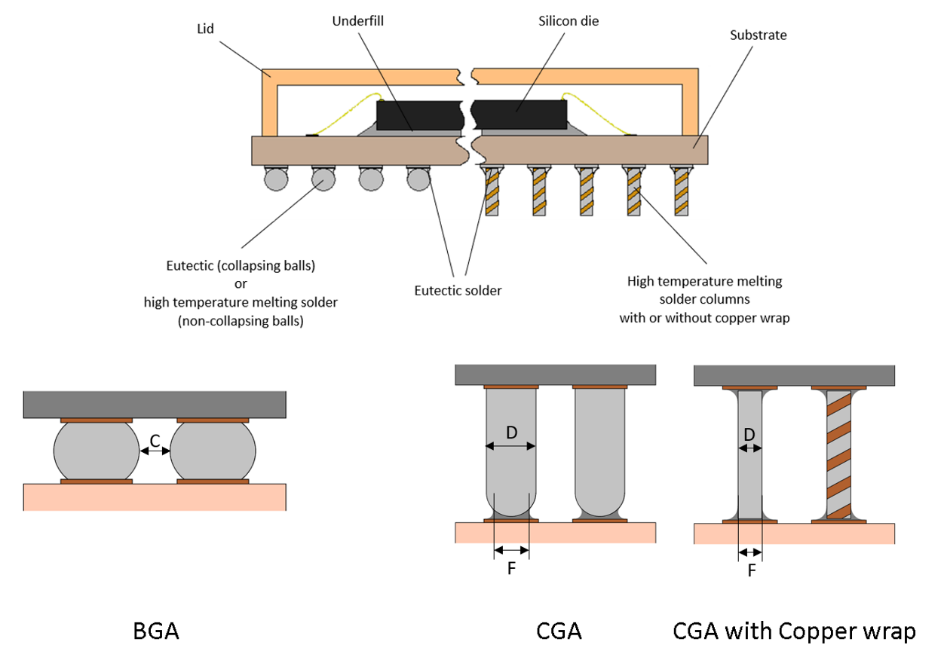 ECSS-Q-ST-70-61_1510679Figure 10-17: Typical configuration of ceramic grid array component
ECSS-Q-ST-70-61_1510680Table 10-14: Dimensional and solder fillet for area array devices
|
|
Parameter
|
Dimension
|
Dimension limits
|
|
General
|
Wetting
|
-
|
All connections show evidence of contact and wetting to its solder land.
|
|
Solder balls
|
-
|
No solder balls
| |
|
BGA
|
Electrical clearance
|
C
|
Electrical clearance is not violated and
|
|
CGA
|
Column tilting
|
-
|
Maximum 10°
|
|
Misalignment
|
-
|
No footprint overhang
| |
|
Minimum fillet width
|
F
|
CGA with rounded bottom column: F ≥ 0,5 D
| |
|
Column diameter
|
D
|
|
Rework and repair
Removal of solder on unpopulated PCB
ECSS-Q-ST-70-61_1510681Removal of solder shall be performed after the board has been submitted to bake out in compliance with clause 7.3.
ECSS-Q-ST-70-61_1510682Rework of plated through holes in PCBs may be performed up to maximum 25 % per component position with a maximum of 3 (three) times for the same plated through hole.
- 1 Plated through holes can be blocked from PCB manufacturer in case of small hole dimensions.
- 2 See also ECSS-Q-ST-70-60 requirement 10.6.3g.
- 3 "3 times" includes rework after assembly.
ECSS-Q-ST-70-61_1510683The number and location of reworks performed according to 10.5.1b shall be recorded in the traveller sheet of the board.
ECSS-Q-ST-70-61_1510684For unpopulated PCB, in case more that 25 % per component position are reworked, the removal of solder shall be classified as a repair and be performed in accordance with ECSS-Q-ST-70-28.
Rework, repair and modifications
ECSS-Q-ST-70-61_1510685Any rework, repair or modifications shall be in accordance with ECSS-Q-ST-70-28 with the exceptions of all requirements of clause 10.5.1 and requirements 10.5.2b to 10.5.2h.
The deviation to ECSS-Q-ST-70-28 comes from the fact that the complexity of electronic components has evolved since the publication of ECSS-Q-ST-70-28. In particular the number of component leads and their density on the board have increased drastically.
ECSS-Q-ST-70-61_1510686Retinnning of PCB pads after component removal shall be done in accordance with requirement 7.6.3.1d.
ECSS-Q-ST-70-61_1510687Rework of soldered PCB assemblies shall be done when the solder joint does not meet the criteria of clause 12.
ECSS-Q-ST-70-61_1510688The total number of solder reworks, including the ones done prior to soldering according to requirement 10.5.1b shall not exceed three times per PCB pad, except in case for epoxy substrates covered by requirement 10.5.2e.
- 1 Epoxy and flex rigid PCB are sensitive to thermal stress induced by rework.
- 2 For reworking, the solder can be completely removed from the termination.
- 3 In case of high thermal mass, it is good practice to have a preheating of components and PCB.
ECSS-Q-ST-70-61_1510689For epoxy substrates, the total number of solder reworks or repair, including the ones done prior to soldering according to requirement 10.5.1b shall not exceed two times per PCB pad.
This means it is allowed to perform either two reworks or one rework and one repair.
ECSS-Q-ST-70-61_1510690The number of reworked solder joints shall not exceed 10 % of the total number of solder joints on a board with the exception specified in requirements 10.5.2g and 10.5.2h.
ECSS-Q-ST-70-61_1510691For boards smaller than 25 cm2 the number of reworked solder joints shall not exceed 25 % of the total number of solder joints on a board.
ECSS-Q-ST-70-61_1510692For components with more than one hundred terminations, the number of reworked solder joints shall not exceed 25 % of the total number of solder joints of the component.
ECSS-Q-ST-70-61_1510693Type II ceramic chip capacitors shall not be reworked.
ECSS-Q-ST-70-61_1510694Wiring of chip capacitors type II soldered on its footprint as identified in the ECSS-Q-ST-70-28C shall not be performed due to possible thermal shock.
ECSS-Q-ST-70-61_1510695Wiring of a chip capacitor type II soldered on its footprint may be acceptable provided that the assembly of the capacitor and the wiring is done in a single operation.
ECSS-Q-ST-70-61_1510696Wiring a chip capacitor type II bonded on PCB as described in clause I.3.7 of ECSS-Q-ST-70-28 shall not be performed.
ECSS-Q-ST-70-61_1510697Ceramic chip capacitors with flexible terminations shall not be reworked.
ECSS-Q-ST-70-61_1510698Ceramic chip capacitors with flexible terminations may be reworked providing the use of an appropriate procedure that avoids any thermal shock and is successfully verified according to clause 13 and approved by Approval Authority.
ECSS-Q-ST-70-61_1510699Wiring a tantalum capacitor bonded on PCB as described in clause I.3.7 of ECSS-Q-ST-70-28 shall not be performed.
High-voltage connections
ECSS-Q-ST-70-61_1510700Soldered joints shall be performed such to avoid Corona discharge.
ECSS-Q-ST-70-61_1510701Soldered joints for corona suppression shall be performed in two stages with an intermediate inspection:
- The first soldering stage produces a standard soldered connection in accordance with clause 12,
- This connection is inspected for compliance with clauses 12.2 and 12.3,
- The joint then has additional solder alloy added,
- The second soldering stage produces a final joint, as shown in Figure 10-18, having:
- smooth convex fillets,
- no discontinuities,
- no severe changes in contour,
- no sharp edges or points.
High voltage applications are described in ECSS-E-HB-20-05.
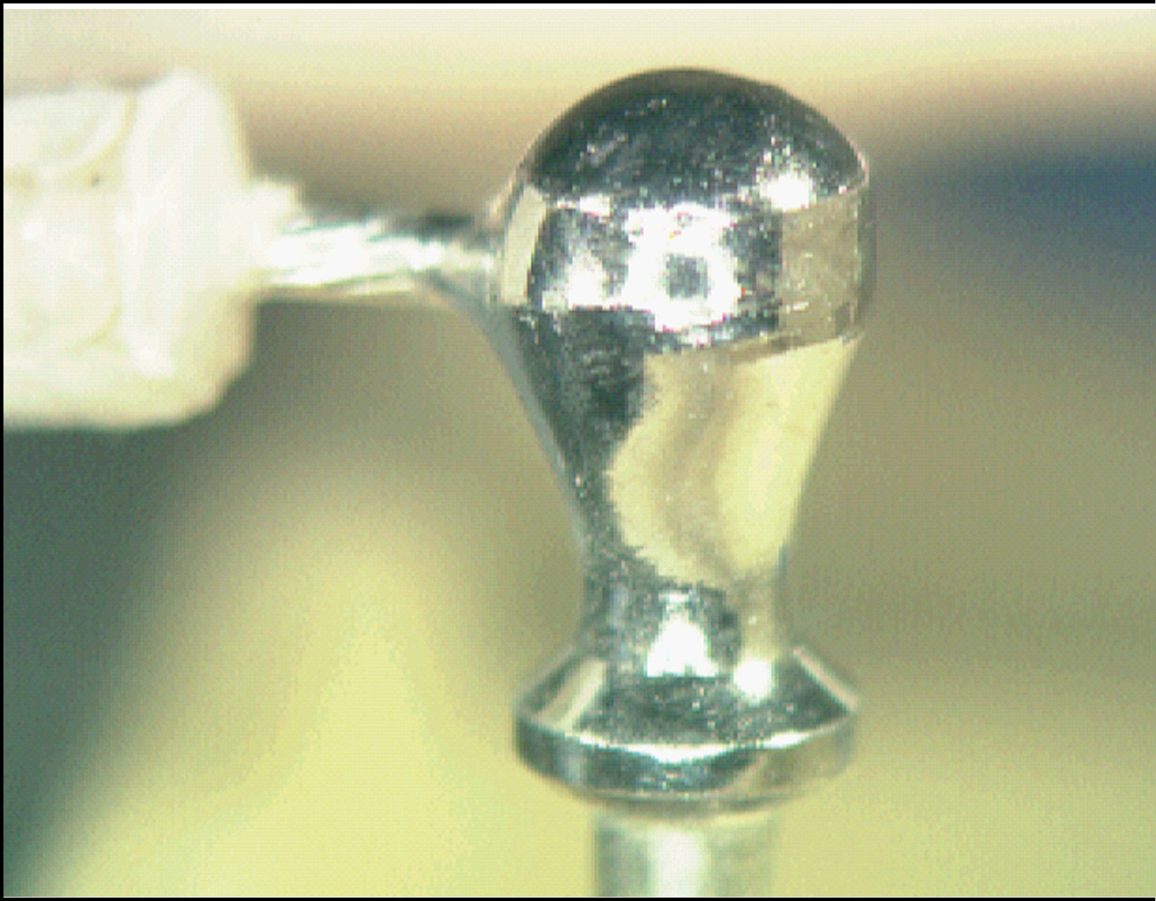 ECSS-Q-ST-70-61_1510702Figure 10-18: High voltage connection
Solderless components
ECSS-Q-ST-70-61_1510703Solderless connection configuration shall be identified in the DCL.
ECSS-Q-ST-70-61_1510704Solderless connection configuration shall be identified during the assembly MPCB.
ECSS-Q-ST-70-61_1510705Acceptance criteria for the assembly shall be proposed by the supplier based on the design and assembly verification results.
It is good practice to perform X Ray inspection.
ECSS-Q-ST-70-61_1510706No overhang shall be permitted.
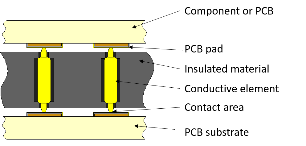 Figure 10-19: Solderless assembly configuration
Post soldering process requirements
Cleaning of PCB assemblies
General
ECSS-Q-ST-70-61_1510707When the solder has solidified and cooled, flux and residue shall be removed using a solvent in accordance with clause 6.4.
ECSS-Q-ST-70-61_1510708Contamination of electrical contact surfaces by the dissolved flux residues shall be prevented.
- 1 Non hermetic components such as connectors, switches and solderless contacts can be degraded by such contamination.
- 2 The protection can be performed using a mask.
- 3 Examples of electrical contact surfaces are those in switches, potentiometers, or connectors.
ECSS-Q-ST-70-61_1510709When insulated wires are on a board, local cleaning shall be performed in such a manner that avoids penetration of solvent under wire insulation and prevents its entry into the interior of components.
ECSS-Q-ST-70-61_1510710Flux and residue shall be removed within a maximum period of 8 hours after soldering operations. - 1 It is good practice to remove flux residues directly after the soldering operation because even rosin fluxes are difficult to remove after longer ageing.
- 2 Longer period can be considered with a successful SIR test presented to Approval Authority.
ECSS-Q-ST-70-61_1510711All fluxes, machine oils and ionisable contaminants on the assembly shall be removed within one hour of the wave soldering operation.
ECSS-Q-ST-70-61_1510712PCB assemblies shall not be immersed in cleaning solvents for more than 30 minutes for each cleaning operation.
Long immersion times can promote galvanic corrosion between adjacent metallic surfaces.
ECSS-Q-ST-70-61_1510713Ultrasonic cleaning shall not be used for PCBs populated with components.
Verification of cleanliness
ECSS-Q-ST-70-61_1510714The verification of the PCB cleanliness shall be performed for the following cases:
- for the first verification programme performed by a company or
- if the conditions of Table 13-1 request it.
Demonstration of cleanliness on a larger package such as AAD can be done by breaking off the package body of one of the verification samples after assembly and cleaning. Inspection is done under magnification to detect any flux residues to replace the SIR test.
ECSS-Q-ST-70-61_1510715The supplier shall demonstrate the cleanliness level for each combination of substrate material type, flux type, soldering process and cleaning process.
ECSS-Q-ST-70-61_1510716The cleanliness verification shall be done for a flight representative production flow.
- 1 A typical production flow can include collective assembly, automatic cleaning machine, manual soldering as well as manual cleaning.
- 2 It is recommended to include extra test samples with a subset of the process flow, for example only collective or only manual soldering with associated cleaning, for failure investigation in case of non-conformances. It is also good practice to include reference bare PCB samples which have only been cleaned and baked.
ECSS-Q-ST-70-61_1510717The effectiveness of the cleaning shall be verified with the following tests: - Sodium chloride (NaCl) equivalent ionic contaminants test in accordance with clause 11.1.4.
- Surface Insulation Resistance (SIR) test in accordance with clause 11.1.3.
On FM boards, the effectiveness of the cleaning can be verified by using a UV lamp from 300 nm - 400 nm range.
Surface Insulation Resistance (SIR) testing
ECSS-Q-ST-70-61_1510718 SIR test shall be implemented at first verification and after any process changes according to Table 13-1 or due to the introduction of components for which cleanliness testing is considered worst case and not covered by previous analysis.
ECSS-Q-ST-70-61_1510719Surface Insulation Resistance (SIR) testing shall be performed in accordance with IPC-TM-650 Test method 2.6.3.7, with the following modifications:
- The test PCBs consist of same PCB material type and surface finish and solder mask, if applicable, as the flight boards.
- The test patterns are as minimum compliant to IPC-B-36.
- The SIR test board pattern is adapted to the product design with test patterns representing the components of finest pitch and components with lowest stand-off to the PCB.
- The SIR test boards is populated for process and product representativity.
- The minimum number of SIR test boards is one.
- The SIR test sample is submitted to a flight representative production flow with regards to all handling, cleaning, baking and soldering operations.
- The test boards are visually inspected in accordance with flight representative procedures.
- The duration of the testing is as a minimum 168 hours,
- The SIR is measured every 20 minutes during the complete duration of the test.
- 1 to item 3: Fine-pitch and low stand-off components are of highest risk in case of electromigration.
- 2 to item 3: For the same component width, longer chips are more difficult to clean. For the same component length, wider chips are more difficult to clean.
- 3 to item 4: Commercial plastic components can be used as long as the pitch and stand-off is representative.
ECSS-Q-ST-70-61_1510720The applied voltage during test may be modified from IPC-TM-650 Test method 2.6.3.7 to be representative of flight hardware.
ECSS-Q-ST-70-61_1510721The acceptance criteria for SIR testing shall be as follows: - the surface insulation resistance exceeds 100 MΩ during the complete testing,
- the conductor spacing is not reduced,
- dendrites are absent,
- No corrosion of the conductors is visible.
Minor discoloration of one pole of the comb pattern conductors is acceptable.
Sodium chloride (NaCl) equivalent ionic contaminants testing
ECSS-Q-ST-70-61_1510722Sodium chloride (NaCl) equivalent ionic contaminants shall be measured as follows:
- Use a solution of 75 % isopropyl alcohol and 25 % deionized water for the sodium chloride (NaCl) equivalent ionic contaminants test.
- Calibrate the equipment using a sodium chloride solution of known quantity and composition.
ECSS-Q-ST-70-61_1510723Testing shall be performed according to the equipment manufacturer’s specification.
ECSS-Q-ST-70-61_1510724The minimum number of test boards for sodium chloride NaCl equivalent ionic contaminants testing shall be one.
ECSS-Q-ST-70-61_1510725The test boards shall be visually inspected in accordance with flight representative procedures.
ECSS-Q-ST-70-61_1510726The cleanliness test values shall be as follows: - Starting resistivity: greater than 20 × 106 cm.
- Ending value: The sodium chloride (NaCl) ionic contaminants equivalence value be less than 0,70 µg/cm2 of PCB surface area.
Monitoring of cleanliness
ECSS-Q-ST-70-61_1510727The effectiveness of the post soldering cleaning process employed for PCB assemblies shall be monitored using a sodium chloride (NaCl) equivalent ionic contaminants test in accordance with clause 11.1.4.
The aim of the monitoring is to demonstrate that the verified cleanliness level is maintained.
ECSS-Q-ST-70-61_1510728Cleanliness monitoring may be omitted for solder assemblies using only pure rosin (ROL0) fluxes as defined in Table 6-2.
ECSS-Q-ST-70-61_1510729For fluxes, other than pure rosin (ROL0), cleanliness testing shall be done in case one or more of the following conditions are met:
- at maximum intervals of six months,
- following a change in flux materials,
- following a change in process parameters,
- following actions affecting cleanability.
Statistical control methods can be used to control continuous solvent cleaning processes.
ECSS-Q-ST-70-61_1510730The supplier shall implement and maintain records of test results.
The records can aid early detection of a trend towards nonconformance.
ECSS-Q-ST-70-61_1510731When a test result is unacceptable, a major NCR shall be issued in accordance with ECSS-Q-ST-10-09.
Staking and bonding
ECSS-Q-ST-70-61_1510732Adhesive shall be selected in conformance with clause 6.11.
ECSS-Q-ST-70-61_1510733Adhesive shall be mixed and cured in accordance with the manufacturer’s recommendations.
ECSS-Q-ST-70-61_1510734The process of mixing and applying the adhesive shall be documented by a written procedure or by configured drawings which define the location of the adhesive, the shape and the spread area.
ECSS-Q-ST-70-61_1510735All PTH components weighing more than 5 g shall be staked.
- 1 Staking and bonding can be applied before or after soldering depending on configuration.
- 2 Staking of heavy components can be omitted when verified.
ECSS-Q-ST-70-61_1510736All SMD weighing more than 5 g should be staked. - 1 This is to minimize shock and vibration loading on the leads.
- 2 The adhesive compound can be applied either before or after soldering in conformance with the supplier’s process identification document.
ECSS-Q-ST-70-61_1510737Staking and bonding shall be performed on clean surfaces.
Some surfaces can be prepared to enhance the adhesion for instance. by mechanical abrasion.
ECSS-Q-ST-70-61_1510738Staking and bonding shall not be performed on fused tin lead unless the tin lead surface is limited to < 25 % by area of the bonding surface and demonstrated by verification as specified in clause 13.
Fused tin lead can be locally removed by wicking, using a copper braid.
ECSS-Q-ST-70-61_1510739The adhesive shall not extend onto the solder footprints.
ECSS-Q-ST-70-61_1510740Spread of staking and bonding material onto surrounding areas may be accepted providing the staking and bonding shape is in accordance with the assembly verification.
ECSS-Q-ST-70-61_1510741The adhesive shall not negate the stress relief of the component or terminations.
Stress relief can be negated if staking is in contact with neighbouring leads
ECSS-Q-ST-70-61_1510742Staking and bonding material shall not be in contact with surrounding components or terminals.
ECSS-Q-ST-70-61_1510743Epoxy staking and bonding material shall not be in contact with glass bodied components.
It is good practice to use a sleeve between glass body and adhesive material.
Conformal coating, potting and underfill
ECSS-Q-ST-70-61_1510744Conformal coating shall be selected in conformance with clause 6.11.
ECSS-Q-ST-70-61_1510745Pottings, underfill and conformal coatings shall not negate stress-relief of component leads or connecting wires.
Underfill can be applied before or after soldering depending on configuration.
ECSS-Q-ST-70-61_1510746Pottings, underfill and conformal coatings shall not have adverse effects upon materials used on the substrate, or components attached thereon.
This is particularly important at low service temperatures.
ECSS-Q-ST-70-61_1510747The conformal coating shall be applied such that any defect identified in clause 12.3 are prevented.
Final inspection
General
ECSS-Q-ST-70-61_1510748Each soldered connection shall be visually inspected.
- 1 Annex F includes examples of acceptable and unacceptable workmanship for SMDs.
- 2 Annex E includes examples of acceptable and unacceptable workmanship for PTHs.
ECSS-Q-ST-70-61_1510749Components and conductors shall not be physically moved prior or during visual inspection.
ECSS-Q-ST-70-61_1510750The substrate, solder joint, components and component position, shall be inspected in accordance with: - clause 10.4 for SMDs,
- clauses 8.2, 9 and 10.2.6 for PTHs,
- clause 10.6 for high-voltage connections,
- clause 10.7 for solderless interconnections. ECSS-Q-ST-70-61_1510751The assembly shall be visually inspected in two steps with the following methodology:
- Visual inspection of the assembly is aided by magnification appropriate to the size of the connections between 4x and 10x.
- Detailed inspection is performed with a minimum magnification 20x.
ECSS-Q-ST-70-61_1510752Additional magnification shall be used to resolve suspected anomalies or defects up to 40x.
ECSS-Q-ST-70-61_1510753X-ray inspection shall be applied when there are hidden solder joints that are not visually accessible.
X-ray rejection criteria are defined in clause 12.4.
Visual acceptance criteria
ECSS-Q-ST-70-61_1510754Acceptance criteria for visual inspection shall be as follows:
- a clean, smooth satin to bright undisturbed solder joint surface,
- solder fillets between conductor and termination areas,
- visible contour of wires and leads such that their presence, direction of bend and termination end can be determined,
- complete wetting as evidenced by a low contact angle between the solder and the joined surfaces,
- acceptable amount and distribution of solder,
- absence of any of the defects specified in clause 12.3,
- stress relief,
- exposed base metal at the ends of cut leads in the soldered connection,
- exposed base metal on sides of tracks and soldering pads on substrate,
- haloing at PCB edge and non-plated holes in accordance with Table 10-45 of ECSS-Q-ST-70-60,
- wire soldered on its entire lap contact.
Illustrations of criteria are given in Annex E and Annex F.
Visual rejection criteria
ECSS-Q-ST-70-61_1510755The following nonconformances shall be cause for rejection:
- charred, burned or melted insulation of components,
- conductor pattern separation from circuit board,
- burns on base materials,
- continuous discolouration between two conductor patterns,
- excessive solder including peaks, icicles and bridging, see Annex E for PTH components,
- contaminated solder joints including flux, lint and extraneous material,
- flux residue, solder splatter, solder balls, or other foreign matter on circuitry, beneath components or on adjacent areas,
- dewetting,
- insufficient solder,
- pits, holes or voids,
- granular or disturbed solder joints,
- fractured or cracked solder connection,
- cut, nicked, gouged or scraped conductors or conductor pattern,
- incorrect conductor length,
- incorrect direction of clinch or lap termination on a PCB,
- damaged conductor pattern,
- soldered joints made directly to gold-plated terminals, unless in compliance with requirement 6.9.2b or 7.6.1b,
- cold solder joints,
- component body embedded within solder fillet,
- open solder joints,
- probe marks present on the soldered joint or on the metallization of chip components caused by electrical testing after assembly,
- glass seal not in compliance to MIL-STD-883 Method 2009.8,
- impaired stress relief,
- measling,
- delamination,
- exposed base metal except criteria specified 12.2a.8,
- cracks detected in glass diodes outside the relevant component procurement standard,
- bent connector pins outside the relevant component procurement specification,
- modified component leads shape after assembly even if still within that defined in procurement standard of the item,
- damage of the lead, component or PCB beyond that defined in the procurement standard of the item,
- reduced insulation between leads down to unacceptable value as per ECSS-Q-ST-70-12 clause 14.3.2,
- degraded insulation material of the connector in contact area,
- bubble or void in the conformal coating or potting that are bridging conductive elements,
- bubble, void or delamination in conformal coating and potting between high voltage conductors,
- lack of conformal coating specified on drawing,
- not specified and continuous adhesive forming a bridge in contact with terminals, component body or solder joints,
- excessive degolding,
- insufficient degolding,
- direct bonding on glass component body with epoxy,
- separation of adhesive from the contact surface,
- separation of conformal coating from the surface,
- presence of cracks in the ceramic of components or cover of component.
- any FOD trapped into or under conformal coating on circuitry, beneath components or on adjacent areas.
- 1 Example to item 4: measling, delamination, halo effect.
- 2 Example to item 20: tombstoning.
- 3 to item 21: it is good practice to include flying probe testing in the flow of verification when flying probe testing is commonly performed on FM, for acceptance of the probe marks.
- 4 to item 24: the minimum insulation distance can be found in ECSS-Q-ST-70-12 for assessment of measling criticality.
- 5 Examples to item 30:
- End cap metallization peeling cracks in component, missing metallization are examples of damage.
- Cracks in ceramics mainly occur in chip capacitors, and leadless component with thermal plane termination.
X-ray rejection criteria
ECSS-Q-ST-70-61_1510756The following non-conformances while performing X-ray inspection, with equipment defined in clause 5.5.19, shall be cause for rejection:
- bridges and other unintended metallic materials,
- poor or no wetting of the solder,
- cumulative voids greater than 25 % by area of the solder joint,
- cumulative voids greater than the maximum allowed for specific applications,
- a single void which traverses either length or width of the terminal and exceed 10 % of the total area.
- 1 to item 11: Solder balls are a typical example of unintended metallic material.
- 2 to item 2: It can be difficult to assess the wetting in X-ray, but solder joints with deviating shape or amount compared to the neighbouring connections indicate that a closer look is needed.
- 3 to item 3: The amount of voids can be manually estimated from an X-ray image, without exact quantification by image processing.
- 4 to item 4: Specific applications can be RF, thermal dissipation or electrical grounding. The minimum coverage requirement might need adaptation for these cases based on the specific design.
- 5 to item 4: The amount of voids is highly depending on the PCB footprint design, quality of surface finishes on both PCB and component, as well as the soldering process including solder paste.
- 6 Manual soldering, especially with artificial stand-off can make it difficult to fulfil maximum side overhand and minimum termination contact lengths.
ECSS-Q-ST-70-61_1510757For area array components the criteria and dimensions outside the limits given in Table 10-14 shall be met in addition to the requirements of 12.4a.
ECSS-Q-ST-70-61_1510758Any deviation to requirement 12.4a.3 shall be demonstrated by verification in compliance with requirements from clause 13 and accepted by Approval Authority.
ECSS-Q-ST-70-61_1510759The maximum dose during X-ray inspection shall be less than 5 % of the eligible dose of the most sensitive component according to its specification.
Warp and twist of populated boards
ECSS-Q-ST-70-61_1510760The PCB assembly shall be supported during handling and transportation in order to avoid any mechanical stress on the assembly or component damage.
Mechanical support can be provided by spacer or frame.
ECSS-Q-ST-70-61_1510761The PCB shall not be forced during any operation to compensate warp and twist.
Shims or spacers can be used to accommodate warp and twist during integration.
Inspection records
ECSS-Q-ST-70-61_1510762The result of the final inspection shall be recorded in the manufacturing traveller.
ECSS-Q-ST-70-61_1510763For wave soldering process, a soldering log as specified in clause 13.2.4 shall be put in place.
Verification procedure
Verification approval procedure
Request for verification
ECSS-Q-ST-70-61_1510764The supplier shall provide the following items to the Approval Authority:
- A letter from the supplier signed by the contact person and the quality assurance organization of the supplier describing his experience in assembly and making the request for verification.
- A verification programme in compliance with clause 13.1.4.
- 1 (one) technology sample in compliance with clause 13.1.2. ECSS-Q-ST-70-61_1510765In the frame of a project, the supplier shall provide a RFA Part1 (Request for Approval).
Technology sample
Description of technology sample
ECSS-Q-ST-70-61_1510766Technology sample shall be made when introducing a new assembly process or new supplier.
ECSS-Q-ST-70-61_1510767The supplier shall provide 1 (one) technology sample of flight representative board showing the Flight assembly process capability with components of typical complexity and illustrated in space quality workmanship standards.
Examples of solder joints quality according to space industry are presented in Annex F and Annex E.
ECSS-Q-ST-70-61_1510768Technology sample shall include areas with and without conformal coating if used.
ECSS-Q-ST-70-61_1510769The supplier shall provide a listing of the assembly procedures.
ECSS-Q-ST-70-61_1510770Approval Authority may waive the needs of technology sample.
Evaluation of technology sample
ECSS-Q-ST-70-61_1510771The technology sample shall be assessed by Approval Authority or by a test house recognized by Approval Authority.
ECSS-Q-ST-70-61_1510772The assessment of the technology sample shall include visual inspection report.
ECSS-Q-ST-70-61_1510773Approval Authority may request microsectioning.
ECSS-Q-ST-70-61_1510774Approval Authority shall inform the supplier on the result of inspection of the technology sample.
ECSS-Q-ST-70-61_1510775After examination, the technology sample examination report shall be sent to the supplier.
ECSS-Q-ST-70-61_1510776Approval Authority shall inform the supplier on acceptance regarding the start of the next stages of the approval process.
Audit of assembly processing
ECSS-Q-ST-70-61_1510777Provided the technology sample specified in 13.1.2 is acceptable, Approval Authority shall audit the assembly facility at a time when the assembly line is in operation.
ECSS-Q-ST-70-61_1510778The findings of the audit shall remain confidential between Approval Authority and the supplier.
ECSS-Q-ST-70-61_1510779The audit of the supplier’s assembly line shall be performed prior to the start of a verification programme.
ECSS-Q-ST-70-61_1510780The Approval Authority shall submit to the supplier a copy of the audit report.
- 1 The assembly line audit report is a customer document provided to the supplier and is used as input for the customer to decide if the verification programme can be further implemented.
- 2 An example of audit report template is given in Annex G.
ECSS-Q-ST-70-61_1510781The audit shall also include a further onsite review of the documentation listed in Annex A.2.1.
ECSS-Q-ST-70-61_1510782Assembly line audit shall be conducted every four years by Approval Authority or after any major changes in the manufacturing floor such as new equipment.
Verification programme documentation
ECSS-Q-ST-70-61_1510783A verification programme shall be submitted to the Approval Authority for acceptance prior to the start of assembly verification in accordance with DRD from Annex A.
Requirement A.2.1b gives possibility to tailor verification programme.
ECSS-Q-ST-70-61_1510784Verification programme shall be in compliance with:
- clause 13.2 for generic verifications,
- clause 13.3 for ceramic area array components,
- clause 13.4 for assembly verification with electrical testing procedure,
- clause 13.5 for verification with reduced temperature range,
- clause 13.6 for solderless process.
ECSS-Q-ST-70-61_1510785The schedule of the verification activities shall be provided and updated.
ECSS-Q-ST-70-61_1510786Any nonconformance or major change with reference to the verification plan shall be notified to the Approval Authority within one week.
Verification samples and testing
ECSS-Q-ST-70-61_1510787The PCB material, PCB build-up, interconnections and footprint used for the verification shall be representative of the FM hardware.
ECSS-Q-ST-70-61_1510788Assembled components shall be flight representative with regards to construction, materials and lead finish.
ECSS-Q-ST-70-61_1510789Assembly shall be flight representative including mechanical and thermal configuration.
ECSS-Q-ST-70-61_1510790Surface mount connectors not screwed to the PCB shall be verified in the flight representative configuration.
ECSS-Q-ST-70-61_1510791For surface mount connectors not screwed to the PCB, mating/demating operations, interconnections to other boards and harnesses shall be included in the verification for flight representativity.
ECSS-Q-ST-70-61_1510792For assembly sensitive components, where the failure mode is damage of the component QM grade level components should be used as a minimum.
The ESA list of assembly sensitive components is regularly updated and published on ESCIES for information, see www.escies.org, Technologies - ESA SMT Verification. ESA-MPSMO-018961.
ECSS-Q-ST-70-61_1510793The components used for the verification shall be listed in the Verification programme documentation, in accordance with the DRD in Annex A.
It is the responsibility of the company that the soldering method and temperature are compliant with the manufacturer datasheet or technical notes.
ECSS-Q-ST-70-61_1510794Only component types used during the verification programme shall be regarded as approved.
- 1 Approved components are listed in the assembly summary table.
- 2 Component approved by similarity, as per clause 13.8, are not listed in the Assembly Summary Table
ECSS-Q-ST-70-61_1510795The verification samples shall be assembled and tested according to agreed verification programme.
ECSS-Q-ST-70-61_1510796All test conditions shall be compliant with requirements from clause 14.
Final verification review
ECSS-Q-ST-70-61_1510797The verification report shall be in compliance with DRD from Annex B.
ECSS-Q-ST-70-61_1510798The verification report shall be made available to the Approval Authority.
ECSS-Q-ST-70-61_1510799The supplier shall organise with the Approval Authority a final verification review.
The assembly processes can be reviewed during the meeting to issue the PID. Verification of closure of the actions identified during the audit of the manufacturing line.
Approval status of assembly line
ECSS-Q-ST-70-61_1510800Following the completion of the final verification review, the following documents shall be submitted to the Approval Authority:
- PID
- Assembly summary tables.
ECSS-Q-ST-70-61_1510801The assembly summary tables shall be prepared by the supplier according to DRD from Annex D.
ECSS-Q-ST-70-61_1510802In case of changes in assembly line impacting its approval, an audit shall be conducted to re-establish the approval as specified in clause 13.1.3.
A non-exhaustive list of changes that impact the Approval of the line is given in Table 13-1.
ECSS-Q-ST-70-61_1510803A letter confirming the completion of a successful verification programme shall be sent to the contact person of the supplier from the Approval Authority, with the Assembly summary table in conformance with the DRD of Annex D.
- 1 The letter and the Assembly summary table provide evidence of the verification approval to a third party.
- 2 The approval of verification applies to all space projects from the date of the approval until withdrawal.
ECSS-Q-ST-70-61_1510804Reference to the Assembly summary table number shall be made on each Space project declared processes list.
ECSS-Q-ST-70-61_1510805Assembly verification status of the electronic hardware shall be reviewed during assembly MPCB review.
A guideline to support MPCB review is: ESA-TECQTM-MO-1931 Issue 3 “Guideline for the review of Approval status of electronics assembly configurations during MPCB”.
ECSS-Q-ST-70-61_1510806Except for components covered by requirement 13.1.7j, verification may be omitted for components for which supplier can demonstrate their acceptance through previous verification heritage, listed in their approved summary table.
ECSS-Q-ST-70-61_1510807Assembly sensitive components that have successfully passed the assembly verification in compliance with this standard, and are outside of what is defined in 3.2.2,shall not be considered as assembly sensitive component in the supplier PID.
ECSS-Q-ST-70-61_1510808The supplier shall maintain a list of assembly sensitive components.
ECSS-Q-ST-70-61_1510809Assembly sensitive components listed in the supplier PID shall be submitted to re-verification every four years to monitor the stability of the assembly.
ECSS-Q-ST-70-61_1510810The re-verification of assembly sensitive components specified in the requirement 13.1.7j may be performed on limited verification programme with worst case configuration identified during initial verification provided acceptance of Approval Authority.
- 1 One substrate, one package per component type, three samples per component.
- 2 For leadless components, mechanical testing can be omitted.
- 3 Non-destructive characterization can be proposed as alternative to microsection.
Withdrawal of approval status
ECSS-Q-ST-70-61_1510811The approval status of the supplier shall be withdrawn if any of the following occurs:
- Repetitive supply problems and manufacturing defects,
- Undeclared changes of items listed in Table 13-1,
- Numerous non compliances to the PID.
- 1 Renewed approval can be granted following a review of the discrepancies.
- 2 A repeat, or partial repeat of the verification programme can be requested by the Approval Authority.
Verification programme
General
ECSS-Q-ST-70-61_1510812The approval of mounting and supporting of components, terminals and conductors, as specified in this standard, shall be applicable only to assemblies designed to continuously operate over the mission within the temperature limits of -55 C to +85 C at solder joint level.
ECSS-Q-ST-70-61_1510813Compliance to environmental range within -55 °C to +85 °C at solder joint level for the mission shall be stated.
ECSS-Q-ST-70-61_1510814The supplier shall demonstrate verification for each combination of substrate material type, PCB footprint, component type, soldering technique applied, staking and bonding, lead forming configuration, solder mask and conformal coating as used on FM.
- 1 Material type groups as defined in Table 6-1 of ECSS-Q-ST-70-12.
- 2 Vapour phase reflow, convection reflow, hot air and hand soldering are examples of different soldering techniques.
ECSS-Q-ST-70-61_1510815Verification of area array components shall be performed in accordance with the requirements in clause 13.3.
ECSS-Q-ST-70-61_1510816Except for area array components which are covered by clause 13.3, verification may be performed with electrical testing procedure in compliance with clause 13.4.
ECSS-Q-ST-70-61_1510817Verification of solderless assemblies shall be performed in compliance with clause 13.6.
ECSS-Q-ST-70-61_1510818Verification programme with reduced temperature range in accordance with clause 13.5 may be applied to reduce risk of failure during thermal cycling due to CTE mismatch between component and PCB. - 1 Ceramic chip capacitors type II are highly prone to cracks in the ceramic. It has been demonstrated that the type of cracks and length of cracks seen in microsectioning at the top side are directly correlated to the temperature range during thermal cycling as well as the temperature gradient. It is therefore for this type of components recommended to perform verification programme with reduced temperature range from the beginning, not only after a previously failed verification programme.
- 2 For chip capacitors it is good practice to perform the verification on the capacitance value used which has the thinnest cover plate and most densely packed dielectric planes. Cover plate is the distance between external surface. and first electrode.
ECSS-Q-ST-70-61_1510819The verification shall be performed on at least 3 (three) components except for the assembly of sensitive components where 5 (five) components are used per configuration in the verification programme.
ECSS-Q-ST-70-61_1510820When assembly sensitive component is listed in summary table, if the verification was performed with less than 5 (five) components, a new verification shall be performed.
ECSS-Q-ST-70-61_1510821Verification of the assembly shall be performed with a nominal process and a repair process for each component.
Manual process covers a range of processes such as hand soldering, hot gas station and IR station.
ECSS-Q-ST-70-61_1510822The nominal process shall be representative of the FM manufacturing flow.
If both collective and non-collective processes are used on FM, verification board is submitted to both processes also in verification.
ECSS-Q-ST-70-61_1510823No rework shall be performed before MIP1 except for manually soldered components.
ECSS-Q-ST-70-61_1510824Rework of components, other than manually soldered, shall be decided during the MIP1
ECSS-Q-ST-70-61_1510825For chip components, more than 20 % of reworked soldered joints per component type and assembly configuration shall not be acceptable.
ECSS-Q-ST-70-61_1510826For all components except those defined in requirement 13.2.1n, more than 10 % of reworked soldered joints per component type and assembly configuration shall not be acceptable.
ECSS-Q-ST-70-61_1510827Reworks outside of what is allowed in 13.2.1m and 13.2.1n may be accepted by Approval Authority.
Some packages due to their complexity can be more difficult to assemble without any rework.
ECSS-Q-ST-70-61_1510828Any repair or modification, not compliant to ECSS-Q-ST-70-28, shall be submitted to a verification programme as agreed with the Approval Authority.
ECSS-Q-ST-70-61_1510829The supplier’s repair process using the nominal manual process including removing and replacing of 1 (one) of each type of mounted component shall be submitted to verification testing with the exception of AAD assembly verification for which a minimum of 2 (two) parts are being repaired.
The supplier has the option to perform more than 1 (one) repair for each type of component.
ECSS-Q-ST-70-61_1510830For each type of component, per configuration, the repair shall be performed on the largest component.
ECSS-Q-ST-70-61_1510831For repair verification of collective assembled components, the repair shall be performed only on the components being assembled by manual soldering method, provided the same assembly configuration.
The repair is required on the hand soldering process to keep a sample of 3 (three) or 5 (five) on the collective assembly configuration.
ECSS-Q-ST-70-61_1510832Verification testing of commercial components shall be performed for each lot in conformance with this clause 13.2.1, except when requirement 13.8.1d can be met.
ECSS-Q-ST-70-61_1510833Terminations to be microsectioned shall be connected to the internal PCB layers.
The terminations to be microsectioned are described in Table 14-5.
ECSS-Q-ST-70-61_1510834The verification sample shall be submitted to 2 (two) nominal soldering method reflows when reflow is performed on both PCB sides of the FM.
The supplier has the option to flip the board for the second reflow.
ECSS-Q-ST-70-61_1510835The verification programme shall be performed in accordance with Figure 13-1.
ECSS-Q-ST-70-61_1510836A soldering log as specified in clause 13.2.4 shall be put in place for all soldering processes involved in a board manufacturing during verification programme.
ECSS-Q-ST-70-61_1510837The soldering log shall be made available to the Approval Authority.
ECSS-Q-ST-70-61_1510838The conditions associated with long term storage, extensive ground testing, mechanical stress after launch, high temperature application with or without thermal cycles shall be assessed by the supplier.
ECSS-Q-ST-70-61_1510839The environmental conditions of the mission including ground testing shall be covered by the environmental conditions of the verification programme.
ECSS-Q-ST-70-61_1510840For surface mounted components the total number of temperature cycles shall be 500, except for the cases defined in requirement 13.3.3g and requirement 13.4p.
ECSS-Q-ST-70-61_1510841For components mounted in plated through holes the total number of temperature cycles shall be 200.
ECSS-Q-ST-70-61_1510842When mechanical bonding is underneath the component, microsectioning of one component may be performed after vibration and 50 thermal cycles to justify the integrity of the bonding.
The component can be 1 (one), not the one repaired, of the 3 (three) assembled components which were cut out from the same verification board after the 50 thermal cycles.
ECSS-Q-ST-70-61_1510843Prior to start verification assembly the supplier shall organize a MRR with two weeks notification with the Approval Authority
- 1 The PCB design is reviewed to check compliance with requirements from clause 13.1.5.
- 2 During the review, the Approval Authority can check that the verification programme is approved by all parties and that all actions are closed.
ECSS-Q-ST-70-61_1510844The supplier shall organise a MIP1 with two weeks notification, with the Approval Authority prior to any conformal coating.
The Approval Authority can delegate the MIP1 to the supplier.
ECSS-Q-ST-70-61_1510845Prior to any environmental testing, the supplier shall organise with the Approval Authority a TRR with two weeks notification during which the MIP1 outputs and outstanding actions are reviewed.
The Approval Authority can delegate the action review to the supplier.
ECSS-Q-ST-70-61_1510846The supplier shall organise with Approval Authority a MIP2 with two weeks notification at the completion of the environmental test.
The Approval Authority can delegate the MIP2 to the supplier.
ECSS-Q-ST-70-61_1510847The supplier shall organize with the Approval Authority a final VR during which the environmental tests results are reviewed.
 ECSS-Q-ST-70-61_1510848Figure 13-1 : Generic soldering verification flow
Verification for PTH manual soldering
ECSS-Q-ST-70-61_1510849Any soldering configuration not covered by requirements from clauses 8.2, 9,10.2.6 and 10.3 or covered but for which assembly verification is requested shall be verified in accordance with clause 13.2.1.
ECSS-Q-ST-70-61_1510850A process specific verification programme shall be performed for through hole component assemblies with stress relief that are not compliant to clause 8.2.
Additional verification for wave soldering
ECSS-Q-ST-70-61_1510851For components that are not assembly sensitive, the supplier shall provide 2 (two) assembled PCBs with at least 3 (three) components of each type per board and 1 (one) non-assembled PCB as reference.
ECSS-Q-ST-70-61_1510852For assembly sensitive components, the supplier shall provide 2 (two) assembled PCBs with at least five components of each type per board and 1 (one) non-assembled PCB as reference.
ECSS-Q-ST-70-61_1510853Each board shall have an identical layout and be from the same batch.
ECSS-Q-ST-70-61_1510854The layout and component density shall be similar to that envisaged for FM boards.
ECSS-Q-ST-70-61_1510855Warp and twist of all assembled PCBs shall be measured for wave soldering verification, according to clause 14.5.
ECSS-Q-ST-70-61_1510856Electrical continuity measurements shall be performed on wave soldered multilayer PCBs according to clause 14.7.
ECSS-Q-ST-70-61_1510857One component of each type per board shall be submitted to repair.
ECSS-Q-ST-70-61_1510858More than 5 % of reworked soldered joints per component shall not be accepted.
Soldering log
ECSS-Q-ST-70-61_1510859The soldering log shall contain as a minimum the following data:
- Board identification
- Board technology description: materials, build up, ground planes
- Soldering process identification
- Main parameters for the soldering process
- List of identified defects
- Number of reworks performed on each solder joint
- Calculation of percentage of defects
- Inspectors observations
- Any miscellaneous remark of interest.
An example of a soldering log for a wave process soldering is given in Figure 13-2.
|
Part identification Wave soldering parametersAssembly: __________ PCB P/N: __________ Preheat temp: ________ Solder temp: ________ Conveyor Speed: ________ Wave height: _________
| |||||||||||||||||||
|
Description
|
Insufficient
|
Excess
|
Miscellaneous
|
|
|||||||||||||||
|
MLB No. of through holes: ______ No. of layers: ______Ground plane estimated area: Topside: ______% Botside: ______%
|
T: component side; B: bottom side
|
Lead poor wetting
|
Pad poor wetting
|
Large voids
|
Small bottomless voids
|
Insufficient solder flow-thru
|
Depressed solder
|
Bridging
|
Icicling
|
Accumulations
|
Excess solder (lead obscured)
|
Stress-relief bends filled
|
Raised component
|
|
|||||
|
Acceptable rework level: ___% total
|
Date
|
Inspector
|
Insptn. S/N
|
Other solder discrepancies (specify)
|
Subtotals
|
% for rework
| |||||||||||||
|
Inspector’s observations:
|
|
|
|
T
|
|
|
|
|
|
|
|
|
|
|
|
|
|
|
|
|
B
|
|
|
|
|
|
|
|
|
|
|
|
|
|
||||||
|
|
|
|
T
|
|
|
|
|
|
|
|
|
|
|
|
|
|
|
|
|
|
B
|
|
|
|
|
|
|
|
|
|
|
|
|
|
||||||
|
Totals:
| |||||||||||||||||||
Figure 13-2: Example of soldering log for joints discrepancy log
Special verification testing for ceramic area array components
General
ECSS-Q-ST-70-61_1510860The assembly verification of ceramic AADs shall be divided in the following 2 (two) steps, as shown in Figure 13-3.
- Demonstration of capability in accordance with clause 13.3.2, and
- Demonstration of electrical integrity in accordance with clause 13.3.3.
- 1 Once the capability samples show a satisfactory result the verification of AAD can commence.
- 2 Capability samples can be excluded from the programme if the supplier can demonstrate previous verification heritage.
ECSS-Q-ST-70-61_1510861The capability and verification samples shall be representative of the FM hardware.
For example, PCB build-up and size, mechanical fixation, component packages.
It is recommended to have a successful IST test on PCB to avoid failing the assembly verification due to damaged PCB.
ECSS-Q-ST-70-61_1510862The PCB material, footprint, via technology used for the capability and verification samples shall be the same and interconnection similar as the ones used for the FM hardware.
HDI, blind via and buried via are different types of via technologies.
ECSS-Q-ST-70-61_1510863The verification shall be performed with daisy chain components to demonstrate a reliable electrical function of the PCB and the package interface throughout the environmental test campaign.
 ECSS-Q-ST-70-61_1510864Figure 13-3: Area Array component verification programme flow chart
Evaluation of AAD capability samples
ECSS-Q-ST-70-61_1510865The supplier shall manufacture and demonstrate that the 2 (two) capability samples are in conformance with the requirement 13.3.2i before the manufacture of the verification samples using daisy chain components can be initiated.
ECSS-Q-ST-70-61_15108662 (two) components shall be assembled with the nominal reflow process.
The supplier can use daisy chain packages for the capability to have an early results of electrical monitoring during thermal cycles.
ECSS-Q-ST-70-61_1510867One of the components from requirement 13.3.2b shall be removed and replaced with a new component using the repair process.
ECSS-Q-ST-70-61_1510868When nominal and repair processes are identical then the number of components, may be reduced to 1 (one) which is repaired
The total number of components needed is 2 (two).
ECSS-Q-ST-70-61_1510869The components shall be inspected in conformance with requirements from the clause 10.4.14.
ECSS-Q-ST-70-61_1510870The components shall be submitted to vibration testing in conformance with requirements from the clause 14.7.
ECSS-Q-ST-70-61_1510871The components shall be submitted to shock testing in conformance with clause 14.9.
ECSS-Q-ST-70-61_1510872The components shall be submitted to 500 thermal cycles in conformance with requirements from the clause 14.11.
ECSS-Q-ST-70-61_1510873After environmental tests completion, microsectioning of the components shall be performed to demonstrate PCB integrity in the AAD area with respect to:
- Damage to the component outside the procurement specification,
- Damages outside of what is allowed in clause 14.15.3.
- Damages outside of what is allowed in clause 14.16.
The purpose of the capability samples is to show that the PCB and the component body are intact after the assembly and repair of AAD and environmental testing (vibration, mechanical shock and 500 temperature cycles). A crack in the columns or balls is not considered as reason for rejection.
Electrical verification of AAD assembly
ECSS-Q-ST-70-61_15108745 (five) components shall be assembled for each nominal assembly method and mounting configuration.
ECSS-Q-ST-70-61_15108752 (two) of the assembled components shall be removed and replaced with new components using the repair process.
ECSS-Q-ST-70-61_1510876When nominal and repair processes are identical then the number of components, may be reduced to 3 (three) out of which 2 (two) are repaired.
The total number of components needed is 5 (five).
ECSS-Q-ST-70-61_1510877The components shall be inspected in conformance with requirements from the clause 10.4.14.
ECSS-Q-ST-70-61_1510878The 5 (five) components shall be submitted to vibration testing in conformance with requirements from the clause 14.7.
ECSS-Q-ST-70-61_1510879The 5 (five) components shall be submitted to shock testing in conformance with requirements in clause 14.9.
ECSS-Q-ST-70-61_1510880The 5 (five) components shall be submitted to 1500 thermal cycles with temperature conditions in conformance with clause 14.11 and with continuous electrical monitoring in accordance with clause 14.6.
ECSS-Q-ST-70-61_1510881Resistance measurement shall be done, at ambient, before and after any mechanical testing in accordance with clause 14.6.
ECSS-Q-ST-70-61_1510882After environmental testing the verification samples shall fulfil the acceptance criteria in accordance with clause 14.16.
Assembly verification with electrical testing procedure
ECSS-Q-ST-70-61_1510883Except for the cases specified in requirement 13.4b the supplier may propose assembly verification with electrical testing procedure as an alternative method.
ECSS-Q-ST-70-61_1510884Leadless chip capacitors and leadless components with plane termination shall not be assembly verified through electrical testing procedure.
Capacitor and TO276 packages such as SMD05, SMD1, SMD2 and SMD5C, are excluded as the failure mechanism is crack in ceramic.
ECSS-Q-ST-70-61_1510885Assembly verification with electrical testing procedure shall be performed in accordance with Figure 13-4 with samples for both capability verification with microsectioning and with electrical verification.
ECSS-Q-ST-70-61_1510886Verification of capability shall be performed on at least one component except for the assembly sensitive components where 5 (five) components are assembled with nominal process.
ECSS-Q-ST-70-61_1510887One of the components from requirement 13.4d shall be removed and replaced with a new component using the repair process providing the repair process is identical to the nominal assembly.
ECSS-Q-ST-70-61_1510888If the repair procedure is different from the nominal assembly, a separate assembly verification with full number of capability as well as electrical verification samples shall be performed.
ECSS-Q-ST-70-61_1510889Capability samples may be excluded from the programme if capability can be demonstrated through previous verification heritage.
ECSS-Q-ST-70-61_1510890Verification with electrical monitoring shall be performed on at least 32 components assembled for each assembly configuration with nominal process.
- 1 Machine reflow, hand soldering are the examples of assembly method.
- 2 The assembly of the capability and the electrical verification samples can be made on the same board.
ECSS-Q-ST-70-61_1510891One of the components from requirement 13.4h, except for assembly sensitive components where it is 5 (five) components, shall be removed and replaced with new components using the repair process.
ECSS-Q-ST-70-61_1510892All solder terminations shall be continuously electrically monitored throughout the temperature cycling
ECSS-Q-ST-70-61_1510893The electrical value of components for electrical monitoring shall be selected to be able to detect anomalies in the solder joint: - for resistor zero ohm or the lowest value in the procurement specification,
- for other types, custom daisy chain. ECSS-Q-ST-70-61_1510894In case of non-representative daisy chain component to FM one, the use of functional component may be proposed providing agreement of Approval Authority.
Example of such components are commercial components.
ECSS-Q-ST-70-61_1510895For the capability samples microsectioning shall be performed in accordance with clause 14.14 after verification steps in accordance with Figure 13-1.
ECSS-Q-ST-70-61_1510896If capability and electrical monitoring samples are on the same board they shall be separated before the microsectioning of the capability samples and before the environmental tests for the samples for electrical monitoring.
ECSS-Q-ST-70-61_1510897The samples for electrical monitoring shall be submitted to vibration testing in conformance with requirements from clause 14.8 and shock testing in conformance with requirements in clause 14.9.
ECSS-Q-ST-70-61_1510898The samples for electrical monitoring shall be submitted to 1500 thermal cycles in conformance with requirements in clause 14.11 and with continuous electrical monitoring in accordance with clause 14.6.
ECSS-Q-ST-70-61_1510899Any failed component shall be subjected to failure analysis.
ECSS-Q-ST-70-61_1510900If the first failure occurs before the end of the 1500 thermal cycles, the number of cycles before the first failure shall be identified as the component assembly verification limitation.
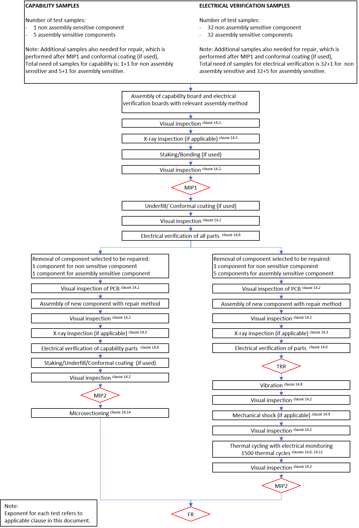 ECSS-Q-ST-70-61_1510901Figure 13-4: Assembly verification with electrical testing procedure
Verification programme with reduced temperature range
ECSS-Q-ST-70-61_1510902Verification programme with reduced temperature range may be applied to reduce risk of failure during thermal cycling due to CTE mismatch between component and PCB.
- 1 The majority of assembly sensitive components (see definition 3.2.2) has CTE mismatch between components and PCB as root cause of failure. Reduction of the temperature range and the temperature gradient can lower the risk of failure due to such root cause, but the thermal cycling will take a longer time. A case-by-case trade-off based on risk vs leadtime is necessary.
- 2 Ceramic chip capacitors type II are highly prone to cracks in the ceramic. It has been demonstrated that the type of cracks and length of cracks seen in microsectioning at the top side are directly correlated to the temperature range during thermal cycling as well as the temperature gradient. It is therefore for this type of components recommended to perform verification programme with reduced temperature range from the beginning, not only after a previously failed verification programme.
- 3 For ceramic chip capacitors it is good practice to perform the verification on the capacitance value used which has the thinnest cover plate and most densely packed dielectric planes.
- 4 It is good practice to apply verification with reduced temperature range for leadless components with plane termination such as SMD0.5 to reduce the risk of cracks in the ceramic.
ECSS-Q-ST-70-61_1510903Verification programme with reduced temperature range shall follow the generic flow described in Figure 13-1, except for the temperature cycling conditions that are modified in compliance with clause 14.12.
ECSS-Q-ST-70-61_1510904Components that have passed a successful verification with reduced temperature range in compliance with this clause may be added in the assembly summary tables as tailored verification, provided approval by the Approval Authority.
ECSS-Q-ST-70-61_1510905Request for approval shall be submitted in each project where the component with tailored verification is used to justify that the verified temperature range covers the mission in which it is intended to be used.
Verification for solderless process
ECSS-Q-ST-70-61_1510906The verification of solderless process shall be performed on flight representative assembly configuration in accordance with Figure 13-5.
Representative assembly configuration includes elements for thermal dissipation configuration.
ECSS-Q-ST-70-61_1510907The verification tests shall be performed to show absence of degradation within the solderless interconnection part, PCB and component during all ground and in-orbit mission.
Possible degradations can be creeping of the spring, fretting degradation of the contact.
ECSS-Q-ST-70-61_15109086 (six) components shall be assembled with the same mechanical configuration as flight model.
ECSS-Q-ST-70-61_1510909Mate/demate number shall permit to cover the application requirement with a margin of 4 in compliance with Table 4-4 of ECSS-E-ST-33-01.
ECSS-Q-ST-70-61_1510910Minimum vibration levels shall be in compliance with requirement 14.8e.
ECSS-Q-ST-70-61_1510911Shock test shall be performed in conformance with requirements from clause 14.9.
ECSS-Q-ST-70-61_1510912Electrical monitoring shall be carried out according to clause 14.6 before and after mate/demate, and during vibration and shock tests, if the equipment is to be functional during launching phases.
ECSS-Q-ST-70-61_1510913The samples for environmental testing shall be submitted to 500 thermal cycles with temperature conditions in conformance with clause 14.11 and with continuous electrical monitoring in accordance with clause 14.6.
ECSS-Q-ST-70-61_1510914Damp heat test shall be performed for all applications in compliance with clause 14.10.
ECSS-Q-ST-70-61_1510915In case of long-term storage application, project specific requirements may apply instead of requirement 13.6i.
ECSS-Q-ST-70-61_1510916Electrical continuity test according to clause 14.6 shall be performed to verify absence of degradation of the connection after damp heat test.
ECSS-Q-ST-70-61_1510917Life test shall be performed in accordance with clause 14.13 and with continuous electrical monitoring in accordance with clause 14.6 to evaluate the spring reliability.
ECSS-Q-ST-70-61_1510918Life test may be omitted provided representative test were performed by the component manufacturer.
ECSS-Q-ST-70-61_1510919Visual inspection criteria in compliance with clause 12 shall apply to interposer, component and PCB.
ECSS-Q-ST-70-61_1510920Microsections of interposer, component and PCB shall be done according to clause 14.15 in order to verify absence of plating damage at interposer level, component damage and laminate cracks or plating damage in the PCB.
Microsectioning can be performed after dismounting of the assembly.
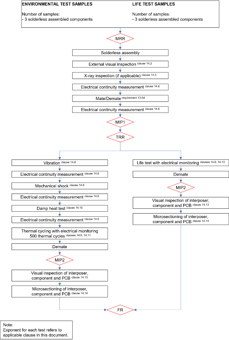 ECSS-Q-ST-70-61_1510921Figure 13-5: Verification procedure for solderless technology
Conditions for delta verification
ECSS-Q-ST-70-61_1510922The supplier shall undertake a verification for any new configuration not covered by similarity rules in accordance with requirements from clause 13.8.
ECSS-Q-ST-70-61_1510923The delta verification shall be performed when changes are undertaken as specified in Table 13-1.
ECSS-Q-ST-70-61_1510924For a process delta verification program, the number of samples may be tailored from the general requirements from clause 13.2, depending on the type of process changes made, subject to approval by the Approval Authority.
- 1 The selection criteria are based on worst cases depending on the change of process to be verified.
- 2 For PCB materials change, examples of worst cases are CTE mismatch, thermal dissipation, stiffness, glass transition temperature and copper peel strength.
ECSS-Q-ST-70-61_1510925For delta verification associated with process change the verification boards shall be designed such that they are representative of the new process.
ECSS-Q-ST-70-61_1510926A delta-verification programme in accordance with the DRD from Annex A shall be submitted for approval to the Approval Authority.
ECSS-Q-ST-70-61_1510927Table 13-1: Conditions invoking verification
|
Examples of changes
|
Cleanliness and solvent compatibility tests
|
Limited verification without environmental tests
|
Full verification with environmental tests
|
|
New component mounting configuration
|
|
|
X
|
|
New component size not covered by conditions for similarity
|
|
|
X
|
|
New PCB material type
|
|
|
X
|
|
New PCB surface finish
|
|
|
X
|
|
New solder paste without change of alloy, powder size distribution or flux activation type
|
X
|
X
|
|
|
New solder paste with new alloy, flux activation type and/or different physical and chemical characteristics
|
X
|
|
X
|
|
New flux activation type for manual soldering
|
X
|
X
|
|
|
New cleaning solvent or cleaning process
|
X
|
|
|
|
New reflow profile 1
|
|
|
X
|
|
New solder paste deposition, or reflow equipment without process change
|
|
X
|
|
|
New component placing equipment of same process method
|
|
X
|
|
|
New solder paste depositing process
|
|
|
X
|
|
New reflow equipment with process change
|
|
|
X
|
|
New conformal coating application process or equipment(without material or thickness change)
|
|
X
|
|
|
Move of manufacturing location outside the clean room specified in the PID
|
|
X
|
|
|
1 The reflow profile is considered identical when the duration of the pre-heating, ramp of flux activation phase, peak temperature and time above solder liquidus, ramp of cooling phase can be repeated between different types of PCBs.
| |||
Verification by similarity
General conditions for similarity
ECSS-Q-ST-70-61_1510928Verification by similarity shall not be declared successful unless all the following conditions are met:
- Same substrate material type,
- Same solder mask,
- Same PCB finish,
- PCB footprint designed with same aspect ratios and same via technology of interconnection,
- Representative PCB build up
- Same solder material,
- Same flux
- Same solder process, and
- Same staking, bonding and conformal coating configuration.
- 1 to item 1: Material type groups as defined in Table 6-1 of ECSS-Q-ST-70-12.
- 2 to item 1: Similarity for different materials belonging to the same type group is reviewed during assembly MPCB.
- 3 to item 1: See clause 13.7 for delta verification conditions, requirements and possible tailoring.
- 4 to item 4: Blind via in pads and microvias are different technologies of interconnection.
ECSS-Q-ST-70-61_1510929Different solder masks may be used providing a risk assessment for the affected components.
Examples of factors to consider are materials, thickness, locations, if bonding or staking, compatibility with cleaning solvents.
ECSS-Q-ST-70-61_1510930Verification by similarity shall not apply to commercial components.
ECSS-Q-ST-70-61_1510931Verification by similarity between different lots of commercial components may only be valid if a constructional analysis of the component is performed and confirms no changes in its construction.
Conditions for similarity for PTH components
ECSS-Q-ST-70-61_1510932Verification by similarity for PTH components requiring assembly verification, shall only be applied when all the following conditions are met:
- Components are smaller than the verified Lmax, Wmax and Hmax,
- Construction of the component is identical to that verified,
- Assembly configuration is the same,
- Materials are identical,
- Lead material is the same,
- Lead section is the same, and
- Pitch is smaller than the one verified
- Evidence that the PCB is not damaged for assembly with the same or smaller pitch.
Absence of PCB damage can be demonstrated by successful verification on a different component with same small pitch
ECSS-Q-ST-70-61_1510933Verification by similarity for a PTH shall be declared successful when the PCB thickness is thicker or equal to the one verified.
The calculation of the crack should be re assessed taking into account the FM PCB thickness.
Conditions for similarity for SMD
ECSS-Q-ST-70-61_1510934Verification by similarity shall not apply to leadless castellated ceramic chip carrier components, ceramic resistor arrays or no-lead Quad Flat Packs.
ECSS-Q-ST-70-61_1510935Verification by similarity for leaded packages, described in 10.4.7, 10.4.10, 10.4.11 and 10.4.13 shall only be applied when all the following conditions are met:
- Package is smaller than the verified Lmax, Wmax and Hmax,
- Package weight is lower than the maximum verified,
- Lead pitch, nominal thickness, nominal width, and materials composition are identical,
- Coated lead finishes on the termination are identical,
- Bending dimensions and shape are identical,
- Packages are constructed from the same materials.
- When existing, the bottom termination or exposed pad has the same aspect ratio to the component body as the one verified.
- 1 to item 2: Radiation shielded packages are heavier than standard flatpack and not covered by similarity.
- 2 to item 6: Glass to metal sealed, glass sealed side-brazed, top-brazed, and bottom-brazed packages are different families.
- 3 to item 6: Dual side pin arrangements are different to quad side pin families.
ECSS-Q-ST-70-61_1510936For flat pack components, described in 10.4.10, verification by similarity may apply even if the lead materials are different.
Kovar and Alloy 42 leads are considered similar.
ECSS-Q-ST-70-61_1510937Verification by similarity for end-capped and end-metallized components with rectangular body, described in 10.4.2, shall only be applied when all the following conditions are met:
- Component length is between Lmin and Lmax of the verified component,
- Component width is between Wmin and Wmax of the verified component,
- Component height is less than Hmax of the verified component,
- Ceramic material type is identical,
- Metallization of the termination and the barrier layers on components are identical, and
- Component manufacturer is identical.
- 1 to item 1 and 2: For example, 0402 - 2220 does not qualify 1825 as the width is outside the max 20 verified.
- 2 to item 4: Ceramic chip capacitors can be very sensitive to mounting conditions and generally, type I chip capacitors are less sensitive than type II. The sensitivity is design and process related and can therefore vary from one manufacturer to another. Within a manufacturer type II range one or more different ceramic materials can also be used. It is therefore impossible to apply similarity rules between type I and type II ceramic chip capacitors and different manufacturers. Lower capacitance values are less sensitive than higher, based on the increased ratio between electrode layers and ceramic material. It is therefore good practice to select the highest capacitance values in a class or type I or type II ceramic capacitors range to be submitted to assembly verification.
- 3 to item 4: Examples of ceramic types are NPO, Z5U and Y7R.
- 4 to item 5: Flexible and non-flexible terminations are not identical.
- 5 to item 5: termination platings Sn60 and Sn63 are equivalent and different from Sn85 which in turn is equivalent with Sn95.
ECSS-Q-ST-70-61_1510938For leadless chip resistors, described in 10.4.2, thick film resistors may be verified by similarity to thin film resistors provided that the supplier has successfully performed a full verification programme according to clause 13.2 for at least one thin film resistor technology, covering the dimensions, termination plating and the type of material, in accordance with requirements 13.8.3d.1, 2, 3, 5.
ECSS-Q-ST-70-61_1510939Verification by similarity for thermistors and fuses described in 10.4.2, for MELF resistors and MELF diodes in 10.4.3, for leadless chip inductors in 10.4.4, and L-Shape inwards components in 10.4.5, shall only be applied when all the following conditions are met - Component length is less than Lmax of the verified component,
- Component width is less than Wmax of the verified component,
- Component height is less than Hmax of the verified component,
- Material type is identical,
- Package shape is identical and
- Metallization of the termination and the barrier layers on components are identical. ECSS-Q-ST-70-61_1510940For components with inward formed L-shaped leads, described in 10.4.5, verification by similarity may apply even if the lead materials are different.
Tantalum leaded capacitors can have copper alloy or Alloy 42 leads for which impact is considered negligible.
ECSS-Q-ST-70-61_1510941Verification by similarity for leadless component with plane termination according to clause 10.4.6 shall only be applied when all the following conditions are met
- Components are smaller than the verified Lmax , Wmax and Hmax
- Construction of the component package is identical to the verified component package, and
- Materials are identical.
to item 2: SMD0.2 exists in 2 versions which are not identical.
ECSS-Q-ST-70-61_1510942Verification by similarity for components with ribbon terminals without stress relief, according to clause 10.4.12, shall only be applied when all the following conditions are met
- Package is smaller than the Lmax, Wmax and Hmax of the verified component,
- Package weight is lower than the maximum weight of the verified component,
- Lead nominal thickness, nominal width and materials composition are identical to the verified component,
- Lead finishes on the termination are identical to the verified component,
- Bending dimensions and shape are identical to the verified component,
- Packages are constructed from the same materials. ECSS-Q-ST-70-61_1510943Verification by similarity for area array components, described in 10.4.14, shall only be applied when all the following conditions are met
- Package is smaller than the Lmax, Wmax and Hmax of the verified component,
- Package weight is lower than the maximum weight of the verified component,
- Number of columns is lower than the one of the verified components,
- Column pitch is the same,
- Column dimensions are the same,
- Column distribution are the same,
- Column materials are the same,
- Column construction is the same,
- Column manufacturer is the same,
- Column attachment process is the same,
- Package has the same construction and materials, and
- Package has the same body shape (aspect ratio).
Conditions for similarity for solderless components
ECSS-Q-ST-70-61_1510944Verification by similarity for solderless assembly described in 10.7, shall only be applied when all the following conditions are met
- Component and interposer lengths are less than Lmax of the verified component and interposer,
- Component and interposer widths are less than Wmax of the verified component and interposer,
- Interposer has the same height as the verified interposer,
- Component weight is lower than the verified component,
- Number of terminations is lower than the verified component,
- Pitch is the same as the verified component,
- Materials for both component and interposer are the same as the verified component,
- Component and interposer finishes are the same as the ones verified,
- Manufacturer and technology for the interposer are the same as the one verified,
- Mechanical construction and mounting principle are the same as the one verified and,
- Component and interposer have the same body shape (aspect ratio).
to item 7 and 8: In case the interposer connects two PCBs, the component requirements refer to the PCBs.
Environmental tests conditions
Overview
Whenever a test is referred in this document, test conditions are described in the following clauses.
Visual inspection
ECSS-Q-ST-70-61_1510945Visual inspection shall be performed on each of the verification boards according to clauses 12.1, 12.2 and 12.3.
For leadless ceramic components with plane terminations such as SMD0.5, it is good practice to add intermediate visual inspection point to identify when any crack in the ceramic occurs.. The aim is to cover the ground testing thermal cycles.
X-ray inspection
ECSS-Q-ST-70-61_1510946X-ray inspection shall be performed when required according to clauses 8, 10 and 13.
X-ray inspection is used for hidden solder joints, for example for bottom terminated components, soldered exposed pads and area array components.
Cleanliness test
ECSS-Q-ST-70-61_1510947The supplier shall perform cleanliness verification according to clause 11.1.2.
Warp and twist of PCB
ECSS-Q-ST-70-61_1510948Warp and twist of PCB shall be performed as part of the verification programme for wave soldering according to clause 13.2.3.
ECSS-Q-ST-70-61_1510949Warp and twist shall be measured on each of the verification boards and recorded in accordance with clause 9.3.3.2 and 9.3.3.3 of ECSS-Q-ST-70-60.
Warp and twist control is part of the verification flow for wave soldered components.
Electrical continuity measurement
ECSS-Q-ST-70-61_1510950Electrical continuity measurement in accordance with this clause shall be performed as part of the following verification programmes:
- ceramic area array components according to clause 13.3,
- assembly verification with electrical testing procedure according to clause 13.4, or
- verification of solderless process according to clause 13.6.
See clause 14.7 for electrical continuity measurements for wave soldered multilayer PCBs
ECSS-Q-ST-70-61_1510951Electrical continuity shall be measured with a daisy chained component including 100 % of the component connections.
It is good practice to add test points whenever possible for failure investigation.
ECSS-Q-ST-70-61_1510952For AAD resistance measurement at ambient temperature shall be done after assembly, before and after any mechanical testing.
ECSS-Q-ST-70-61_1510953Continuous electrical monitoring of daisy chain shall be performed during the thermal cycling.
- 1: The number of thermal cycles for each verification is defined in the respective clause for each type of verification programme.
- 2: Alternative electrical monitoring methods can be agreed with the Approval Authority.
ECSS-Q-ST-70-61_1510954The sampling time for the continuous electrical monitoring shall be maximum 10 s.
ECSS-Q-ST-70-61_1510955No interrupts in the electrical monitoring shall be detected throughout the thermal cycles.
ECSS-Q-ST-70-61_1510956The maximum increase of each individual daisy chain resistance after the full number of thermal cycles shall not be more than 10 % compared to the initial resistance recorded during the first 5 (five) cycles.
ECSS-Q-ST-70-61_1510957The supplier may provide their own criteria for an electrical failure to Approval Authority for approval.
Electrical continuity for wave soldered multilayers PCB
ECSS-Q-ST-70-61_1510958Electrical continuity measurements shall be performed as part of the verification programme for wave soldering on multilayer PCBs according to clause 13.2.3.
ECSS-Q-ST-70-61_1510959Electrical continuity shall be measured on at least 25 % of all holes.
ECSS-Q-ST-70-61_1510960The electrical continuity measurement shall include at least one internal connection per hole.
ECSS-Q-ST-70-61_1510961Initial resistance measurement shall be performed at ambient temperature.
ECSS-Q-ST-70-61_1510962Electrical continuity measurements shall be performed by continuous electrical monitoring of the daisy chain resistance during the first 5 (five) thermal cycles and the last 10 (ten) thermal cycles.
ECSS-Q-ST-70-61_1510963The maximum increase of each individual daisy chain resistance after the full number of thermal cycles shall not be more than 5 % compared to the initial resistance measured in requirements 14.7d.and 14.7e.
ECSS-Q-ST-70-61_1510964Electrical continuity measurements for multilayer boards with positive changes greater than 10 % shall be recorded as failed in the verification report.
Vibration
ECSS-Q-ST-70-61_1510965The test specimen shall be vibration tested according to test flow chart described in Figure 14-1.
Vibration testing methodology - From the input levels required by the projects in progress, the maximum deformation of the printed circuit board at the part level is established for each configuration (component type, location on the printed circuit board).
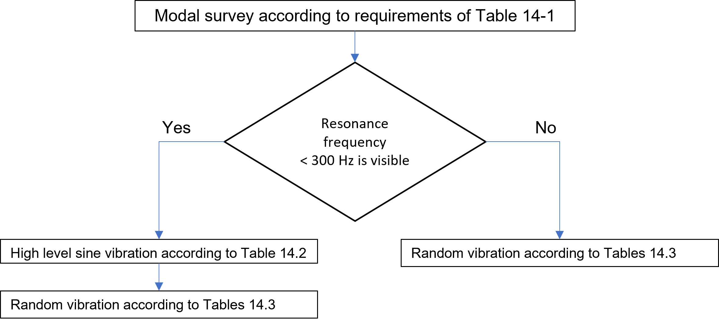 ECSS-Q-ST-70-61_1510966Figure 14-1:Vibration test flow chart
ECSS-Q-ST-70-61_1510967The PCB design and mechanical mounting including fittings such as stiffeners, frames or spacers shall be representative of the flight model.
ECSS-Q-ST-70-61_1510968The mechanical mounting configuration of the PCB for the vibration tests shall be identified.
ECSS-Q-ST-70-61_1510969In order to take into account test samples imperfections, notching may be used to reduce non-representative mechanical over stresses provided that the following two conditions are met:
- Notching is justified to the Approval Authority, and
- Internal notching is identified in the vibration test report.
ECSS-Q-ST-70-61_1510970Minimum vibration levels shall be as specified in Table 14-1, Table 14-2 and Table 14-3.
ECSS-Q-ST-70-61_1510971The vibration levels and duration during verification shall fulfil the project requirements
ECSS-Q-ST-70-61_1510972A modal survey shall be performed to detect any primary resonance frequency. - 1 Modal survey can be done with sine or random vibration
- 2 It is a good practice, for generic applications, that the verification board exhibits a primary resonant frequency in the range of 500 Hz - 800 Hz.
ECSS-Q-ST-70-61_1510973For sine modal survey, the conditions shall be as defined in Table 14-1a.
ECSS-Q-ST-70-61_1510974For random modal survey, the conditions shall be as defined in Table 14-1b.
ECSS-Q-ST-70-61_1510975High level sine vibration may be omitted, provided that the resonance frequency is above 300 Hz for both the verification board and flight model
ECSS-Q-ST-70-61_1510976Transfer function shall be issued from modal survey and presented to customer.
ECSS-Q-ST-70-61_1510977Input vibration levels shall be measured at the interface between the vibration plate and the PCB.
ECSS-Q-ST-70-61_1510978The response acceleration of the assembled PCB shall be monitored and recorded during testing.
ECSS-Q-ST-70-61_1510979The accelerometers shall be placed on the PCB as well as on the base plate to determine the acceleration of the PCB.
It is a good practice to mount the accelerometers on the PCB area of largest deflection.
ECSS-Q-ST-70-61_1510980Vibration testing shall be performed in the three orthogonal axes: one out-of-plane and two in-plane.
ECSS-Q-ST-70-61_1510981The severity of the vibration test shall not be less than that shown in Table 14-2 and Table 14-3.
ECSS-Q-ST-70-61_1510982Table 14-1: Modal survey conditions
|
Table 14-1a - Sine survey
|
|
Table 14-1b - Random survey
| ||
|
Amplitude
|
0,5 g (zero to peak)
|
|
Range (Hz)
|
Level
|
|
Frequency range
|
10 Hz to 2000 Hz
|
|
10 Hz- 2000 Hz
|
5,10-4 g2/Hz
|
|
Sweep rate
|
2 octaves/minute
|
|
Global levels: 1 g r.m.s.
|
|
|
Direction
|
X, Y and Z axis
|
|
X, Y and Z axis
|
1 min/axis
|
|
|
|
|
Frequency sampling = 2 Hz
|
|
ECSS-Q-ST-70-61_1510983Table 14-2: Minimum severity for sine vibration testing
|
|
Axis
|
Frequency range
|
PSD level
|
Sweep rate
|
|
Spacecraft
|
All
|
25 - 100
|
25 g
|
1
|
|
100 - 200
|
15 g
|
1
| ||
|
Duration: 1 cycle up from 25 Hz to 200 Hz
| ||||
|
Launchers
|
All
|
10 - 16
|
10 mm
|
1/3
|
|
16 - 60
|
10 g
|
1/3
| ||
|
60 - 70
|
22,5 g
|
1/3
| ||
|
70 - 200
|
22,5 g
|
2
| ||
|
200 - 2000
|
10 g
|
2
| ||
|
Duration: 1 cycle up from 10 Hz to 2000 Hz
| ||||
ECSS-Q-ST-70-61_1510984Table 14-3: Minimum severity for random vibration testing
|
|
Axis
|
Frequency range[Hz]
|
PSD level
|
Global level
|
|
Spacecraft
|
Parallel to PCB
|
20 - 100
|
+ 6 dB/oct.
|
27,1 g r.m.s.
|
|
100 - 800
|
0,5 g2/Hz
| |||
|
800 - 2000
|
- 3 dB/oct.
| |||
|
Perpendicular to PCB
|
20 - 100
|
+ 6 dB/oct.
|
28,5 g r.m.s.
| |
|
100 - 500
|
1,0 g2/Hz
| |||
|
500 - 2000
|
- 6 dB/oct.
| |||
|
Duration: 5 minutes per axis
| ||||
|
Launchers
|
All
|
20 - 60
|
+ 3 dB/oct.
|
20,0 g r.m.s.
|
|
60 - 1000
|
0,27 g2/Hz
| |||
|
1000 - 2000
|
- 6 dB/oct.
| |||
|
Duration: 5 minutes per axis
| ||||
Mechanical shock
ECSS-Q-ST-70-61_1510985Mechanical shock test shall be performed in assembly verification for area array components in accordance with requirements in clause 13.3, for solderless assemblies in accordance with requirements in clause 13.6 and for the following components:
- Relay
- Quartz
- Magnetic components (RM)
- Transformer and self
- Hybrid
- Tantalum capacitor
- Heavy or large component
- Optical components
- Low insertion force DIP socket
- Semiconductors (IC) components, Hybrid components, relays, capacitors with cavities
The list of components is taken from Table 17-1 of ECSS-E-HB-32-25A (14July2015) that is reproduced in this Standard as Table 14-4.
ECSS-Q-ST-70-61_1510986For components listed in requirement 14.9a, assembly verification shall be made with functional testing to be capable to identify degradation due to shock tests.
ECSS-Q-ST-70-61_1510987The levels and duration of the shock shall be provided in the verification report.
ECSS-Q-ST-70-61_1510988The mechanical shock levels shall be set to meet the intended mission with margin.
ECSS-Q-ST-70-61_1510989Mechanical shock may be omitted if it can be demonstrated that the design has robust margin or proven heritage.
Table 14-4: Shock sensitive electronic components vs. failure modes (Table reproduced from ECSS-E-HB-32-25A)
|
Electronic components
|
Failure modes
| |||
|
Mode 1
|
Mode 2
|
Mode 3
|
Remarks
| |
|
Relay
|
Bouncing
|
Temporary or permanent transfer
|
Non reversible mechanical damage
|
|
|
Quartz
|
Relief of residual stress in the quartz
|
Solder overstress or adhesive crack at clip interfaces
|
Broken crystal
|
Quartz are usually mounted on a damping material
|
|
Magnetic components (RM)
|
Crack initiation in ferrite
|
Electrical lead wire rupture
|
|
The internal part is fragile, in particular if the component is composed of ferrite or ceramic
|
|
Hybrid
|
Adhesive rupture at substrate level or other small part level (getter, absorber)
|
Crack in glass feed-thru
|
Packaging or lid structural failure
|
Packaging is often made of brittle material
|
|
Tantalum capacitor
|
Bending of the PCB leading reversible electrical peak of current due to local destruction of the dielectric
|
Bending of the PCB leading to internal over-stresses with non-reversible total destruction by short circuit - Avalanche phenomenon
|
Tantalum capacitor can also be of large dimensions, hence with same failure modes as for heavy/large components
|
|
|
Heavy or large component
|
For heavy components (> 5 gr), overstress at the attachment due to loads, e.g. capacitor, transformer, shielded components …
|
For large components, overstress at the attachment due to PCB bending
|
|
|
|
Optical components
|
Fibre optic pigtail cleavage
|
Damaged fibre surface in connectors
|
|
|
|
Low insertion force DIP socket
|
Disjunction of the component
|
|
|
|
|
Semiconductors (IC) components, Hybrid components, relays, capacitors with cavities
|
Dislodging of mobile particle
|
|
|
Particles are detected by a PIND test
|
Damp heat test
ECSS-Q-ST-70-61_1510990Damp heat test shall be performed as part of the verification programme for solderless processes according to clause 13.6.
ECSS-Q-ST-70-61_1510991Damp heat test conditions shall be (93 ± 3) % at (40 ± 3) °C for 240 hours in compliance with the Annex C of ECSS-Q-ST-70-14.
Temperature cycling test
ECSS-Q-ST-70-61_1510992The test specimen shall be temperature cycled in an air circulating or inert gas purged chamber.
ECSS-Q-ST-70-61_1510993Before the start of the temperature cycling, the test specimen shall be baked out to remove the internal humidity according to clause 7.3.
ECSS-Q-ST-70-61_1510994The bake-out may be part of the first temperature cycle.
ECSS-Q-ST-70-61_1510995The temperature cycling shall be between 55 (-5/+0) C and +100 (-0/+5) C.
ECSS-Q-ST-70-61_1510996The first temperature cycle shall be hot.
ECSS-Q-ST-70-61_1510997The rate of temperature change during the temperature cycle shall not exceed 10 C per minute.
Higher ramp rates reduce the stresses in the solder joint but increase the stresses within the ceramic materials.
ECSS-Q-ST-70-61_1510998The soak time at each temperature extreme shall be a minimum of 15 minutes.
ECSS-Q-ST-70-61_1510999The monitoring thermocouple shall be attached to the surface of the printed circuit board.
ECSS-Q-ST-70-61_1511000The number of thermal cycles shall be in accordance with:
- clause 13.2 for general verification programme,
- clause 13.3 for assembly verification of ceramic area array components,
- clause 13.4 for assembly verification with electrical testing procedure,
- clause 13.5 for verification programme with reduced temperature range, and
- clause 13.6 for verification for solderless components.
The number of thermal cycles can be higher for SMD, PTH or AAD, based on specific mission requirements.
Temperature cycling test with reduced temperature range
ECSS-Q-ST-70-61_1511001Temperature cycling with reduced temperature range shall be performed as part of the special verification programme in accordance with requirements in clause 13.5.
ECSS-Q-ST-70-61_1511002The stresses during temperature cycling may be reduced by modification of the temperature cycling conditions as follows:
- Decreasing the thermal range during temperature cycling by increasing the minimum temperature from the nominal one, or
- decreasing the thermal range during temperature cycling by decreasing the maximum temperature from the nominal one, or
- decreasing the temperature cycling gradient from the nominal one, or
- any combination of 1 to 3 above.
The modifications refer to changes from the nominal temperature cycling conditions as described in requirements 14.11d and 14.11f.
ECSS-Q-ST-70-61_1511003The temperature cycling may be performed in several steps, with different conditions in the different steps.
A typical stepwise temperature cycling test is to perform the cycling in 2 steps as follows:
- Step 1: Temperature range tailored so that the minimum and maximum temperature on board level during the on-ground qualification conditions are covered including the minimum and maximum temperatures during cold start, non-operating and operating, as required for the intended mission. Number of cycles in this step tailored such that the on-ground qualification conditions are covered at least with a safety margin of 2. The lower temperatures often result in largest stresses, and it is therefore good practice to cover cold start conditions in this first step so that the number of cycles at the larger temperature range are minimized. Example: 20 cycles between -40°C/+85°C with a gradient of 2°C/min and a dwell time of 15 minutes corresponds to 15,5 cycles of -55°C/+100°C with a gradient of 10°C/min as calculated with the equation in requirement 14.12g.
- Step 2: Temperature range tailored so that the minimum and maximum temperature on board level during the in-orbit conditions are covered. Number of cycles in this step tailored such that steps 1 and 2 in total correspond to the nominal temperature cycling range that is required for the type of components being verified, typically 500 cycles, when re-calculated with the modified Coffin-Manson (Norris-Landzberg) equation.
Example: 981 cycles between -10/+100°C with a gradient of 10°C/min or slightly lower and 15 minutes of dwell time. 981 such cycles correspond to 484,8 cycles -55/+100°C with gradient ~10°C/min, as calculated with the equation in requirement 14.12g.Thus the cycling during step 1 and step 2 in total covers the full 500 cycles (15,5 + 484,8 = 500,3) required for surface mounted components as required by requirement 13.2.1cc.* 2 The reason behind dividing the temperature cycling in different steps is to decrease the risk of thermally overstressing the assembly while not prolonging the schedule more than necessary. - 3 It is recommended to perform the tailoring of the temperature cycling such that the envelope of all intended mission requirements can be covered. A case-by-case trade-off between cost, schedule and risk is though often needed.
ECSS-Q-ST-70-61_1511004The total number of cycles shall be tailored such that all the steps in total correspond to the nominal number of thermal cycles with nominal temperature cycling range that is required for the type of components being verified.
ECSS-Q-ST-70-61_1511005The temperature conditions during temperature cycling shall cover the minimum and maximum board temperatures seen by the component in the intended mission profile including on ground qualification testing.
ECSS-Q-ST-70-61_1511006The corresponding number of thermal cycles for the on-ground qualification and in-orbit environment shall be covered at least with a safety margin of 2.
Temperature on board level are taken into account during all the on-ground qualification conditions including the minimum and maximum temperatures during cold start, non-operating and operating, as required for the intended missions.
ECSS-Q-ST-70-61_1511007The modified Coffin-Manson (Norris-Landzberg) equation used for the calculation of the equivalent thermal cycles shall be the following:
where:
AF = Acceleration factor between lab and field conditions
Tmax and Tmin = Maximum and minimum temperatures [Kelvin]
∆T = Temperature difference between Tmax and Tmin
f = Frequency of the cycling when considering each plateau and the gradients [cycles/24h]
The coefficients specified are valid for soldering with SnPb solder only.
Life test
ECSS-Q-ST-70-61_1511008Life test shall be performed as part of the assembly verification for solderless components in accordance with requirements in clause 13.6.
ECSS-Q-ST-70-61_1511009Life test conditions shall be 2000 hours at 125 °C or at maximal operational temperature during flight mission.
Final visual inspection
ECSS-Q-ST-70-61_1511010Visual inspection of each verification sample shall be made using the list of nonconformance criteria of clause 12.3.
ECSS-Q-ST-70-61_1511011Prior to microsectioning, the components shall be in conformance with the dimensional and solder fillet requirements of clause 8,clause 9 and clause 10.
ECSS-Q-ST-70-61_1511012Any identified nonconformance during the visual inspection specified in 14.14a, before any aging test, shall lead to rejection of the verification sample.
ECSS-Q-ST-70-61_1511013Any identified nonconformance during the visual inspection specified in 14.14a, after any aging test, shall be recorded in the traveller sheet of the verification sample.
ECSS-Q-ST-70-61_1511014In the case of visual failures, an analysis shall be performed to identify if the failure results from the component or the assembly process.
ECSS-Q-ST-70-61_1511015The identified nonconformances of 14.14d should be classified in acceptable or unacceptable depending on performed test flow.
* After the environmental test campaign, some defects are acceptable. For example disturbed solder joints are typical after verification programme and are acceptable provided that the microsectioning acceptance criteria are fulfilled. In case of visible cracks in the solder joints, it is difficult to know the crack length from external visual inspection only. Cracks in solder joints can therefore be acceptable provided that the microsectioning acceptance criteria are fulfilled.
ECSS-Q-ST-70-61_1511016The nonconformances identified in 14.14b and 14.14d shall be notified to the Approval Authority within one week.
Microsection
Microsection facilities
ECSS-Q-ST-70-61_1511017The Approval Authority shall make available a list of laboratories available to perform microsection.
The list of available laboratories is on ESCIES website, see www.escies.org, Technologies - ESA SMT Verification: ESA-TECMSP-MO-013165 “ESA recommended microsectioning facilities”.
ECSS-Q-ST-70-61_1511018Microsections shall be performed by a laboratory specified in 14.15.1a except the case specified in the requirement 14.15.1c.
ECSS-Q-ST-70-61_1511019When in-house or other non-listed microsection facilities are used, the supplier shall demonstrate the following:
- the capability of the laboratory on representative samples including chip components, LCCs and FPs as well as conformal coating.
- a report with associated microsections sent to the Approval Authority for review and assessment of quality of microsectioning.
In accordance with ESA memo ESA-TECMSP-MO-013161. See www.escies.org, Technologies - ESA SMT Verification.
Microsections location
ECSS-Q-ST-70-61_1511020At least one microsection shall be made per assembly configuration after environmental testing on each type of component, size and assembly processes and soldering processes.
- 1 Different soldering processes and different staking, bonding or conformal coating are examples of different configurations.
- 2 Successive polishing planes can be performed.
ECSS-Q-ST-70-61_1511021Microsectioning of repaired sample shall cover the manually soldered assembly, provided the same configuration.
ECSS-Q-ST-70-61_1511022The microsection shall be done on the component having the worst solder joint appearance as identified at MIP2.
ECSS-Q-ST-70-61_1511023For assembly sensitive components, 5 (five) components shall be microsectioned per assembly configuration.
ECSS-Q-ST-70-61_1511024Additional microsections may be requested by the Approval Authority in case of cracks or other features detected during the first microsection sampling..
ECSS-Q-ST-70-61_1511025Adhesive bonding for thermal or mechanical purpose underneath a component shall be microsectioned.
ECSS-Q-ST-70-61_1511026The microsections of the component shall be done as specified in Table 14-5.
Microsection acceptance criteria
General
ECSS-Q-ST-70-61_1511027The integrity of the assembly shall be assessed by microsectioning.
Integrity covers PCB, solder joints, adhesives and packages.
ECSS-Q-ST-70-61_1511028After microsectioning, the microsections shall be in compliance with requirements of Table 14-5.
ECSS-Q-ST-70-61_1511029The microsection shall be inspected with a magnification of 50x to 200x except the case specified in the requirement 14.15.3.1d
ECSS-Q-ST-70-61_1511030The microsection for components with small stand-off should be inspected with magnification up to 500x.
Examples of small stand-off components are LCCs, chip resistors and capacitors, QFN.
ECSS-Q-ST-70-61_1511031In case the microsection shows a crack more than 75 % of acceptable crack, the component type shall be classified as assembly sensitive.
ECSS-Q-ST-70-61_1511032If the component type is classified as assembly sensitive, according to requirement 14.15.3.1e, all remaining components from verification boards shall be microsectioned in order to confirm that acceptance criteria are still fulfilled.
For a first verification of a new component not identified as assembly sensitive, 3 components are sufficient.
ECSS-Q-ST-70-61_1511033The Approval Authority shall have access to the moulded microsection and pictures.
ECSS-Q-ST-70-61_1511034The verification board and associated microsections shall be stored for a period of at least ten years.
- 1 It is good practice to store the boards until end of mission.
- 2 Boards can assist the analysis of in-orbit failures.
Acceptance criteria
ECSS-Q-ST-70-61_1511035Cracks in the solder joint outside of the critical zone shall be accepted.
ECSS-Q-ST-70-61_1511036Cracks in the mechanical bonding shall not be accepted.
ECSS-Q-ST-70-61_1511037Cracks in the mechanical bonding may be accepted provided that the criteria defined in Table 14-5 are met and accepted by Approval Authority.
ECSS-Q-ST-70-61_1511038Cracks in the mechanical staking shall not be accepted.
ECSS-Q-ST-70-61_1511039Cracks in the mechanical staking may be accepted provided that one of the following items are met:
- at completion of verification the criteria defined in Table 14-5 are met and accepted by Approval Authority.
- after vibration and a minimum of 50 thermal cycles, visual inspection show absence of cracks in the staking and photos of staking are provided.
ECSS-Q-ST-70-61_1511040Cracks in the thermal bonding shall not be accepted.
ECSS-Q-ST-70-61_1511041Cracks in the thermal bonding may be accepted at the completion of the verification testing when they are perpendicular to PCB surface plane.
ECSS-Q-ST-70-61_1511042Any damage to the component beyond the ones acceptable by the component datasheet shall be identified as a verification failure.
ECSS-Q-ST-70-61_1511043Damages outside of what is allowed in the component data sheet may be acceptable providing acceptance of Approval Authority.
ECSS-Q-ST-70-61_1511044Table 14-5: Component microsection location and acceptance criteria
|
Component type
|
Example component
|
Cross section planes
|
Example of views at min and max magnification
|
Critical Zone definition
|
Acceptance criteria
| |
|

|
Terminal to cross section
|
|
|
red-dotted line indicates critical zone
|
|
|
|
Images in the table are informative examples only. Requirements are specified in text.
| ||||||
|
Radial component
|
CKR capacitors
|
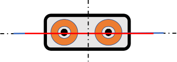 |
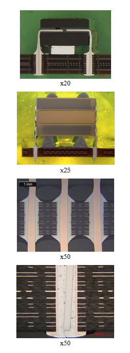 |
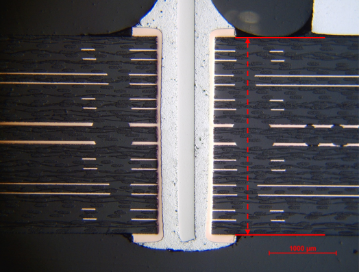
|
The total sum of cracks in the solder joint is less than 25% of critical zone length
| |
|
Axial components
|
CH capacitors
|
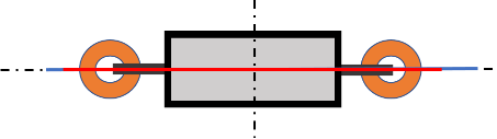 |
||||
|
Stacked capacitors
|
-
|
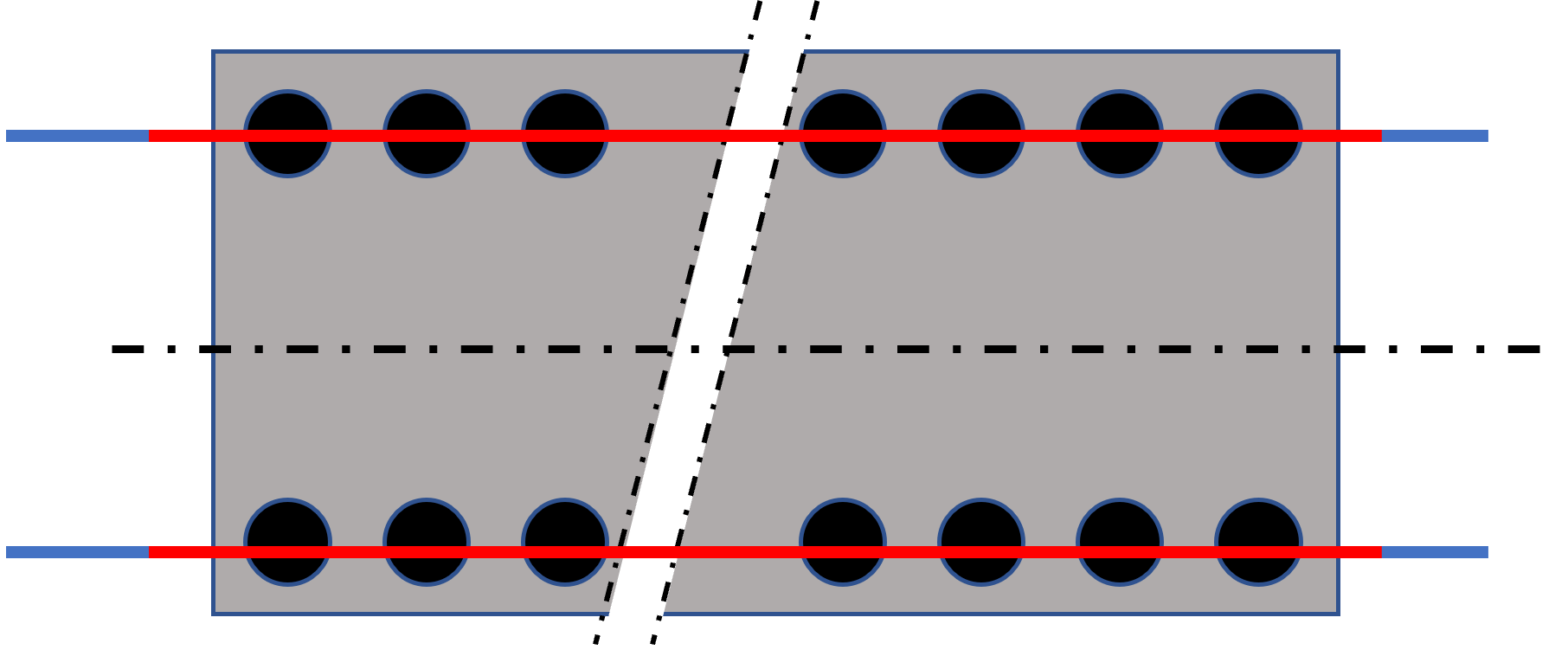
|
||||
|
1 component is necessary:
| ||||||
|
TO package component
|
TO39
|
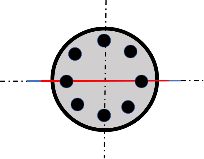
|
||||
|
Microsection in the largest distance between two leads
| ||||||
|
TO package component with metal tab
|
TO254
|
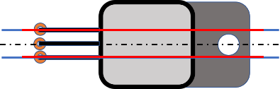
|
||||
|
This package generally contains BeO that can be considered as hazardous for microsectioning. The microsectioning plane might need to be redefined after discussion with the microsectioning laboratory and asses possible health and safety issues.
| ||||||
|
Dual in Line Package (DIL or DIP)
|
Side brazed DIP>24 pins
|

|
-
|

|
The total sum of cracks in the solder joint is less than 25% of critical zone length
| |
|
1 component is necessary:
| ||||||
|
Connectors
|
|
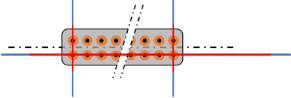
|
- |
|||
|
2 components are necessary:
| ||||||
|
Radial magnetics
|
1553 transformers
|
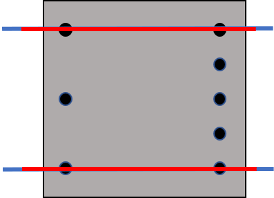 |
- |
|||
|
Sculptured flexible
|
|
- |
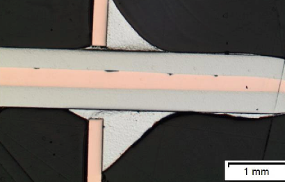
|
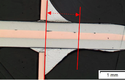
|
No crack in the solder joint on the solder side at completion of the test.
| |
|
Rectangular and square end-capped or end-metallized component with rectangular body
|
Chip resistors
|
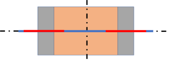
|
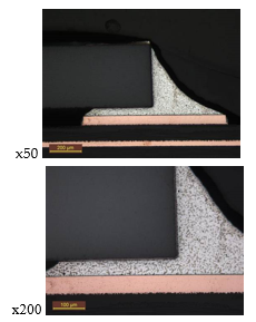
|
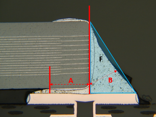
|
The total sum of cracks in the solder joint is less than 60% of A+B and no crack in fillet area F
| |
|
Chip capacitors
|
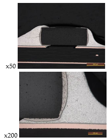
|
|||||
|
Resistor array
|

|
- |
||||
|
Rectangular and square end-capped or end-metallized metallic component with rectangular body,
|
CSM
|
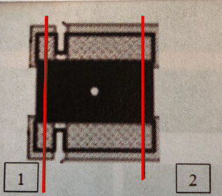
|

|
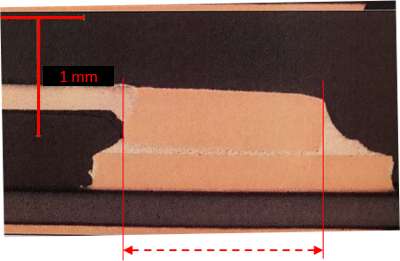
|
The total sum of cracks in the solder joint is less than 33% of lap connection
| |
|
Cylindrical and square end-capped components with cylindrical body
|
MELF
|

|
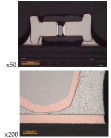
|
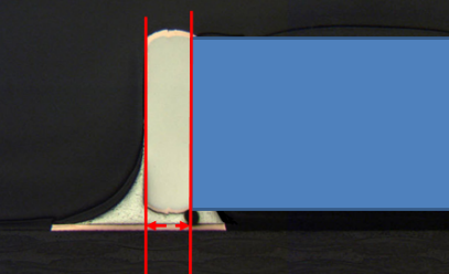
|
The total sum of cracks in the solder joint is less than 33% of critical zone length |
|
|
Bottom terminated chip component
|
Coil
|
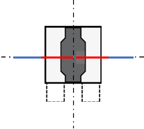
|

|
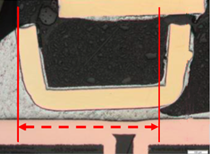
|
The total sum of cracks in the solder joint is less than 33% of lap connection
| |
|
Component with Inward formed L-shaped leads
|
Tantalum chip capacitor
|
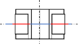
|
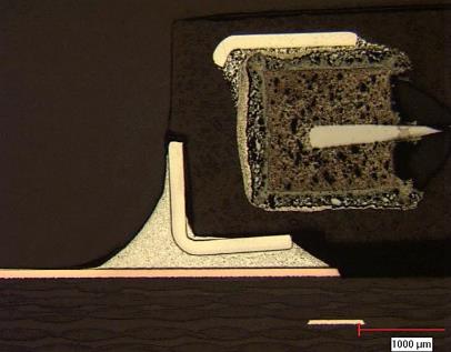
|

|
The total sum of cracks in the solder joint is less than 33% of critical zone length |
|
|
Leadless component with plane termination
|
SMD0.5, SMD1, SMD2, SMD0.2
|
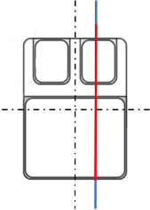
+ X-ray prior to microsectioning |
Absence of cracks in the ceramic to be checked by visual inspection prior to microsectioning |
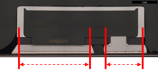
|
The total sum of cracks in the solder joint is less than 33% of lap connection
| |
|
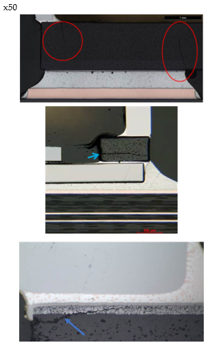
|
||||||
|
Leaded component with plane termination
|
DPAK/TO252
|
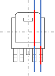 |
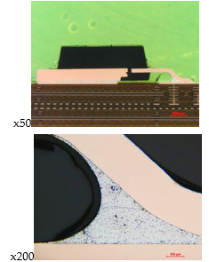
|
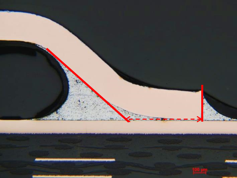
|
For lead, the total sum of cracks in the solder joint is less than 33% of critical zone length.
| |
|
X-ray+ micro section (lead + plane) Microsection plane in on edge Additional microsection depending on lead configuration (different dimensions or shape) |
||||||
|
Leadless ceramic chip carrier component
|
LCC3
|
|

|
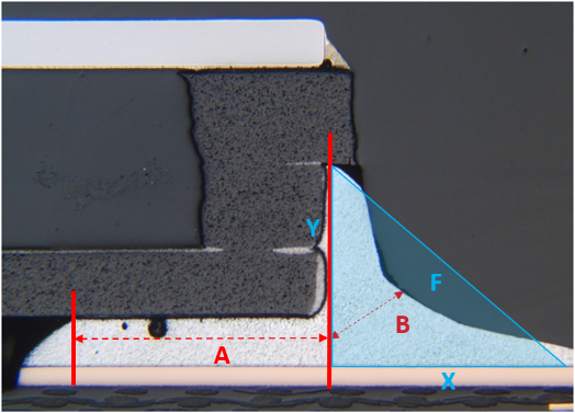
|
The total sum of cracks in the solder joint length is less than 70% of A+B
| |
|
With ground connection (microsection to be done in the middle of castellation)
| ||||||
|
|
||||||
|
Without ground connection
| ||||||
|
LCC with terminations on 2 faces
|
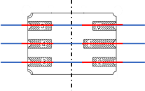
|
|||||
|
all terminals to be microsectioned
| ||||||
|
LCC with termination on 4 faces
|
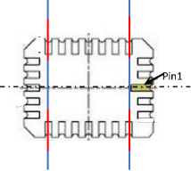
|
|||||
|
No lead Quad Flat Pack
|
QFN
|
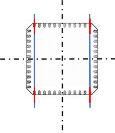
|
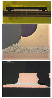
|
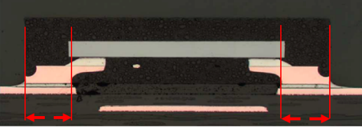
|
The total sum of cracks in the solder joint is less than 33% of critical zone
| |
|
When thermal plane is present, the third microsection is in the middle axis:
| ||||||
|
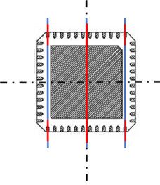
|
||||||
|
Flat pack and Gull-wing leaded component with round, rectangular, ribbon leads, Moulded magnetics
|
CQFP + MQFP
|
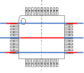
|
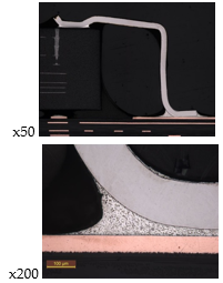
|
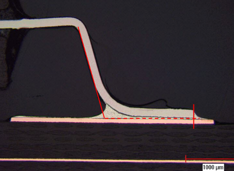
|
The total sum of cracks in the solder joint is less than 33% of critical zone length
| |
|
Centre micro-section to be done only when component is bonded.
|
Similar magnification to be applied for the assessment of the bonding lines.
| |||||
|
FP, SO, SOIC
|
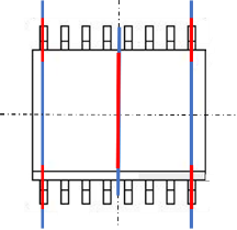
|
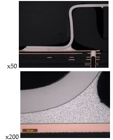
|

|
The total sum of cracks in the solder joint is less than 33% of critical zone length Absence of crack in the adhesive |
||
|
Centre micro-section to be done only when component is bonded.
| ||||||
|
FP with spider leads
|
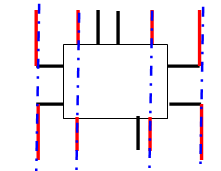
|
|||||
|
SOT 23
|
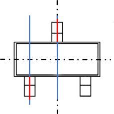
|

|

|
|||
|
Flat pack and Gull-wing leaded component with round, rectangular, ribbon leads, Moulded magnetics
| ||||||
|
1553 interface transformers or specific transformers
|
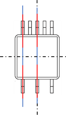
|
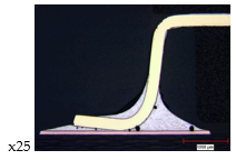
|
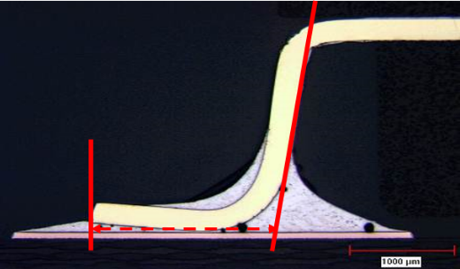
|
The total sum of cracks in the solder joint is less than 33% of critical zone length Absence of crack in the adhesive |
||
|
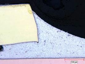
|
||||||
|
Microsection plane in one edge. Additional microsection depending on lead configuration (different dimensions or shape)
| ||||||
|
Flat pack and Gull-wing leaded component with round, rectangular, ribbon leads, Moulded magnetics
|
|
|
|
|
|
|
|
TSOP
|

|
|
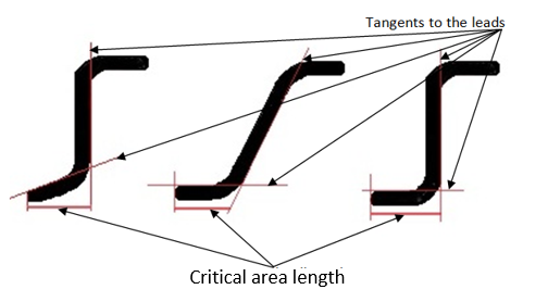
|
The total sum of cracks in the solder joint is less than 10% of critical zone length |
||
|
“J” leaded component
|
ceramic leaded chip carriers (CLCC) and plastic leaded chip carriers (PLCC).
|
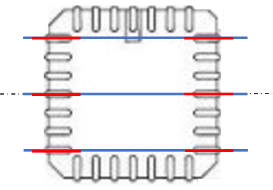
|
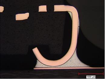
|
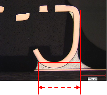
|
The total sum of cracks in the solder joint is less than 33% of critical zone length |
|
|
Components with ribbon terminals without stress relief (flat lug leads)
|
|
|

|

|
The total sum of cracks in the solder joint is less than 33% of critical zone length |
|
|
Stacked modules components with leads protruding vertically from bottom
|
|
Can be reduced to two microsections when package is ≤ 50 leads |
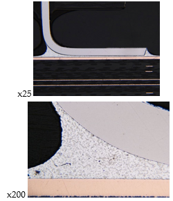
|
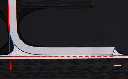
|
The total sum of cracks in the solder joint is less than 33% of critical zone length
| |
|
Area Array components (Capability Phase only)
|
CCGA
|
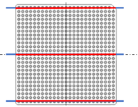
|
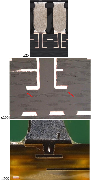
|
Not applicable |
For capability samples only: Acceptance criteria as defined in clause 13.3.2. |
|
|
Presence of cracks in the laminate and interconnection of microvia
| ||||||
|
Solderless
|
Component, interposer and PCB
|
Cross sections of PCB pad in the contact area Cross section of interposer in the contact area Cross section of component plating |
No picture available for now
|
|
Acceptance criteria as defined in clause 13.6. |
|
Microsection acceptance criteria for ceramic chip capacitors
ECSS-Q-ST-70-61_1511045Solder joint of ceramic chip capacitors after microsectioning shall be in compliance with Table 14-5.
ECSS-Q-ST-70-61_1511046For ceramic chip capacitors damages inside the component after microsectioning shall be in compliance with Table 14-6.
- 1 The cracks in the ceramic observed at completion of assembly verification may be located either on the top terminations or on the bottom terminations. The cause of the cracks depends on their location on the component.
- 2 Cracks in the ceramic material at the bottom terminations can have several different root cause:
- Mechanical stress from bending the PCB during handling, depanelization, integration of the PCB in the unit or from mechanical testing.
- Thermal shock during soldering due to excessive solder tip temperature or the solder tip touching the component termination.
Due to the different root causes the repeatability of bottom side ceramic cracks are low.
The risk of bottom side terminations can be reduced by for example pre-heating the board before soldering, and using lower soldering tip temperatures, as also noted in requirement 10.2.5q.
- 3 Cracks in the ceramic material at the top terminations can be caused by the pull stress occurring at cold temperatures during temperature cycling. Verification with reduced temperature range in accordance with clause 13.5 reduce the amount and size of such top side cracks.
EIA-469 issue E criteria for minimum insulation of the cover plate has been used to define the acceptance criteria of these cracks at the completion of assembly verification. EIA 469 issue E requires a minimum insulation of 80 µm for 50 V and above.
The as received thickness of the cover plate vary between different chip capacitor values and ratings, as well as between different batches. The ceramic cracks could furthermore occur on all corners of the part. Therefore the acceptability of ceramic cracks is assessed by projecting the worst crack seen on all 4 corners of the component and also by comparing it to the flight batch of the component.
- 4 For chip capacitors it is good practice to perform the verification on the capacitance value used which has the thinnest cover plate and most densely packed dielectric planes.
- 5 EIA-469 issue E has been used to define the acceptance criteria for delaminations.
ECSS-Q-ST-70-61_1511047Table 14-6: Acceptance criteria for internal defects in ceramic chip capacitors after microsectioning
|
Type of defect
|
Location
|
Case
|
Figure
|
Additional note
|
Acceptance criteria
|
|
Crack in solder joint
|
N/A
|
N/A
|
N/A
|
N/A
|
See clause 14.15.3 and Table 14-5.
|
|
Crack in ceramic
|
Bottom terminations
|
N/A
|
N/A
|
Due to the different root causes the repeatability of bottom side ceramic cracks are low.
|
No cracks in the ceramic on the bottom termination.
|
|
Top terminations
|
Case 1a: Crack curving towards the termination on same side and remaining cover plate thickness ≥ 80µm
|
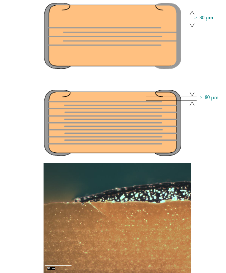
|
Example: Assembly verified component has minimum 100 µm cover plate as received and a ceramic crack which reduces the insulation distance with 15 µm, i.e. 85 µm remaining insulation which is acceptable. This would in addition be acceptable justification for all chip capacitors of the same type, provided they have minimum 95 µm cover plate as received at all 4 corners.
|
Crack is curving towards the termination on same side.
| |
|
Crack in ceramic
|
Top terminations
|
Case 1b: Crack curving towards the termination on same side and remaining cover plate thickness < 80µm
|
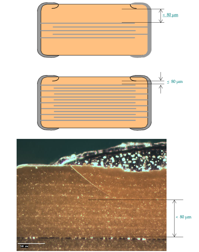
|
The review of ceramic cracks is assessed by projecting the worst crack seen on all 4 corners of the component and also by comparing it to the flight batch of the component.
|
Not acceptable.
|
|
Crack in ceramic
|
Top terminations
|
Case 2a: Straight crack with ≤45° angle to electrode plane and no projected crossing of opposite electrodes
|
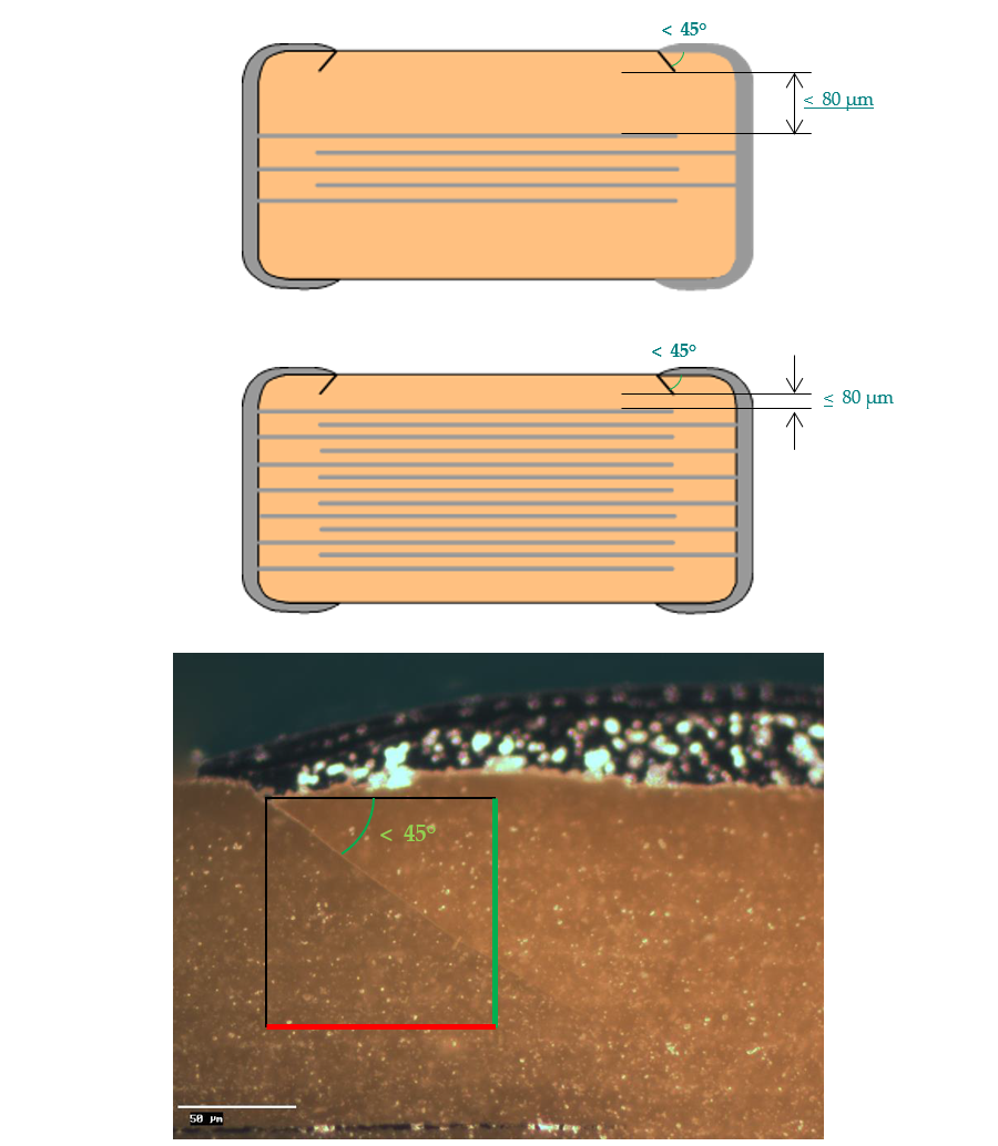
|
It is good practice to draw a quadrat from the root of the ceramic crack to assess the crack angle.
|
Crack has maximum 45° angle to electrode plane.
|
|
Crack in ceramic
|
Top terminations
|
Case 2b: Straight crack with ≤45° angle to electrode plane and projected crossing of opposite electrodes
|
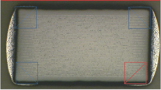
|
The review of ceramic cracks is assessed by projecting the worst crack seen on all 4 corners of the component and also by comparing it to the flight batch of the component.
|
Not acceptable.
|
|
Crack in ceramic
|
Top terminations
|
Case 3: Straight crack with >45° angle to electrode plane
|
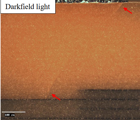
|
The review of ceramic cracks is assessed by projecting the worst crack seen on all 4 corners of the component and also by comparing it to the flight batch of the component.
|
Not acceptable.
|
|
Delamination
|
Any termination
|
Chip capacitors size ≥1210
|
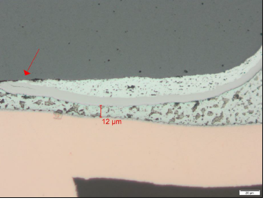
|
The delamination can have an impact on the size of the cracks in the solder joint as they provide stress relief.
|
No delamination larger than 130 µm.
|
|
Chip capacitors size <1210
|

|
N/A
|
Not acceptable.
| ||
|
Chip capacitors with flexible terminations
|
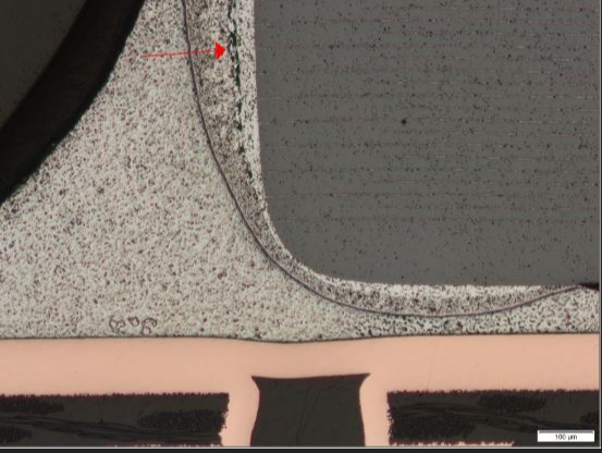
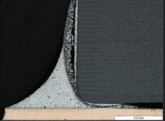 |
The risk of delamination in the vertical part of the flexible polymer layer can be reduced by the decreasing the solder height.
|
Not acceptable.
|
Anomalies in PCB and sculptured flex during verification
ECSS-Q-ST-70-61_1511048After verification testing the acceptance criteria of ECSS-Q-ST-70-60 clause 10.3 and 10.5 shall apply, except for the case specified in requirements 14.16b and 14.16c.
- 1 ECSS-Q-ST-70-60 includes acceptance criteria for cracks in dielectrics for PTH.
- 2 ECSS-Q-ST-70-60 Table 10-25 includes acceptance criteria for pad lift types and Table 10-26 for dielectric cracks.
ECSS-Q-ST-70-61_1511049Anomalies outside the conditions specified in requirement 14.16a may be accepted provided that at least one of the following conditions is met: - Presence of anomaly also during PCB procurement, either on the PCB coupons or in certificate.
- Presence of anomaly also on a spare non-assembled nor tested PCB.
- Presence of anomaly also on a spare footprint, included on the verification board, showing that the defect was not caused by the assembly processes.
It is good practice to include additional footprints on the verification board, which are not populated, to assist failure investigations.
ECSS-Q-ST-70-61_1511050Cracks in the dielectrics under SMT footprints, outside the conditions specified in requirement 14.16a, may be accepted provided that the remaining insulation distance of the flight PCB is in conformance with the PCB definition dossier.
ECSS-Q-ST-70-61_1511051Cracks in the Printed Circuit Board that have not been identified in the clause 10 of ECSS-Q-ST-70-60 shall be unacceptable.
ECSS-Q-ST-70-61_1511052Defects, such as footprint lifting, cracks in laminate, cracks in via, cracks of tracks, PCB delamination shall be recorded as a nonconformance and analysed.
Outsourcing
General
ECSS-Q-ST-70-61_1511053A supplier may be designated for outsourcing from a customer provided that the following conditions are met:
- Outsourcing activities are limited to degolding and pretinning, lead forming, hand soldering, bonding, staking and conformal coating.
- The manufacturing processes to be performed are included in the customer's PID approved by the Approval Authority.
- The manufacturing at the supplier site is performed with the same materials as the one used by the customer.
- The manufacturing at the supplier site is performed in compliance with the manufacturing procedures of the customer PID.
- In case the outsourcing includes lead forming activities, the demonstration that lead geometry is identical are provided to the customer.
- The customer is responsible for the assembly carried out by the supplier,
- The supplier fills in the manufacturing traveller of the customer.
- In case the supplier is not equipped to fill in the manufacturing traveller of the customer, he can use his own manufacturing traveller provided that it has been reviewed and accepted by the customer.
- All operators and inspectors working at the supplier site are trained and certified according to clause 17.8 and being active in their certification status.
- All operators and inspectors working at the supplier site for the customer as outsourcing are trained on customer applicable PID procedures and certified by the instructor of the customer.
For the requirement 15.1a.3, ideally those materials are provided in the kitting.
ECSS-Q-ST-70-61_1511054The operators and inspectors shall work only on one set of specified process procedures at a time at the supplier site.
ECSS-Q-ST-70-61_1511055The customer shall issue and maintain a certification matrix of the certification status of the supplier’s operators and inspectors including the name of the instructor and the supplier assembly contact point name.
ECSS-Q-ST-70-61_1511056The customer PID shall identify the certification matrix with the associated names of the supplier involved personnel.
ECSS-Q-ST-70-61_1511057The manufacturing dossier of the boards and unit shall identify the operations performed by the supplier.
ECSS-Q-ST-70-61_1511058The customer shall appoint a person in charge of NCRs issued by customer and supplier.
ECSS-Q-ST-70-61_1511059The supplier shall be informed about assembly NCRs in the customer assembly line.
ECSS-Q-ST-70-61_1511060The customer shall conduct an audit at supplier according to clause 13.1.3 to verify the compliance of the assembly line.
ECSS-Q-ST-70-61_1511061The customer shall provide to the Approval Authority the audit report.
ECSS-Q-ST-70-61_1511062In case of modification in the procedures, the supplier operators and inspectors shall be informed, trained, and certified according to requirement 15.1a.10.
ECSS-Q-ST-70-61_1511063KIPs shall be performed by the customer inspector,
ECSS-Q-ST-70-61_1511064The customer shall have a storage, packing and transportation procedure for the hardware manufactured at supplier assembly line,
ECSS-Q-ST-70-61_1511065Incoming inspections of the assembly shall be performed by the customer to verify absence of damage due to the storage, packing and transportation,
ECSS-Q-ST-70-61_1511066Every 4 years the customer shall invite the Approval Authority to participate the audit of the supplier assembly line, in compliance with requirement 13.1.3f.
ECSS-Q-ST-70-61_1511067The customer shall list in its PID the supplier as “outsourcing” to manufacture hardware.
Process identification document (PID)
Overview
The purpose of the PID is to establish a precise reference for the assembly processes approved in accordance with this Standard.The PID provides a standard reference against which any anomalies occurring after the approval can be examined and resolved.### Document preparation
ECSS-Q-ST-70-61_1511068Prior to any start of verification, the supplier shall provide a draft PID to the Approval Authority, in conformance with the DRD in Annex C.
ECSS-Q-ST-70-61_1511069The PID may supersede the requirements from this standard in case supplier can demonstrate that any deviation recorded in the PID is approved by Approval Authority based on tests results.
Approval
ECSS-Q-ST-70-61_1511070The PID shall be submitted to the Approval Authority
ECSS-Q-ST-70-61_1511071The Approval Authority shall approve the PID.
The approval can be achieved by PID signature or minutes of meeting being signed by the Approval Authority.
Contact person
ECSS-Q-ST-70-61_1511072The supplier shall appoint a contact person for assembly topics.
Process identification document update
ECSS-Q-ST-70-61_1511073A PID shall represent the verified manufacturing processes and production controls.
ECSS-Q-ST-70-61_1511074Any proposed change to the PID shall be agreed by the Approval Authority.
ECSS-Q-ST-70-61_1511075At least every two years the supplier shall perform a review of the PID, the summary table and the relevant applicable documents for agreement by the Approval Authority.
ECSS-Q-ST-70-61_1511076The PID shall be managed in accordance with configuration control requirements of ECSS-M-ST-40.
Quality assurance
General
ECSS-Q-ST-70-61_1511077Requirements from clause 5 from ECSS-Q-ST-20 shall apply for "Quality assurance".
Data
ECSS-Q-ST-70-61_1511078Quality records shall be retained for at least ten years, or in accordance with the project contract.
Example of quality records are travellers log, work orders.
ECSS-Q-ST-70-61_1511079Quality records shall be gathered in the Verification report in conformance with the DRD in Annex B.
ECSS-Q-ST-70-61_1511080The following documents, as a minimum, shall be made available to supplier
- PID.
- Audit report established by the Approval Authority.
- Verification report.
Nonconformance
ECSS-Q-ST-70-61_1511081The requirements from clauses 5 and 6 from ECSS-Q-ST-10-09 shall apply for "Nonconformance".
Calibration
ECSS-Q-ST-70-61_1511082Equipment and tools, degolding and pretinning bathes, soldering equipment, and measuring equipment shall be calibrated within a period of one year.
ECSS-Q-ST-70-61_1511083The supplier shall maintain records of the calibration according to clause 5.2.6 of ECSS-Q-ST-20.
ECSS-Q-ST-70-61_1511084A suspected or confirmed tool or equipment failure shall be recorded as a project nonconformance.
The records can aid early detection of a trend towards nonconformance.
ECSS-Q-ST-70-61_1511085Defective or out of calibration date equipment or tools shall be labelled or removed from work areas.
ECSS-Q-ST-70-61_1511086The Approval Authority shall be notified of the nonconformance.
Traceability
ECSS-Q-ST-70-61_1511087The requirements from clause 5.2.5 of ECSS-Q-ST-20 shall apply for traceability.
Workmanship standards
ECSS-Q-ST-70-61_1511088The supplier shall prepare in-house visual workmanship standards to be made available to each operator and inspector.
- 1 Examples are: Satisfactory work samples or visual aids which illustrate the quality characteristics of all types of soldered connection involved in the task.
- 2 The illustrations presented in Annex F and Annex E this standard can be included as part of the examples.
Inspection points
ECSS-Q-ST-70-61_1511089During all stages of the process, the inspection points defined in the manufacturing flow chart shall be carried out.
ECSS-Q-ST-70-61_1511090The inspection shall be performed in conformance with clause 12.
Operators, inspectors and instructors training and certification
ECSS-Q-ST-70-61_1511091Trained and certified personnel shall be employed for soldering operations and inspections.
ECSS-Q-ST-70-61_1511092A training programme shall be developed, maintained and implemented by the supplier to provide excellence of workmanship and personnel skills in soldering.
ECSS-Q-ST-70-61_1511093Records of training, testing and certification status of the operators and inspectors shall be maintained for at least 10 years.
ECSS-Q-ST-70-61_1511094The training programme shall include procedures for the training, internal certification, maintenance of certified status, recertification, and revocation of certified status for soldering and inspection personnel.
ECSS-Q-ST-70-61_1511095Training success shall be based on objective evidence of soldering quality, resulting from practical training and inspection of soldered joints.
ECSS-Q-ST-70-61_1511096Personnel shall be retrained or re-assessed in the following circumstances:
- Repeated quality nonconformance.
- Change in soldering techniques.
- Change in soldering parameters.
- Additional process skills.
ECSS-Q-ST-70-61_1511097The operators performing X-ray inspection shall be trained and in-house certified to perform and assess X-ray results.
ECSS-Q-ST-70-61_1511098Operators, inspectors and instructors shall be certified at an ESA school in compliance with ESA STR-258 or in-house training authorised by the Approval Authority.
ECSS-Q-ST-70-61_1511099Operators and inspectors may be re-certified at an ESA school or by an in-house instructor authorised by the Approval Authority.
The supplier company is responsible for checking the constant visual acuity of its workers i.a.w. ESA STR-258 to maintain certification status of personnel.
ANNEX(normative)Verification programme - DRD
DRD identification
Requirement identification and source document
This DRD is called from ECSS-Q-ST-70-61, requirement 13.1.4a.
Purpose and objective
The purpose of the Verification programme DRD is to detail the requirements for the documentation of the verification programme.### Expected response
Scope and content
ECSS-Q-ST-70-61_1511100The verification programme documentation shall contain as a minimum the following:
- Indication of process of the assembly:
- soldering process
- repair process.
- Substrate information:
- PCB material and manufacturer
- PCB footprint surface finish
- Number of layers
- Thickness
- Build up with identification of signal and full copper plane
- Connection of the footprints to the internal layer representative of the FM
- Location of the components on the PCB
- For through hole component, ratio of hole to lead diameter
- Location of the mechanical fixation or stiffeners if any
- Number of PCB used for the verification programme.
- Materials used
- Solder paste and wire designation, commercial trademark, and composition with associated flux class
- Flux class used for pretinning and soldering
- Conformal coating
- Adhesive, potting, underfill and encapsulants used for mechanical and for thermal purpose
- Solvent
- Others.
- List of components with their materials leads and finish
- Environmental test conditions and facility
- Electrical continuity test specification, procedure
- Verification method Microsection or Electrical monitoring
- Microsection laboratory.
- PID and Manufacturing document process references
- Verification workflow
- Verification by similarity
- Certification status of the operators and inspectors
- Compliance status of the operators and inspectors
- Compliance of the manufacturing room
- Additional information. ECSS-Q-ST-70-61_1511101The content of Verification programme specified in requirement A.2.1a may be tailored for companies already having an approved PID in accordance with this standard.
Special remarks
None.
ANNEX(normative)Verification report - DRD
DRD identification
Requirement identification and source document
This DRD is called from ECSS-Q-ST-70-61, requirement 13.1.6a.
Purpose and objective
The purpose of the Verification report DRD is to summarize all the verification test specifications, procedures and test results which are relevant for the approval of the assembly component verifications.### Expected response
Scope and content
ECSS-Q-ST-70-61_1511102The verification documentation shall contain as a minimum the following:
- Indication of process of the assembly:
- soldering process
- repair process.
- PCB information:
- PCB material and manufacturer
- PCB footprint surface finish
- Number of layers
- Thickness
- Build up with identification of signal and full copper plane
- Connection of the footprints to the internal layer representative of the FM
- Location of the components on the PCB
- For through hole component, ratio of hole to lead diameter
- Location of the mechanical fixation or stiffeners if any
- Number of PCB used for the verification programme.
- Materials used
- Solder paste and wire designation, commercial trademark, and composition with associated flux class
- Flux class used for pretinning and soldering
- Conformal coating
- Adhesive for mechanical, and for thermal
- Solvent
- Others.
- List of components with their materials leads and finish (including traceability).
- Mechanical specification of the component with associated manufacturer specification.
- Environmental test conditions and facility
- Visual inspection report established in conformance with the requirements of clause 12
- Summary of cleanliness test results in conformance with clause 11.1.2 of ECSS-Q-ST-70-61 or equivalent process when applicable
- Tests results concerning the warp (bow) and twist of circuit board in conformance when applicable
- Electrical continuity test report for multilayer boards when applicable
- Verification method Microsection or Electrical monitoring
- Microsection laboratory
- PID and Manufacturing document process references
- Verification workflow
- Verification by similarity
- NCRs
- Certification status of the operators and inspectors
- Compliance status of the operators and inspectors
- Compliance of the manufacturing room
- Quality records
- Additional information.
ECSS-Q-ST-70-61_1511103The verification report shall contain the results of all tests performed according to clauses 12 and 14.
ECSS-Q-ST-70-61_1511104The verification report shall contain photographic evidence of the tested assembled boards where possible.
ECSS-Q-ST-70-61_1511105The verification report shall contain the manufacturing soldering log according to clause 13.2.4.
ECSS-Q-ST-70-61_1511106The verification report shall contain the list of all NCRs referring to assembly and test of verification boards and associated reports.
Special remarks
None.
ANNEX(normative)Process Identification Documentation (PID) - DRD
DRD identification
Requirement identification and source document
This DRD is called from ECSS-Q-ST-70-61 requirement 16.2a.
Purpose and objective
The purpose of the PID is to consolidate the overall management, process and facilities utilised during the manufacturing and verification of the assembly.
Expected response
Scope and content
SECTION 1: Document Format
ECSS-Q-ST-70-61_1511107The PID shall contain the following information about the Document Format:
- Cover page: document title, document reference, revision number and date, page numbering, signing of Production and Quality representatives,
- Follow-up of PID updates: registration of PID updates indicating the nature of the update and the sections and pages updated,
- Purpose and scope of the document,
- Table of contents. SECTION 2: Manufacturing control
ECSS-Q-ST-70-61_1511108The PID shall contain the Manufacturing control flow chart of the verified assembly.
- 1 This illustrates the various stages of procurement, manufacturing and inspection operations specific to this technology in a flow chart format.
- 2 It can be used to identify, among others:
- the operation,
- the body responsible for its implementation,
- related documents: (only their reference),
- procurement specifications (for materials),
- acceptance inspection procedures (for materials and components),
- manufacturing procedures,
- manufacturing and quality control procedures during and at the end of production.
- storage documentation
SECTION 3: Specifications
ECSS-Q-ST-70-61_1511109The PID shall contain the following information about Specifications:
- List of procurement specifications, assembly procedures and inspection procedures concerning the technology dealt within the PID, including the precise title, the reference or number, the revision number and date of each document
- Printed circuit design rules in compliance with requirements from ECSS-Q-ST-70-12.
- General Quality Assurance documents relating to the technology. SECTION 4: Organisation
ECSS-Q-ST-70-61_1511110The PID shall contain the following information about Organisation:
- Represented as a flow chart: organization of the company, organization of production department and organization of the quality Department.
- Focal point and PID responsible,
- Operators and inspectors’ certification methodology. SECTION 5: Manufacturing traveller or log file
ECSS-Q-ST-70-61_1511111The PID shall contain as a minimum the following information about the Manufacturing traveller or log file:
- The sequencing of the various operations in their logical order of execution,
- The references of the documents referred to and used during these operations,
- The references of the Quality documents to trace the various batches of material used (record reference), together with the workstations and tools employed,
- The signatures of the various actors with the date on which the task was completed. Section 6: List of verified technologies
ECSS-Q-ST-70-61_1511112The PID shall contain as a minimum the following information about the list of verified technology:
- List of materials,
- Temperature and time profiles for the soldering machines used in the verification,
- List of verified components per assembly configuration,
- List of assembly sensitive components,
- List of components with limited project verification,
- For limited project verification, non-compliance with clause 13 shall be clearly identified. SECTION 7: Description of production line
ECSS-Q-ST-70-61_1511113The PID shall contain as a minimum the following about the Description of production line:
- Layout of premises with associated surface area, with indication of location of production machines and quality inspection,
- Working environment; cleanliness class, ambient temperature limits, humidity, and positive pressure limits for each type of activities. SECTION 8: List of equipment
ECSS-Q-ST-70-61_1511114The PID shall contain a list of all machines and tools utilised during the manufacturing activity.
SECTION 9: List of laboratory services
ECSS-Q-ST-70-61_1511115The PID shall contain range and capability of supporting laboratory services.
SECTION 10: Project assembly heritage
ECSS-Q-ST-70-61_1511116The PID shall contain a list of assembled board with associated assembly process by year manufactured in accordance with the PID.
Special remarks
None.
ANNEX(normative)Assembly Summary Table - DRD
DRD identification
Requirement identification and source document
This DRD is called from ECSS-Q-ST-70-61, requirement 13.1.7d.
Purpose and objective
The purpose of the assembly summary table is to consolidate the approval status of the boundary conditions for the verification activity.
An assembly summary table is issued for each assembly process.
Expected response
Scope and content
ECSS-Q-ST-70-61_1511117The assembly summary table shall include the following data:
- Assembly processes
- PID reference with issue
- Solder type for machine reflow and for hand assembly
- Conformal coating
- Substrate type
- Component data.
An example of a component type preparation and mounting configuration table is given in Figure D-1.
Special remarks
None.
|
Component family
|
Package
|
Manufacturer
|
Package dimensions
|
Bonding material (under component)
|
Staking material (edge or corner)
|
Termination material
|
Lead finish
|
Pitch
|
Nominal Termination thickness (mm)/ Nominal width
|
In-House degolding / pretinning
|
In-house lead forming
|
Artificial stand-off
|
Final report
|
|
Ceramic chip
|
C0603 Type I
|
|
Length, width
|
NA
|
NA
|
|
Sn/Pb
|
NA
|
NA
|
No
|
N/A
|
No
|
|
|
Ceramic
|
C0603 Type II
|
|
|
|
|
|
|
|
|
|
N/A
|
|
|
|
Ceramic resistor
|
R0805
|
|
|
NA
|
NA
|
|
Sn/Pb
|
NA
|
NA
|
No
|
N/A
|
No
|
|
|
Diode
|
D5-B
|
|
|
|
|
|
|
|
|
|
N/A
|
|
|
|
Tantalum capacitors
|
|
|
|
|
|
|
|
|
|
|
|
|
|
|
IC
|
FP10 Bottom brazed
|
|
|
yes
|
One the side
|
Alloy42
|
Gold
|
1,27
|
0,25
|
yes
|
yes
|
NA
|
|
|
CQFP
|
CQFP196 top brazed
|
|
|
|
|
Kovar
|
|
|
|
|
No
|
|
|
Figure: Example of component type preparation and mounting configuration
ANNEX(normative)Visual workmanship standards for through hole component
Soldered stud terminals
NOTE: See clause 10.3.3 for details and allowed exceptions
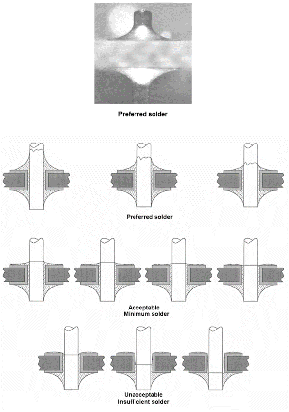 ECSS-Q-ST-70-61_1511118 Figure: Soldered stud terminals
Soldered turret terminals
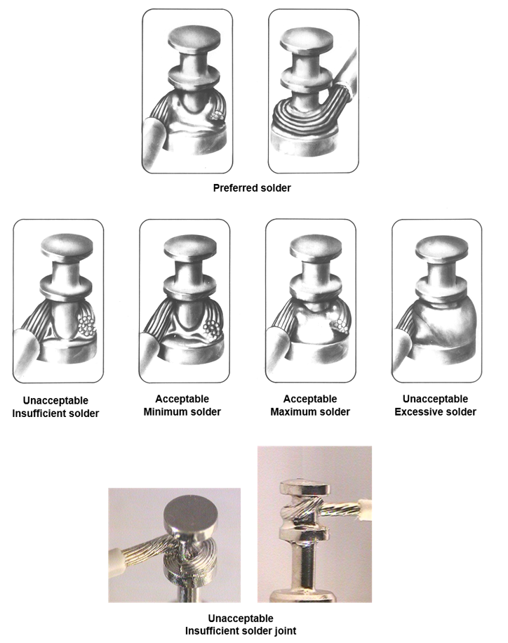 ECSS-Q-ST-70-61_1511119Figure: Soldered turret terminals with single conductors
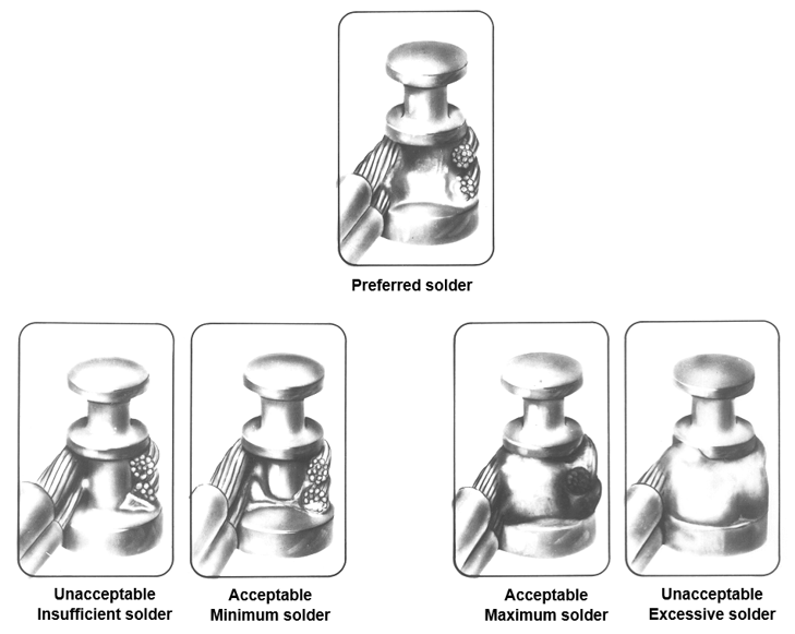 ECSS-Q-ST-70-61_1511120Figure: Soldered turret terminals with twin conductors
Soldered bifurcated terminals
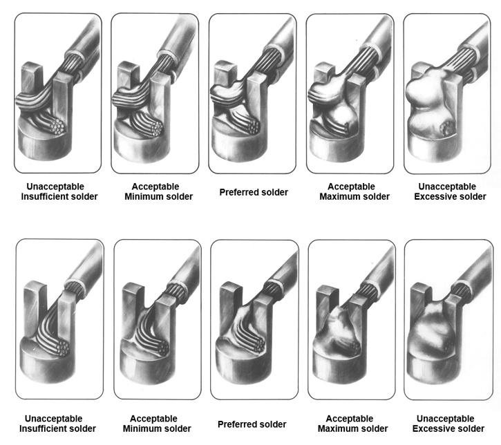 ECSS-Q-ST-70-61_1511121Figure: Soldered bifurcated terminals
Soldered hook terminals
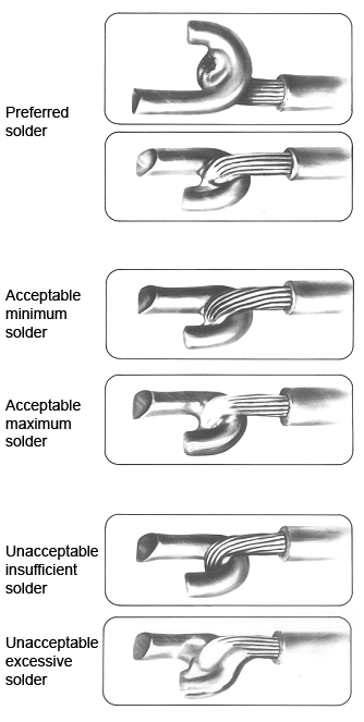 ECSS-Q-ST-70-61_1511122Figure: Soldered hook terminals
Soldered cup terminals
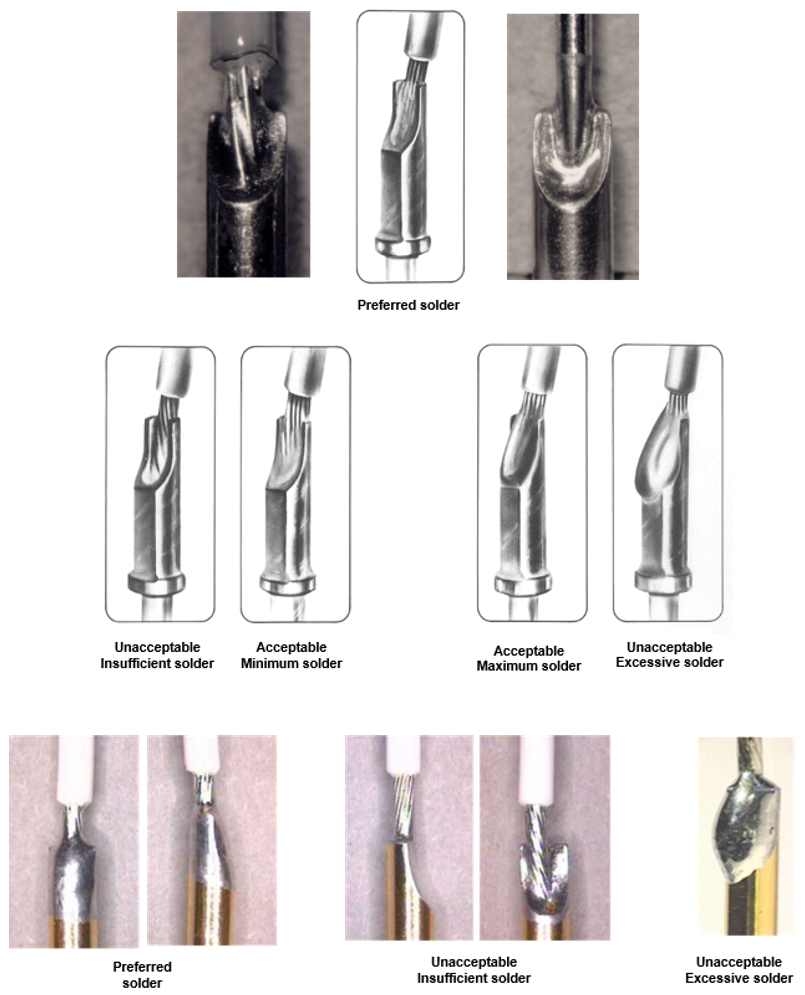 ECSS-Q-ST-70-61_1511123Figure: Soldered cup terminals
Miscellaneous examples of soldered wires
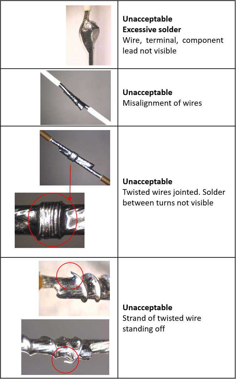 Figure: Examples of unacceptable soldered wires
Soldered wire to shielded cable interconnections
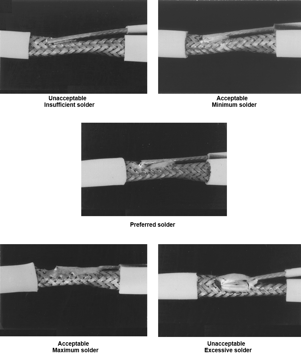 ECSS-Q-ST-70-61_1511124Figure: Hand soldered wire to shielded cable interconnections
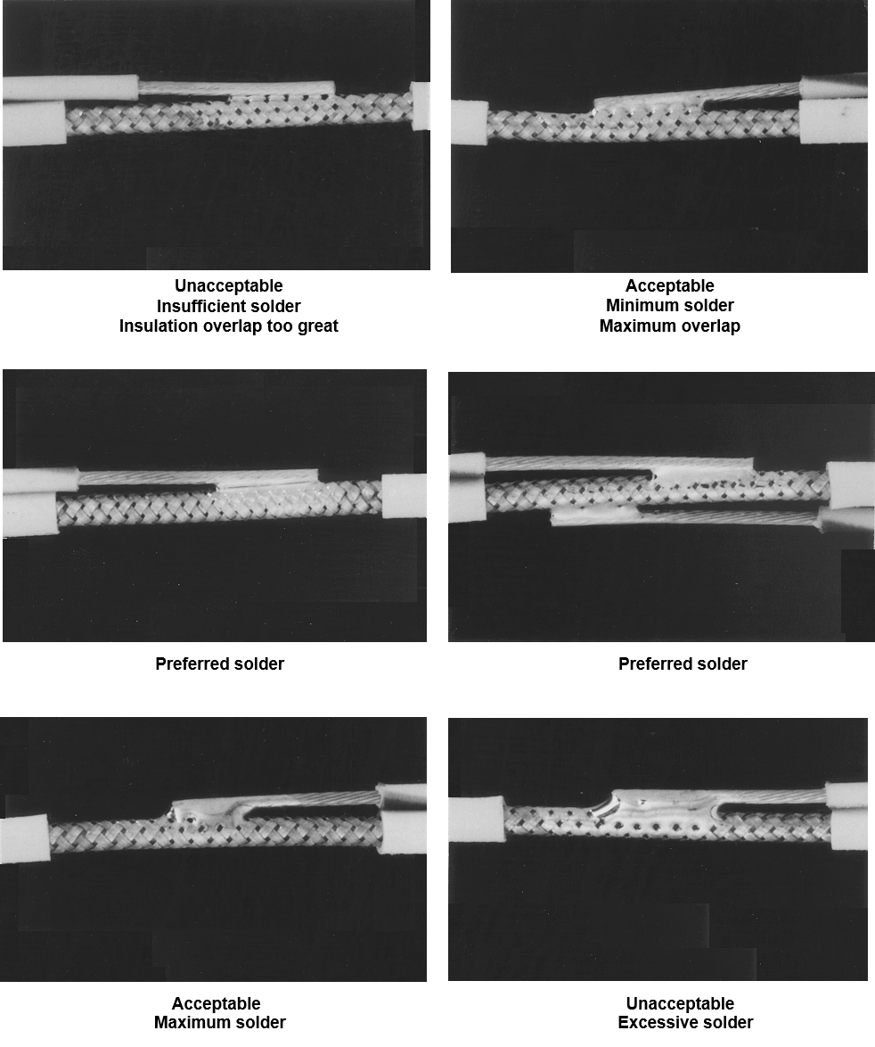 ECSS-Q-ST-70-61_1511125Figure: Hand soldered wire to shielded wire interconnections
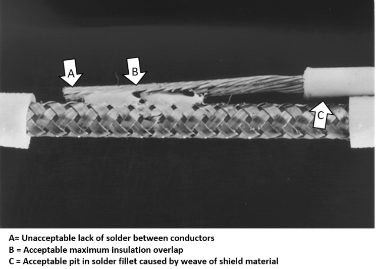 ECSS-Q-ST-70-61_1511126Figure: Hand soldered wire interconnections - details of defects
Assembly of Dual in Line Package
|
Component |
Picture |
Criteria |
|
Vertical leads |
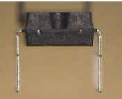
|
Acceptable |
|
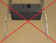
|
Unacceptable |
|
|
No solder on tapered portion of leads |
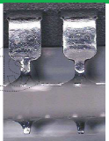
|
Acceptable |
|
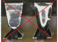
|
Right termination is unacceptable |
|
|
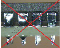
|
Unacceptable |
ANNEX(informative)Visual and X-ray workmanship standards for SMDs
Workmanship illustrations for standard SMDs
Rectangular and square end-capped or end-metallized component with rectangular body
The following photos are provided as support material to the figures given in clause 10.4.2.
|
Criteria
|
Component
|
Picture
|
|
Preferred
|
Chip capacitor
|
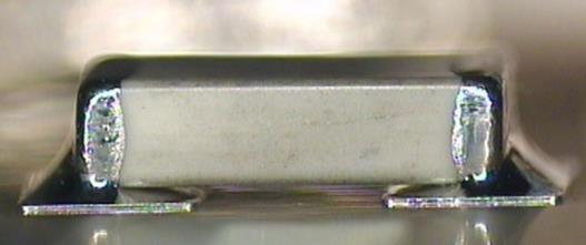
|
|
Acceptable (min)
|
Chip capacitor
|
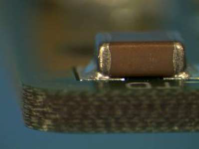
|
|
Acceptable (max)
|
Chip capacitor
|
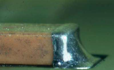
|
|
Criteria
|
Component
|
Picture
|
Comment
|
|
Unacceptable
|
Chip capacitor
|
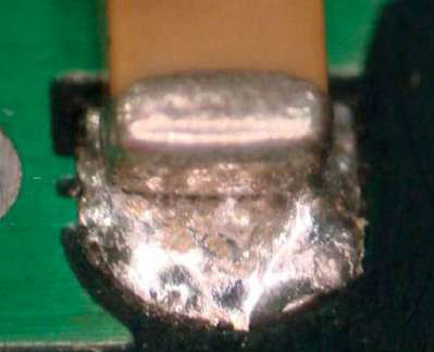
|
No wetting
|
|
Chip resistor
|

|
Excessive tilt
| |
|
Chip capacitor
|

|
Tombstone effect
| |
|
Chip capacitor
|
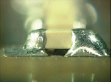
|
Excessive solder joint and asymmetry of solder joints
|
Cylindrical and square end-capped components with cylindrical body
The following photos are provided as support material to the figures given in clause 10.4.3.
|
Criteria
|
Component
|
Picture
|
|
Preferred
|
MELF
|
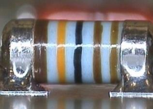
|
|
Acceptable (min)
|
MELF
|
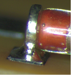
|
|
Acceptable (max)
|
MELF
|
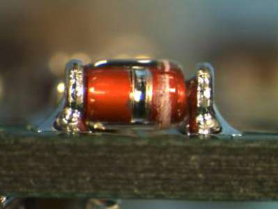
|
|
Criteria
|
Component
|
Picture
|
Comment
|
|
Unacceptable
|
MELF
|
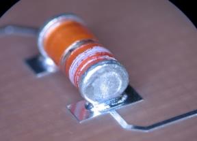
|
Insufficient solder joint
|
|
MELF
|
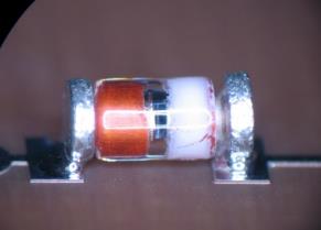
|
Excessive overhang
|
Component with Inward formed L-shaped leads
The following photos are provided as support material to the figures given in clause 10.4.5.
|
Criteria
|
Component
|
Picture
|
|
Preferred
|
Tantalum capacitor
|
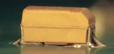
|
|
Acceptable (min)
|
Tantalum capacitor
|
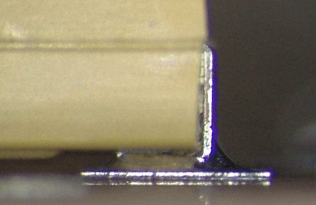
|
|
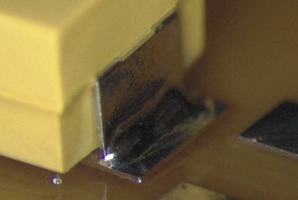
|
||
|
Acceptable (max)
|
Tantalum capacitor
|
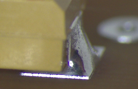
|
|
Criteria
|
Component
|
Picture
|
Comment
|
|
Unacceptable
|
Tantalum capacitor
|
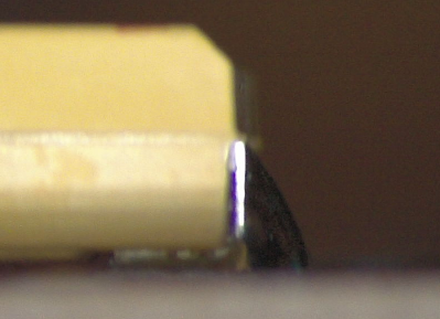
|
max
|
|
Tantalum capacitor
|
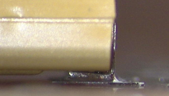
|
min
| |
|
Tantalum capacitor
|
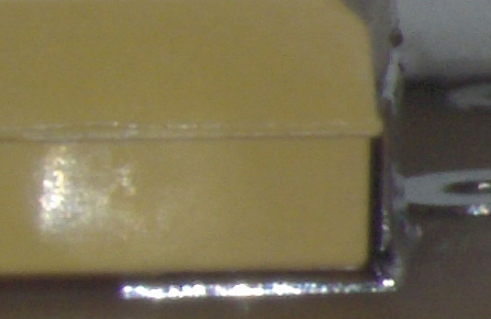
|
not adapted pad with associated insufficient solder fillet |
Leadless component with plane termination
The following photos are provided as support material to the figures given in clause 10.4.6.
|
Criteria
|
Component
|
Picture
|
|
Preferred
|
|
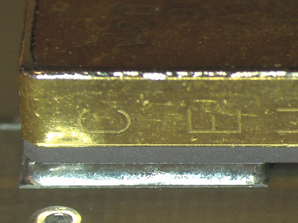
|
|
Acceptable (min)
|
|
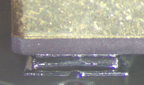
|
|
Acceptable (max)
|
|
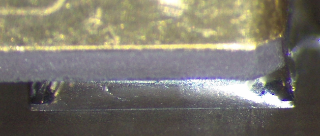
|
|
Criteria
|
Component
|
Picture
|
Comment
|
|
Unacceptable
|
|
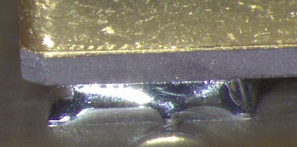
|
max
|
|
|
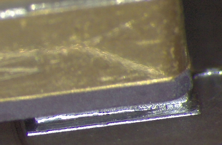
|
min
| |
|
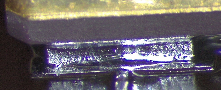
|
Leaded component with plane termination
The following photos are provided as support material to the figures given in clause 10.4.7.
|
Criteria
|
Component
|
Picture
|
|
Preferred
|
D2Pack
|
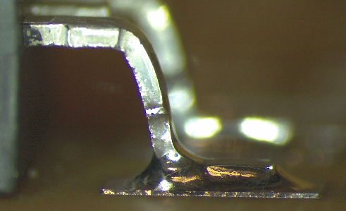
|
|
Acceptable (min)
|
D2Pack
|
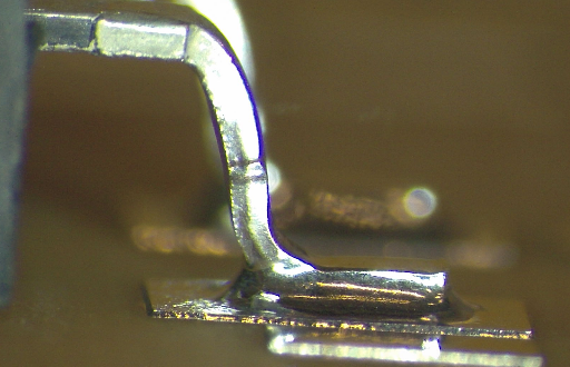
|
|
Acceptable (max)
|
D2Pack
|
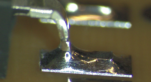
|
|
Criteria
|
Component
|
Picture
|
Comment
|
|
Unacceptable
|
D2Pack
|
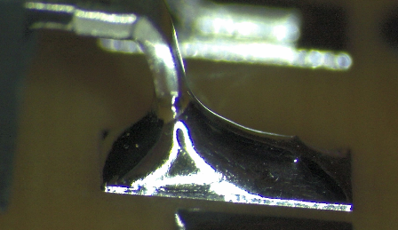
|
Excessive solder
|
|
D2Pack
|
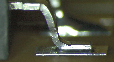
|
Insufficient solder
| |
|
D2Pack
|
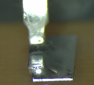
|
Excessive overhang
| |
|
D2Pack
|
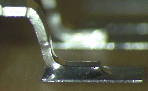
|
Insufficient distance to footprint edge at heel
|
Leadless castellated ceramic chip carrier component
The following photos are provided as support material to the figures given in clause 10.4.8.
|
Criteria
|
Component
|
Picture
|
Comment
|
|
Preferred
|
LCCC
|
No photo available at this time |
|
|
Acceptable
|
LCCC
|
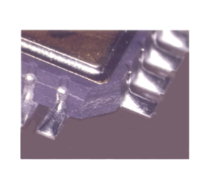
|
|
|
Unacceptable
|
LCCC6
|
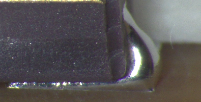
|
Excessive solder
|
|
LCCC6
|
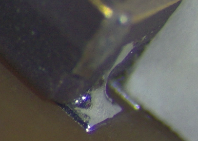
|
Insufficient solder
| |
|
LCCC6
|
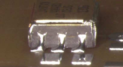
|
Unacceptable overhang
|
Flat pack and Gull-wing leaded component with round, rectangular, ribbon leads
The following photos are provided as support material to the figures given in clause 10.4.10.
|
Criteria
|
Component
|
Picture
|
|
Preferred
|
Flat pack
|
|
|
Acceptable (min)
|
Gull-wing package
|

|
|
Acceptable (max)
|
Gull-wing package
|
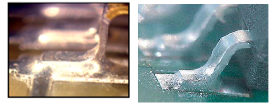
|
|
Criteria
|
Component
|
Picture
|
Comment
|
|
Unacceptable
|
|
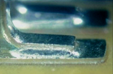
|
Insufficient heel fillet
|
|
|
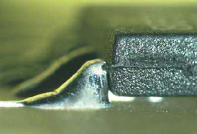
|
Excessive solder
| |
|
|
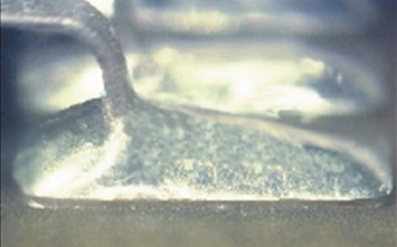
|
Excessive solder
| |
|
Flat pack
|
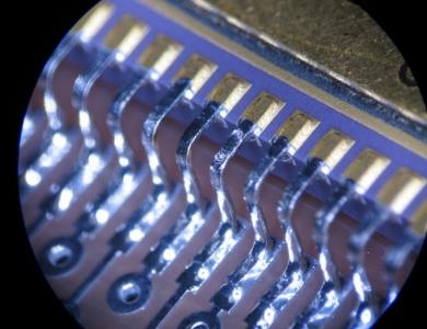
|
Excessing degoldin
|
“J” leaded component
The following photos are provided as support material to the figures given in clause 10.4.11.
|
Criteria
|
Component
|
Picture
|
Comment
|
|
Preferred
|
“J” leaded package
|
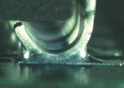
|
|
|
Acceptable (min)
|
“J” leaded package
|

|
|
|
Acceptable (max)
|
“J” leaded package
|
No photo available at this time |
|
|
Unacceptable
|
“J” leaded package
|
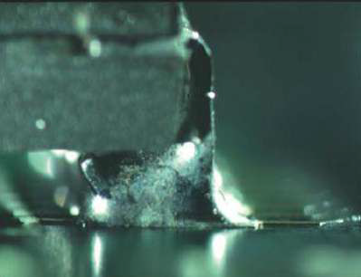
|
Excessive solder joint
|
Area array components
The following photos are provided as support material to the figures given in clause 10.4.14.
|
Criteria
|
Component
|
Picture
|
Comment
|
|
Unacceptable
|
CCGA
|
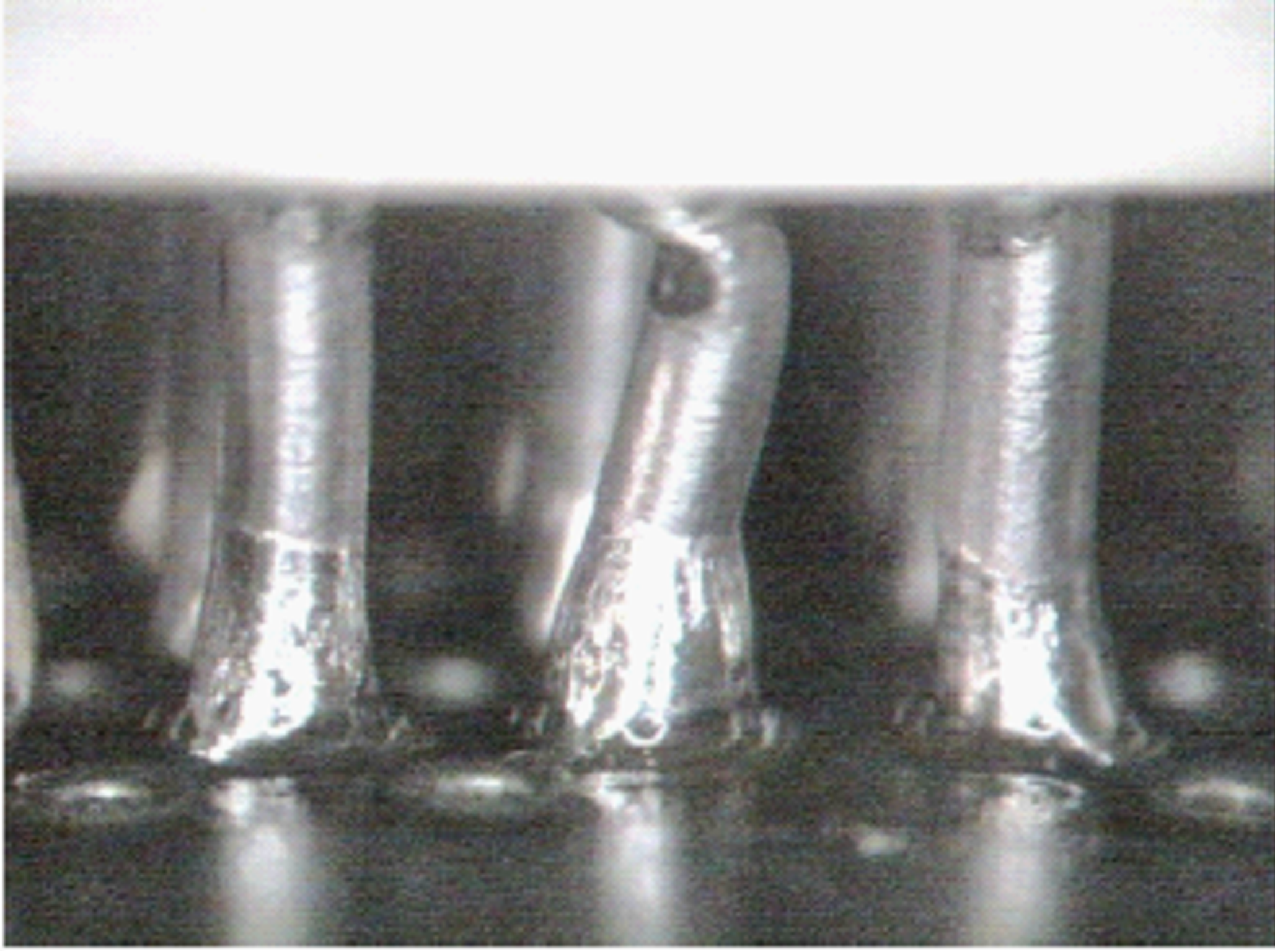
|
Bent column
|
|
CCGA
|
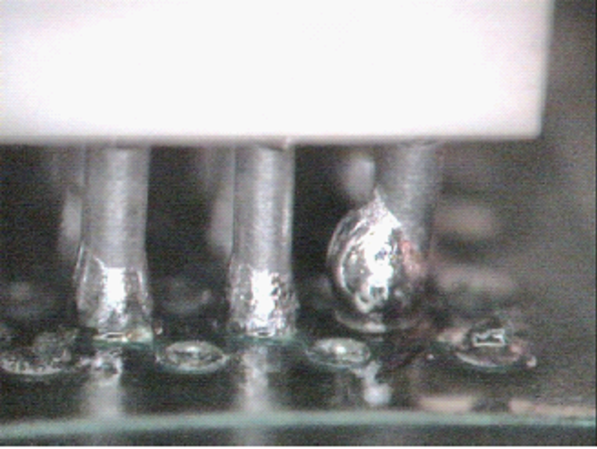
|
Excessive solder joint
|
Miscellaneous soldering defects
|
Criteria
|
Picture
|
Comment
|
|
Unacceptable
|
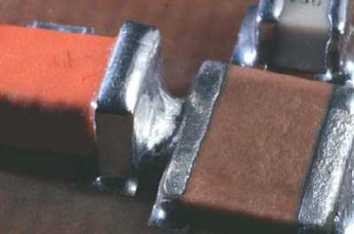
|
Solder bridge between terminals
|
|
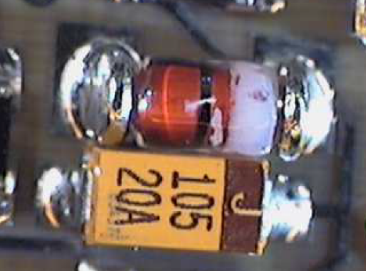
|
Melf misplacement and lack of insulation distance with other component
| |
|
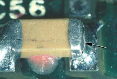
|
Misplacement and fractured solder joint
| |
|
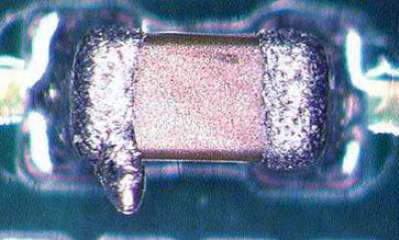
|
Icicle
|
|
Criteria
|
Picture
|
Comment
|
|
Unacceptable
|
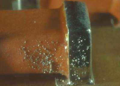
|
Solder microballs
|
|
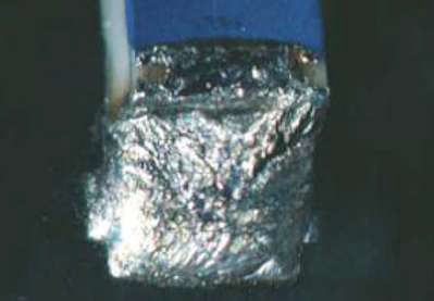
|
Cold wetting
| |
|
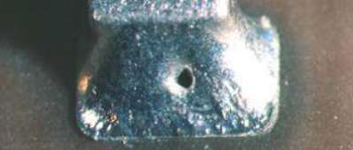
|
Void bottom not visible
|
X Ray Workmanship illustrations for solder flow and voids
|
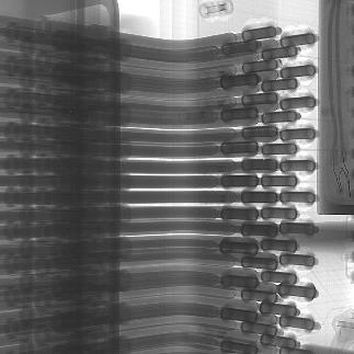
|
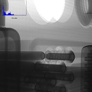
|
|
a) acceptable
|
b) acceptable
|
|
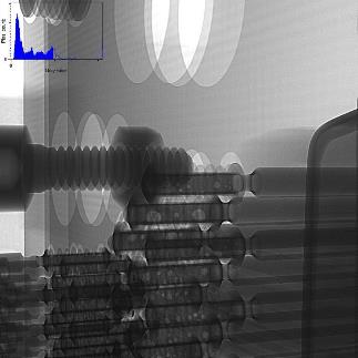
|
|
|
c) acceptable
|
d) acceptable
|
|
|
|
|
e) not acceptable
|
f) acceptable
|
Figure: Examples of acceptable and not acceptable solder flow through and maximum voids during X-ray
X Ray Workmanship illustrations for ball grid array devices
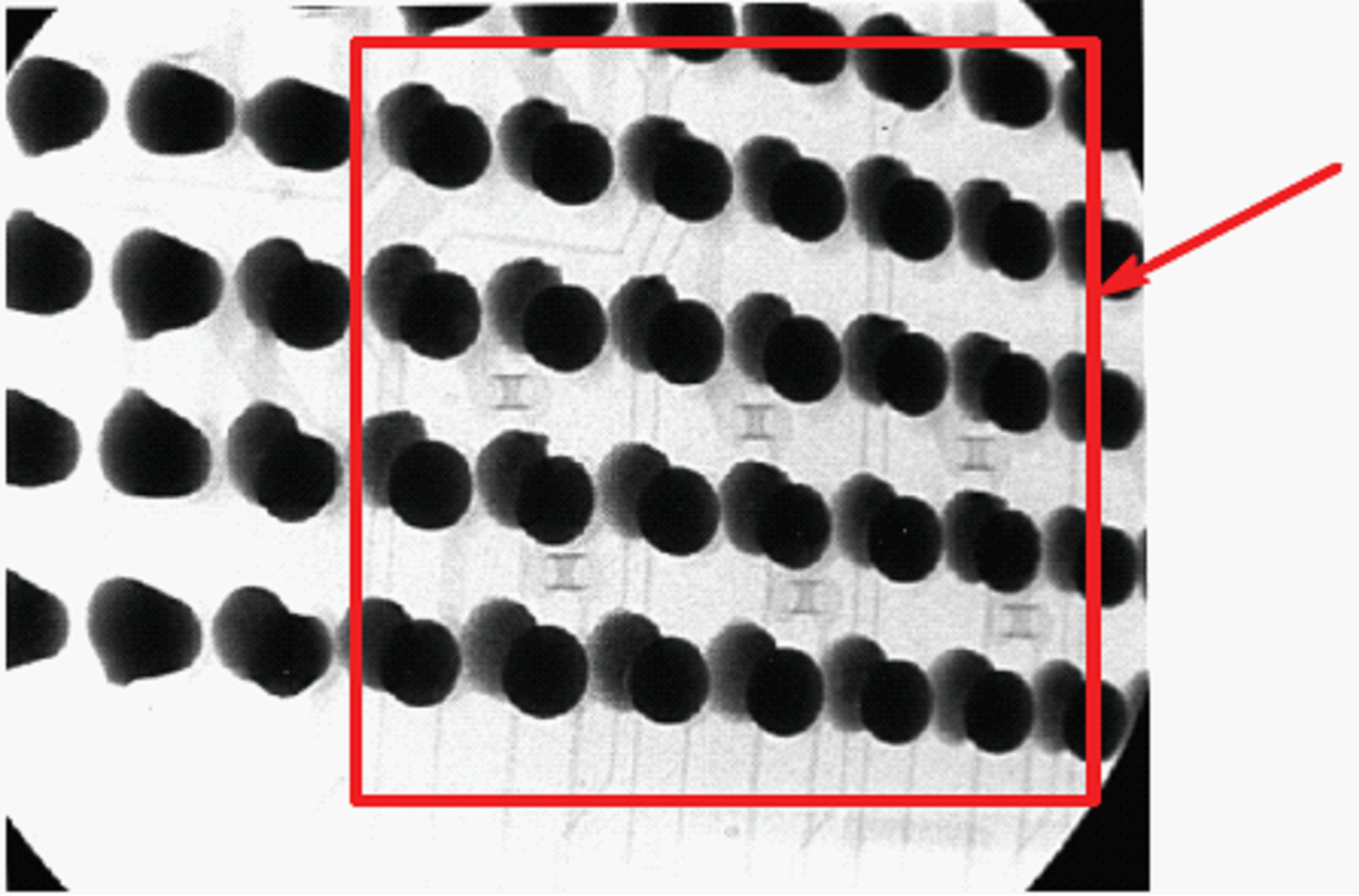 Figure: Angled-transmission X-radiograph showing solder paste shadow due to partial reflow: Reject
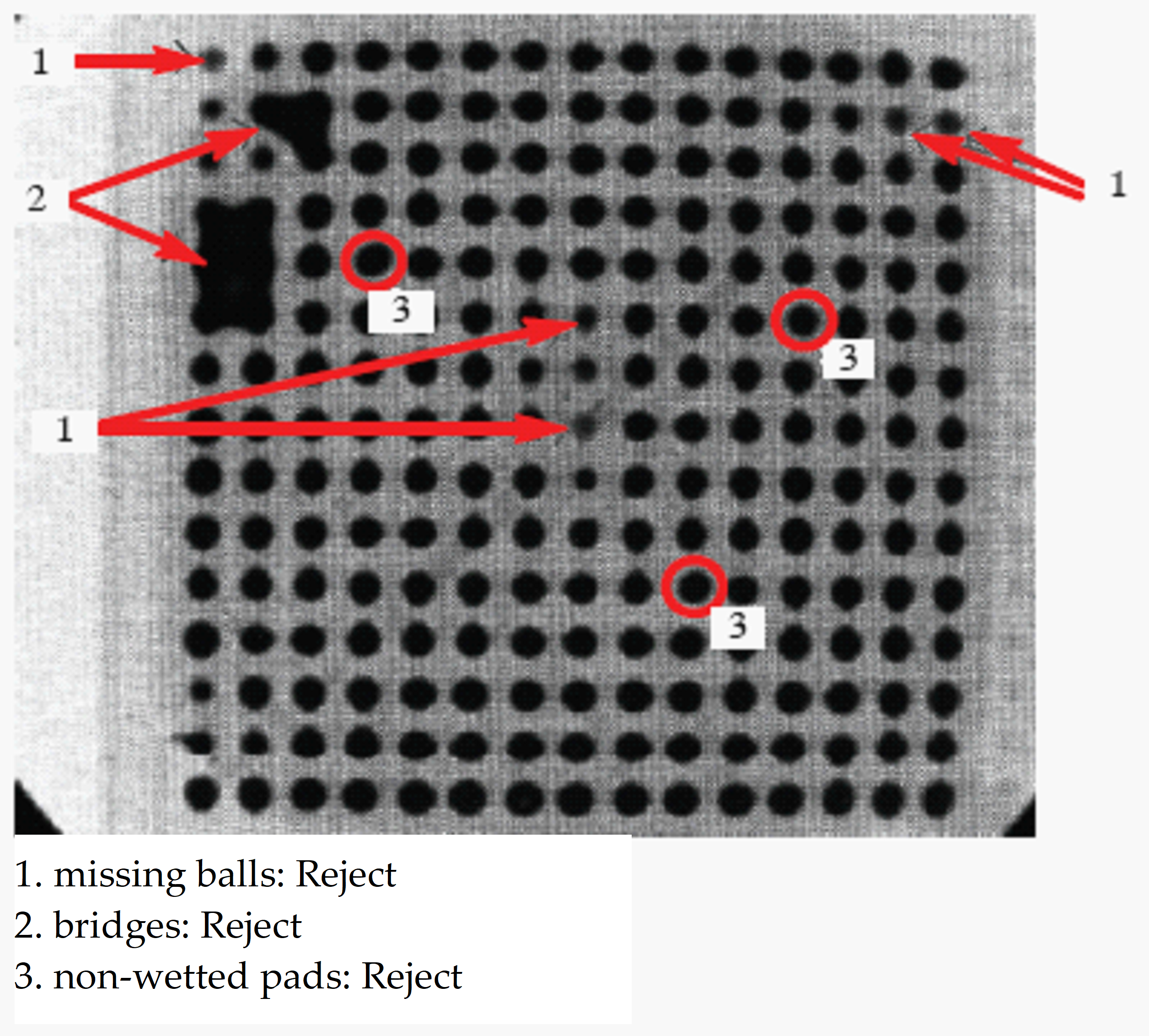 Figure: Perpendicular transmission X-radiograph showing unacceptable defects
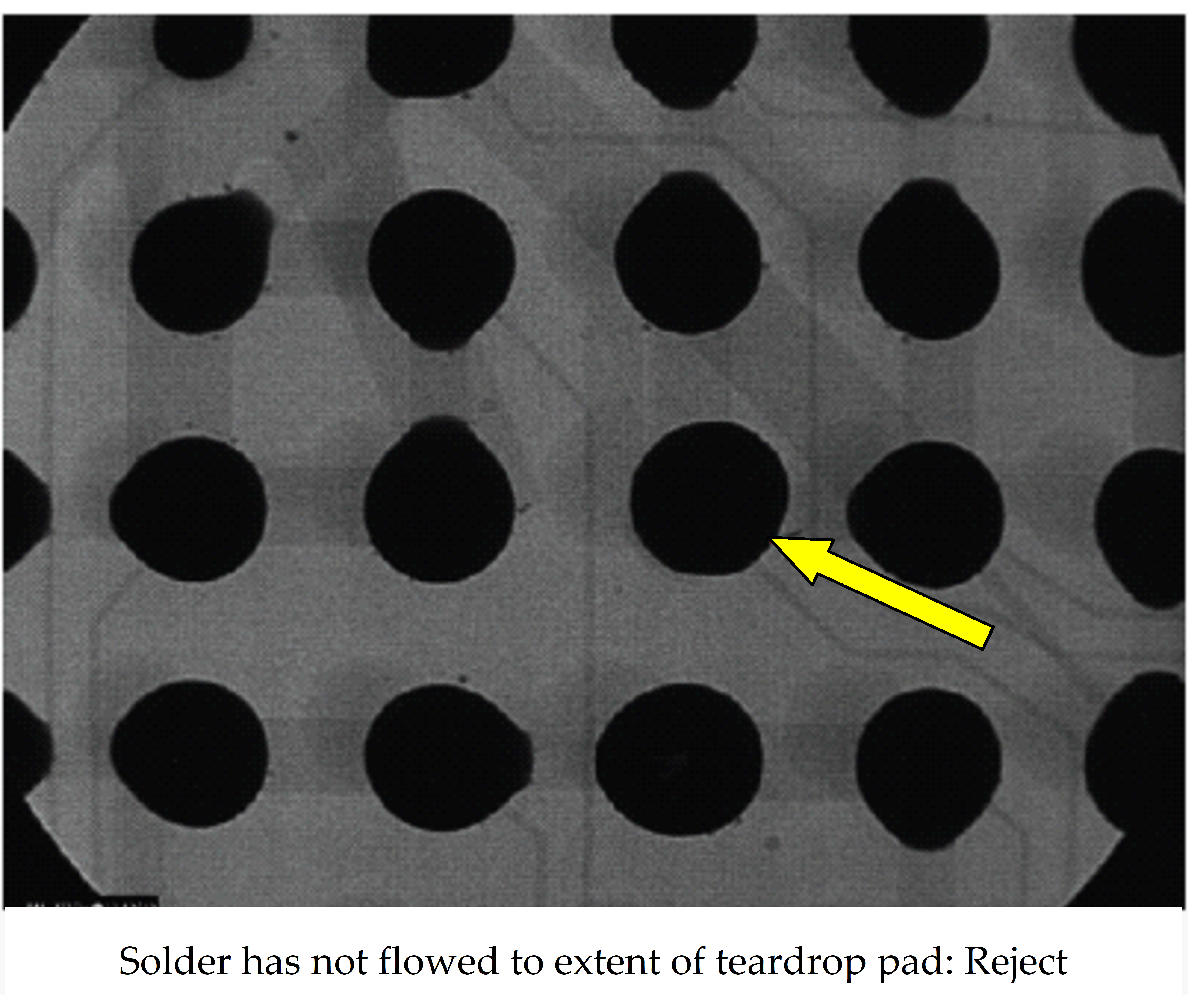 Figure: Perpendicular transmission X-radiograph showing non-wetted footprint
Workmanship illustrations for column grid array devices
: 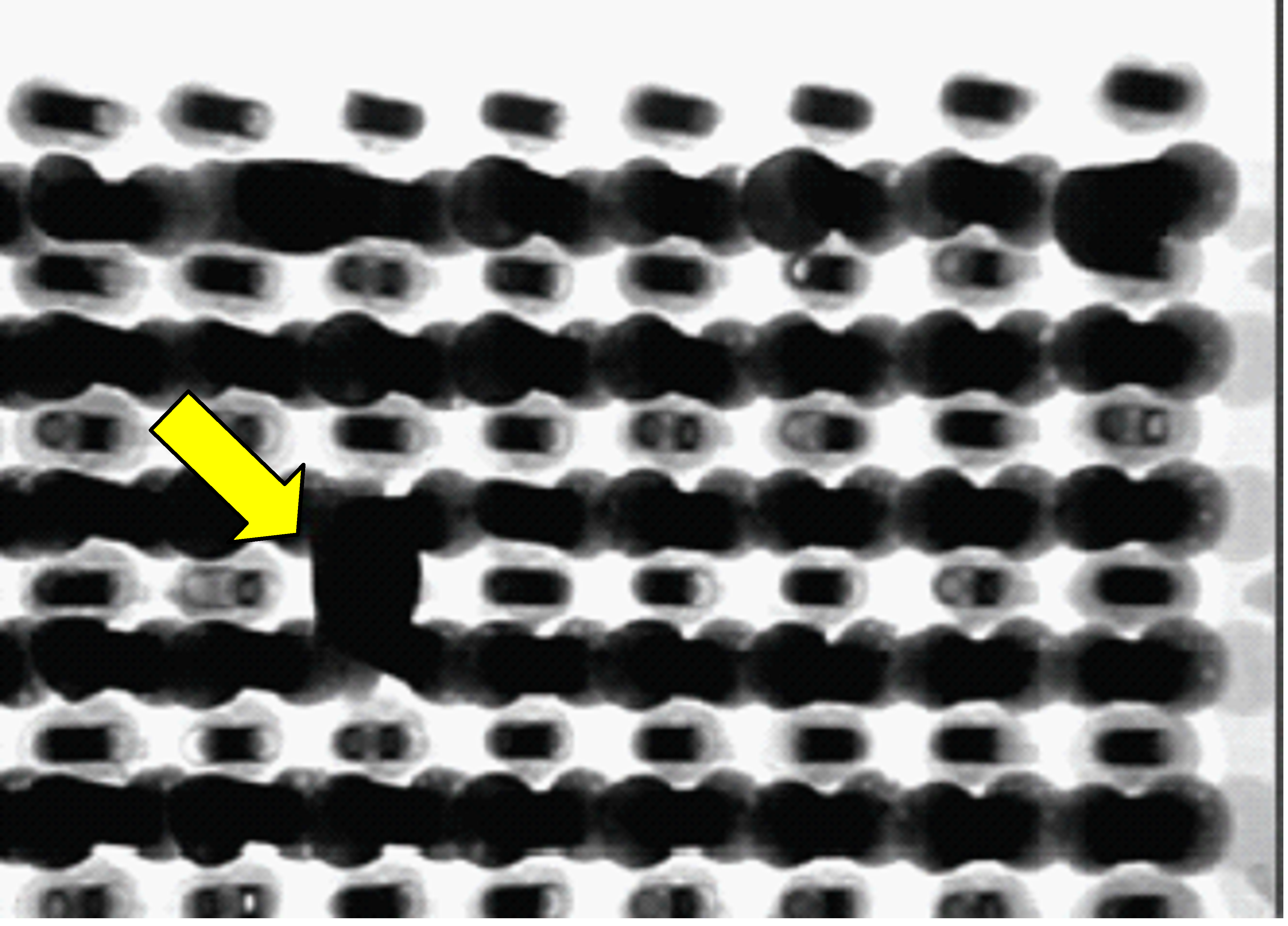
Figure: X-radiograph of CGA mounted on PCB showing solder bridge: Reject
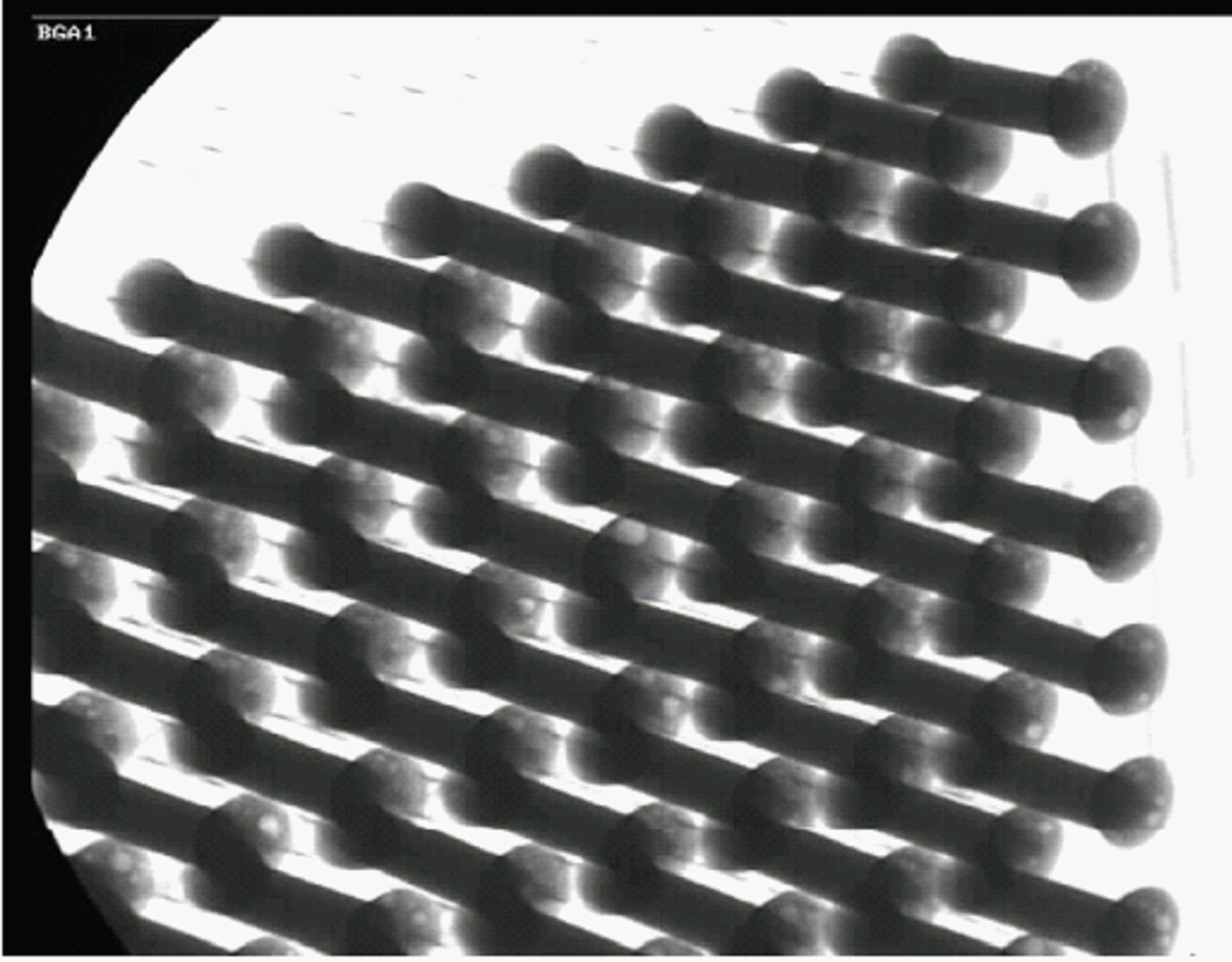 Figure: X-radiograph of CGA showing solder fillets at base of columns: acceptable
ANNEX(informative)Example of an SMT audit report
ECSS-Q-ST-70-61C: SURFACE MOUNT TECHNOLOGY PROCESS AUDIT REPORT
|
SECTION 1 |
COMPANY DETAILS |
||||
|
1. NAME |
|
||||
|
2. ADDRESS |
|
||||
|
3. TEL |
|
||||
|
4. EMAIL |
|
||||
|
5. MANAGING DIRECTOR |
|
||||
|
6. QUALITY MANAGER |
|
||||
|
7. PRODUCTION MANAGER |
|
||||
|
8. SMT CONTACT PERSON |
|
||||
|
9. SMT PRODUCT RANGE AND HISTORY (brief summary) |
|
||||
|
10. Numbers of SMT operators |
|
Design Engineers |
|
QA |
|
ECSS-Q-ST-70-61C Rev 1: SURFACE MOUNT TECHNOLOGY PROCESS AUDIT REPORT
|
SECTION 2 |
QUALITY SYSTEM |
|||||
|
1. QUALITY MANUAL* Reference: |
|
|||||
|
Issue: |
|
|||||
|
Date: |
|
Viewed |
Y N |
|||
|
2. ORGANISATION OF THE QUALITY DEPARTMENT FOR SMT |
|
|||||
|
3. INTERNAL QUALITY AUDIT SYSTEM Reference: |
|
|||||
|
Date of last audit: |
|
|||||
|
Comments: |
|
Viewed |
Y N |
|||
|
4. NON-CONFORMANCE SYSTEM Reference: |
|
|||||
|
|
No. of NCRs in previous 12 months: |
|
No. open at audit date: |
|
Viewed |
Y N |
|
5. CURRENT QUALITY APPROVALS Date of last assessment |
|
|||||
|
6. COMMENT ON COMMITMENT TO ECSS-Q-ST-70-61 |
|
|||||
|
7. REFERENCE TO GENERAL ESA AUDIT & Date |
|
|||||
- Note: Request that a copy of the Contents List of the Quality Manual be appended to this report (See Attachment 1).
ECSS-Q-ST-70-61C Rev.1: SURFACE MOUNT TECHNOLOGY PROCESS AUDIT REPORT
|
SECTION 3 |
PROCESS CONTROL |
|
1. SMT APPROVED (if any) Make reference to an existing list of SMT configurations considered already tested. Identify how the SMT was tested. |
|
|
2. Make reference to the procedures that have the following functions and identify current issue and date: |
|||
|
Process Identification Document |
|
||
|
1. Process instructions |
|
||
|
|
|
Viewed: |
Y N |
|
2. Workmanship acceptance/rejection criteria |
|
||
|
|
|
Viewed: |
Y N |
|
3. Calibration of SMT tooling |
|
||
|
|
Viewed: |
Y N |
|
|
4. Control of limited Shelf life materials |
|
||
|
|
|
Viewed: |
Y N |
|
5. Material procurement control with CofC or CofTest |
|
||
|
|
Viewed: |
Y N |
|
|
3. TRAINING Make reference to the procedure for operator and inspector training. Identify the number of certificated operators and inspectors. |
|
|||
|
|
Viewed: |
Y N |
Certificates viewed: |
Y N |
ECSS-Q-ST-70-61C Rev.1: SURFACE MOUNT TECHNOLOGY PROCESS AUDIT REPORT
|
SECTION 4 |
FACILITIES |
|
CHECK LIST |
|
|
Devices storage and kitting area. |
|
|
Humidity and temperature control |
|
|
ESD protection and control |
|
|
Cleanliness in assembly areas |
|
|
Calibration |
ESD (floor, mat, chair, wrist, solder iron….): |
|
Degolding, pretinning bath: |
|
|
Lead forming: |
|
|
Machine reflow: |
|
|
Solder tip: |
|
|
Repair station: |
|
|
Ovens: |
|
|
Lighting in Lux |
Degolding: |
|
Pretinning: |
|
|
Lead forming: |
|
|
HS Assembly: |
|
|
Stacking, bonding: |
|
|
Conformal coating: |
|
|
PCB drying ovens and procedure |
Unpopulated: |
|
Populated without conformal coating: |
|
|
Populated with conformal coating: |
|
|
Oven |
Baking of naked PCB: |
|
Baking of populated PCB: |
|
|
Curing of adhesive: |
|
|
Curing of conformal coating: |
|
|
Repair prior conformal coating |
|
|
Repair after conformal coating: |
|
|
Bending tools |
|
|
Magnification aids |
Device preparation (degolding, pretinning, lead forming): |
|
After solder paste application: |
|
|
After assembly by machine reflow: |
|
|
During assembly by hand: |
|
|
Final inspection: |
|
|
Degolding bath (250C-280C) |
|
|
Pretinning (210-260C) |
|
|
Solder fluxes (internal and external) used. Flux activity and trademark. |
Degolding, pretinning: |
|
Solder paste: |
|
|
Hand soldering: |
|
|
Cleaning Solvents |
PCB cleaning: |
|
Degolding, pretinning: |
|
|
Soldering by machine reflow: |
|
|
Solder screen |
|
|
Soldering by hand: |
|
|
Prior to bonding, stacking: |
|
|
Prior to conformal coating: |
|
|
Solder alloys (chemical composition, supplier, trademark and associated flux |
-Dispensing: |
|
Screen printing: |
|
|
HS: |
|
|
Solder paste application |
Stencil: |
|
Dispensing: |
|
|
Repair station: |
|
|
Pick and place machine |
|
|
Machine reflow |
|
|
Is the soldering equipment well controlled (temperature-time profile, speed control…). How is the temperature profile controlled on the FM? |
Machine reflow: |
|
Solder Iron: |
|
|
Hand Soldering iron (280C to 340C max) |
|
|
Fume exhaust facilities |
|
|
Repair station |
|
|
Cleaning Equipment |
Machine reflow |
|
Hand soldering: |
|
|
Cleanliness Testing (< 1,6 g/cm2) |
|
|
Stacking, bonding compounds |
|
|
Refrigerators: check expiration dates for adhesives, conformal coatings |
Solder paste: |
|
Adhesive: |
|
|
Conformal coating: |
|
|
Conformal Coating used |
Curing conditions: |
|
Cleanliness in conformal coating facilities |
|
|
Areas for Non-Conforming Items (Quarantine) |
|
|
Laboratories exist for: - Temperature cycling - Vibration - Electrical testing - Microsectioning |
|
|
SMT Assembly Traveller (operator activities, inspector stamps) |
|
END OF SECTION 4ECSS-Q-ST-70-61C: SURFACE MOUNT TECHNOLOGY PROCESS AUDIT REPORT
|
SECTION 5 |
FINAL ASSESSMENT |
An assessment of the surface mount technology line at the following suppliers facility has been undertaken and the following conclusions made:Supplier: Address: THE FACILITIES FOR THE ASSEMBLY OF SURFACE MOUNT TECHNOLOGY (ACCORDING TO ECCS-Q-ST-70-61C AT THE ABOVE SUPPLIER’S SITE ARE CONSIDERED:SUITABLE CONDITIONALLY SUITABLE NOT SUITABLESUMMARY OF FINDINGS/CONDITIONS OF APPROVAL/SUMMARY OF CORRECTIVE ACTIONS NECESSARY:
|
Actions |
Findings |
Due date |
NAME SIGNPROCESS ASSESSMENT CARRIED OUT BY (Approval Authority): IN PRESENCE OF (CONTRACTOR): DATE:Approval Authority: DATE: END OF DOCUMENT
ANNEX(informative)Solder Alloys melting temperatures and choice
Melting temperatures and choice
Table: Guide for choice of solder type
|
Solder type
|
Melting range (°C)
|
Uses
| |
|
|
Solidus
|
Liquidus
|
|
|
63 tin solder (eutectic)
|
183
|
183
|
Soldering printed circuit boards where temperature limitations are critical and in applications with an extremely short melting range. Preferred solder for surface mount components.
|
|
62 tin silver loaded
|
179
|
190
|
Soldering of terminations having silver metallization. This solder composition decreases the scavenging of silver surfaces.
|
|
60 tin solder
|
183
|
188
|
Soldering electrical wire/cable harnesses or terminal connections and for coating or pretinning metals.
|
|
96 tin silver (eutectic)
|
221
|
221
|
Can be used for special applications, such as soldering terminal posts.
|
|
75 indium lead
|
145
|
162
|
Special solder used for low temperature soldering process when soldering gold and gold-plated finishes. Can be used for cryogenic applications.
|
|
70 indium lead
|
165
|
175
|
For use when soldering gold and gold-plated finishes when impractical to degold.
|
|
50 indium lead
|
184
|
210
|
This solder has low gold leaching characteristic.
|
Bibliography
|
ECSS-S-ST-00
|
ECSS system - Description, implementation and general requirements
|
|
ECSS-E-ST-10-03
|
Space engineering - Testing
|
|
ECSS-E-HB-20-05
|
Space engineering - High voltage engineering and design handbook
|
|
ECSS-E-HB-32-25
|
Space engineering - Mechanical shock design and verification handbook
|
|
ANSI/ESD S20.20-2014
|
Protection of Electrical and Electronic Parts, Assemblies and Equipment (Excluding Electrically Initiated Explosive Devices)
|
|
EIA-469 issue E
|
Standard Test Method for Destructive Physical Analysis (DPA)of Ceramic Monolithic CAPA
|
|
EN-IEC 61190-1-2
|
Attachment materials for electronic assembly - Part 1-2: Requirements for soldering pastes for high-quality interconnects in electronics assembly
|
|
EN-IEC 61190-1-3
|
Attachment materials for electronic assembly - Part 1-3: Requirements for electronic grade solder alloys and fluxed and non-fluxed solid solders for electronic soldering applications
|
|
EN-IEC 61340-5-2
|
Electrostatics - Part 5-2: Protection of electronic devices from electrostatic phenomena - User guide
|
|
ESA-TECMSP-MO-018961 (latest release)
|
Devices that have shown anomalies during assembly verification
|
|
ESA-TECMSP-MO-013161 (last release)
|
Procedure for approval of laboratories for microsectioning of electronic assemblies for ESA programmes
|
|
ESA TECMSP-MO-013162 (latest release)
|
Requirements for outsourcing laboratories performing microsectioning of electronic assemblies
|
|
ESA TECMSP-MO-013165
|
ESA recommended microsectioning facilities
|
|
ESA-TECQTM-MO-1931 Issue 3
|
Guideline for the review of Approval status of electronics assembly configurations during MPCB
|
|
MIL-PRF-28861
|
FILTERS: Filters, Radio Interference/Electromagnetic Interference Suppression
|
|
MIL-PRF-39003
|
CAPACITORS: Fixed, Tantalum, Electrolytic (Solid Electrolyte), Polarized, Established Reliability
|
|
MIL-PRF-39010
|
COILS: Coils, Fixed, Radio Frequency, Established Reliability
|
|
MIL-PRF-49470
|
CAPACITORS: Fixed, Ceramic Dielectric, Switch Mode Power Supply
|
|
MIL-PRF-83421
|
CAPACITORS: Fixed, Metallized, Plastic Film Dielectric, Hermetically Sealed, Established Reliability
|