
Space product assurance
High-reliability soldering for surface-mount and mixed technology
Foreword
This Standard is one of the series of ECSS Standards intended to be applied together for the management, engineering and product assurance in space projects and applications. ECSS is a cooperative effort of the European Space Agency, national space agencies and European industry associations for the purpose of developing and maintaining common standards. Requirements in this Standard are defined in terms of what shall be accomplished, rather than in terms of how to organize and perform the necessary work. This allows existing organizational structures and methods to be applied where they are effective, and for the structures and methods to evolve as necessary without rewriting the standards.
This Standard has been prepared by the ECSS Executive Secretariat, reviewed by the Document and Discipline Focal point, and approved by the ECSS Technical Authority.
Disclaimer
ECSS does not provide any warranty whatsoever, whether expressed, implied, or statutory, including, but not limited to, any warranty of merchantability or fitness for a particular purpose or any warranty that the contents of the item are error-free. In no respect shall ECSS incur any liability for any damages, including, but not limited to, direct, indirect, special, or consequential damages arising out of, resulting from, or in any way connected to the use of this Standard, whether or not based upon warranty, business agreement, tort, or otherwise; whether or not injury was sustained by persons or property or otherwise; and whether or not loss was sustained from, or arose out of, the results of, the item, or any services that may be provided by ECSS.
Published by: ESA Requirements and Standards Division
ESTEC, P.O. Box 299,
2200 AG Noordwijk
The Netherlands
Copyright: 2017© by the European Space Agency for the members of ECSS
Change log
|
ECSS-Q-70-38A
|
First issue
|
|
ECSS-Q-70-38A Rev.1
|
Second issue
|
|
ECSS-Q-70-38B
|
Never issued
|
|
ECSS-Q-ST-70-38C
|
Third issue
|
|
ECSS-Q-ST-70-38C Rev.1
|
Third issue, Revision 1
|
Introduction
This Standard prescribes requirements for electrical connections of leadless and leaded surface mounted devices (SMD) on spacecraft and associated equipment, utilising a range of substrate assemblies and employing solder as the interconnection media. The principal types of SMDs can be gathered in the following families:
|
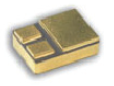
Rectangular and square end-capped or end-metallized device with rectangular body, leadless chip (see 11.5.2)
|

|
|
Cylindrical and square end-capped devices with cylindrical body, leadless chip (see 11.5.4)
|

 |
|
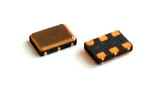
Bottom terminated chip device (see 11.5.3)
|

  |
|
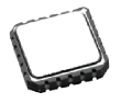
Castellated chip carrier device (see 11.5.5)
|
|
|
Flat pack and gull-wing leaded device with round, rectangular , ribbon leads (see 11.5.6)
|
|
|
Moulded magnetics (see 11.5.13)
|
 |
|
“J” leaded device (see 11.5.7)
|
|
|
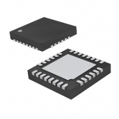
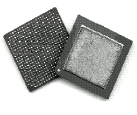
Area array devices (AAD) (see 11.5.8)
|
|
|
Devices with ribbon terminals without stress relief (flat lug leads) (see 11.5.9)
|
|
|
Device with Inward formed L-shaped leads (see 11.5.10)
|

|
|
Stacked modules devices with leads protruding vertically from bottom (see 11.5.11)
|
|
|
Leaded device with plane termination (see 11.5.12)
|
|
Scope
This Standard defines the technical requirements and quality assurance provisions for the manufacture and verification of high-reliability electronic circuits based on surface mounted device (SMD) and mixed technology.
The Standard defines acceptance and rejection criteria for high-reliability manufacture of surface-mount and mixed-technology circuit assemblies intended to withstand normal terrestrial conditions and the vibrational gloads and environment imposed by space flight.
The proper tools, correct materials, design and workmanship are covered by this document. Workmanship standards are included to permit discrimination between proper and improper work.
The assembly of leaded devices to through-hole terminations and general soldering principles are covered in ECSS-Q-ST-70-08.
Requirements related to printed circuit boards are contained in ECSS-Q-ST-7010, ECSS-Q-ST-70-11 and ECSS-Q-ST-70-12 .
The mounting and supporting of devices, terminals and conductors prescribed herein applies to assemblies at PCB level designed to continuously operate over the mission within the temperature limits of -55 C to +85 C.
For temperatures outside this normal range, special design, verification and qualification testing is performed to ensure the necessary environmental survival capability.
Special thermal heat sinks are applied to devices having high thermal dissipation (e.g. junction temperatures of 110 C, power transistors) in order to ensure that solder joints do not exceed 85 C.
Verification of SMD assembly processes is made on test vehicles (surface mount verification samples). Temperature cycling ensures the operational lifetime for spacecraft. However, mechanical testing only indicates SMD reliability as it is unlikely that the test vehicle represents every flight configuration.
This Standard does not cover the qualification and acceptance of the EQM and FM equipment with surface-mount and mixed-technology.
The qualification and acceptance tests of equipment manufactured in accordance with this Standard are covered by ECSS-E-ST-10-03.
This standard may be tailored for the specific characteristics and constraints of a space project, in accordance with ECSS-S-ST-00.
Normative references
The following normative documents contain provisions which, through reference in this text, constitute provisions of this ECSS Standard. For dated references, subsequent amendments to, or revisions of any of these publications do not apply. However, parties to agreements based on this ECSS Standard are encouraged to investigate the possibility of applying the most recent editions of the normative documents indicated below. For undated references the latest edition of the publication referred to applies.
|
ECSS-S-ST-00-01
|
ECSS system — Glossary of terms
|
|
ECSSMST40
|
Space project management — Configuration and information management
|
|
ECSSQST10-09
|
Space product assurance — Nonconformance control system
|
|
ECSSQST20
|
Space product assurance — Quality assurance
|
|
ECSSQST60
|
Space product assurance — Electrical, electronic and electromechanical (EEE) components
|
|
ECSSQST60-05
|
Space product assurance — Generic requirements for hybrids
|
|
ECSS-Q-ST-60-13
|
Space product assurance - Commercial electrical, electronic and electromechanical (EEE) components
|
|
ECSSQST70
|
Space product assurance — Materials, mechanical parts and processes
|
|
ECSSQST70-01
|
Space product assurance — Cleanliness and contamination control
|
|
ECSSQST70-02
|
Space product assurance — Thermal vacuum outgassing test for the screening of space materials
|
|
ECSSQST70-08
|
Space product assurance — Manual soldering of high–reliability electrical connections
|
|
ECSSQST70-10
|
Space product assurance — Qualification of printed circuit boards
|
|
ECSSQST70-11
|
Space product assurance — Procurement of printed circuit boards
|
|
ECSS-Q-ST-70-12
|
Space product assurance — Design rules for printed circuit boards
|
|
ECSS-Q-ST-70-28
|
Space product assurance — Repair and modification of printed circuit board assemblies for space use.
|
|
ECSSQST70-71
|
Space product assurance —Materials processes and their data selection
|
|
MIL-STD-883 Method 2009
|
Test Method Standard, Microcircuits
|
|
IPC-TM-650: 2.6.3.3 Issue 2004
|
Test methods manual. Surface Insulation Resistance, Fluxes
|
Terms, definitions and abbreviated terms
Terms from other standards
For the purpose of this Standard, the terms and definitions from ECSSSST0001 apply.
For the purpose of this Standard, the terms and definitions from ECSS-Q-ST-60 apply, in particular for the following term(s):
commercial component
For the purpose of this Standard, the terms and definitions from ECSS-Q-ST-70-28 apply, in particular for the following term(s):
repair
rework
Terms specific to the present standard
approval authority
entity that reviews and accepts the verification programme, evaluating the test results and grants the final approval
bonding
application process of adhesive under a SMD package for mechanical or thermal purpose where adhesive joint is not visible
co-planarity
maximum distance between lowest and highest termination when device rests on flat surface
collective assembled devices
set of components that are soldered to PCB in one operation
critical zone
area in the solder joint in which the existence and magnitude of cracks is subject to acceptance or rejection
device
package, component or part
dynamic wave soldering machine
system that achieves wave soldering and which consists of stations for fluxing, preheating, and soldering by means of a conveyer
electrical clearance
spacing between non-common electrical conductors on external layers of a printed circuit board assembly
The distance between conductors depends on the design voltage and DC or AC peaks. Any violation of minimum electrical clearance as a result of a nonconformance is a defect condition.
reprocessing
preparatory operation done on a device prior to assembly
Retinning, degolding, lead forming are examples of reprocessing.
scavenging (leaching)
basis metal or metallization partly or wholly dissolved in melted solder during a soldering operation
selective plating
tin-lead plated solder footprints connected to gold plated copper tracks
It is usually related to RF circuits.
sensitive devices
device prone to have cracks in solder joint exceeding 75 % of acceptance criteria or showing nonconformance outside the component manufacturer limit
- 1 ESA list of sensitive devices is published on ESCIES for information, see www.escies.org.
- 2 Each company maintains its own list of sensitive devices in the PID.
solder balling (solder balls)
numerous spheres of solder having not melted in with the joint form and being scattered around the joint area normally attached by flux residues
Can be caused by incorrect preheating or poor quality solder.
stacking
application process of adhesive at extremities of a SMD package for mechanical purpose where adhesive joint is partially visible
solder stand-off
thickness of solder between the underside of the device termination and the surface of the PCB footprint
test vehicle
substrate assembled with Surface Mounted Devices subjected to a verification programme
tombstoning
chip devices lifting off one of their two terminal footprints causing the chip to stand up like a tombstone
Normally caused by:
- bad design where one footprint reaches solder reflow temperature before the other;
- different quantities of solder paste on each footprint;
- different solderability of one footprint or one termination with respect to the other.
underfill
encapsulant material deposited between a device and substrate
Abbreviated terms
For the purpose of this Standard, the abbreviated terms from ECSSSST0001 and the following apply:
|
Abbreviation
|
Meaning
|
|
AAD
|
area array device
|
|
BGA
|
ball grid array
|
|
CBGA
|
ceramic ball grid array
|
|
CCGA
|
ceramic column grid array
|
|
CGA
|
column grid array
|
|
CLCC
|
ceramic leaded chip carrier
|
|
CTE
|
coefficient of thermal expansion
|
|
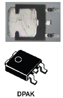
DPAK
|
diode package
|
|
DRD
|
document requirement definition
|
|
FM
|
flight model or flight hardware
|
|
FP
|
flat pack package
|
|
JEDEC
|
Joint Electron Device Engineering Council
|
|
LCCC
|
leadless ceramic chip carrier
|
|
MELF
|
metal electrode face bonded
|
|
MIP
|
mandatory inspection point
|
|
PCB
|
printed circuit board
|
|
PLCC
|
plastic leaded chip carrier
|
|
PID
|
process identification document
|
|
QFN
|
quad flat pack no leads
|
|
QFP
|
quad flat pack
|
|
r.m.s.
|
root-mean-square
|
|
SIR
|
surface insulation resistance
|
|
SMD
|
surface mounted device
|
|
SMT
|
surface-mount technology
|
|
SO
|
small outline
|
|
SOD
|
small outline device
|
|
SOT
|
small outline transistor
|
|
SOP
|
small outline package
|
|
TO
|
transistor outline
|
|
TSOP
|
thin small outline package
|
Nomenclature
Formal verbs
The following nomenclature apply throughout this document:The word “shall” is used in this document to express requirements. All the requirements are expressed with the word “shall”.
The word “should” is used in this document to express recommendations. All the recommendations are expressed with the word “should”.
It is expected that, during tailoring, all the recommendations in this standard are either converted into requirements or tailored out.
The words “may” and “need not” are used in this document to express positive and negative permissions respectively. All the positive permissions are expressed with the word “may”. All the negative permissions are expressed with the words “need not”.
The word “can” is used in this document to express capabilities or possibilities, and therefore, if not accompanied by one of the previous words, it implies descriptive text.
In ECSS “may” and “can” have a complete different meaning: “may” is normative (permission) and “can” is descriptive.
The present and past tense are used in this document to express statement of fact, and therefore they imply descriptive text.
Principles of reliable soldered connections
The following are the general principles to ensure reliable soldered connections:
Reliable soldered connections are the result of proper design, control of tools, materials, processes and work environments, and workmanship performed in accordance to verified and approved procedures, inspection control and precautions.
The basic design concepts to ensure reliable connections and to avoid solder joint failure are as follows:
Stress relief is an inherent part of the design, which reduces detrimental thermal and mechanical stresses on the solder connections.
Where adequate stress relief is not possible materials are so selected that the mismatch of thermal expansion coefficients is a minimum at the constraint points in the device mounting configuration.
The assembled substrates are designed to allow easy inspection.
Since only the outer row of solder joints to area array packages can be visually inspected, inner rows are inspected using X-ray techniques. To facilitate X-ray inspection of the solder joints to BGAs, the solder footprints can have a teardrop design.
Circuit designs for area array devices, (e.g. BGA, CGA) have clearance around the perimeter of these packages to ensure that reflow nozzles can perform rework or repair operations (see ECSSQST70-28). The clearance depends on the equipment used for reworking and the height of adjacent components.
Unpopulated areas on the underside of the substrate assist indirect heating for removal of these packages.
Soldering to gold using tin-lead alloy can cause failure.
Process identification document (PID)
General
Purpose
The purpose of the PID is to ensure that a precise reference is established for the assembly processes approved in accordance with this Standard.
The PID provides a standard reference against which any anomalies occurring after the approval can be examined and resolved.
Document preparation
The supplier shall prepare the PID in conformance with DRD from Annex F.
The supplier shall provide a draft PID prior to any start of verification to the Approval Authority.
The first issue of the PID shall fully comply to this standard.
For supplier, already approved on the basis of reliable tests results which supported the approval of any deviation finally recorded in the PID, then the PID may supersede the corresponding requirements from this standard.
<<deleted>>
<<deleted>>
<<deleted>>
Approval
The PID shall be submitted to the Approval Authority for approval.
The approval can be achieved by PID signature or minutes of meeting being signed by the Approval Authority.
<<deleted>>
SMT contact person
The supplier shall appoint a contact person for SMT topics.
<<deleted>>
<<deleted>>
<<deleted>>
<<deleted>>
<<deleted>>
<<deleted>>
Process identification document updating
The PID shall be managed in accordance with ECSS-M-ST-40.
A PID shall represent the current verified manufacturing processes and production controls.
Any proposed change to the PID shall be agreed by the Approval Authority.
<<deleted>>
The supplier shall initiate a review of the PID, the SMT summary table and the relevant applicable documents at least every two years for agreement by the Approval Authority.
Preparatory conditions
Calibration
The supplier shall maintain records of tool calibration and verification.
Requirements from clause 5.1 from ECSSQST7008 shall apply for “Calibration”.
Facility cleanliness
Requirements from clause 5.2 from ECSSQST7008 shall apply for “Facility cleanliness”.
Environmental conditions
Requirements from clause 5.3 from ECSSQST7008 shall apply for “Environmental conditions”.
Precautions against static charges
Requirements from clause 5.5 from ECSSQST7008 shall apply for “Precautions against static charges”.
Lighting requirements
Requirements from clause 5.4 from ECSSQST7008 shall apply for “Lighting requirements”.
Equipment and tools
Brushes
Requirements from clause 5.6.2 from ECSSQST7008 shall apply for "Brushes".
Cutters and Pliers
Requirements from clause 5.6.3 from ECSSQST7008, shall apply for "Cutters and Pliers".
Bending tools
Requirements from clause 5.6.4 from ECSSQST7008 shall apply for "Bending tools".
Clinching tools
Requirements from clause 5.6.5 from ECSSQST7008 shall apply "Clinching tools".
Insulation strippers
Requirements from clause 5.6.6 from ECSSQST7008 shall apply for "Insulation strippers".
Soldering tools
Requirements from clause 5.6.8 from ECSSQST7008 shall apply for "Soldering tools".
Soldering irons and resistance soldering equipment
Requirements from clause 5.6.7 from ECSSQST7008 shall apply for “Soldering irons and resistance soldering equipment”.
For surface mounted devices, the soldering tip shall not exceed 340 C.
Based on the device manufacturer’s recommendations, solder iron can be substituted by applying, for instance, hot air in order to avoid thermal shock.
<<deleted>>
<<deleted>>
Solder baths for degolding and pretinning
Requirements from clause 7.2.3.2.2 from ECSSQST7008 shall apply for "Solder baths" for degolding and pretinning.
Soldering machines and equipment
General
Machines and equipment used to solder surface mount devices shall either be a type incorporating dynamic single or dual solder wave, or be of the solder reflow type.
The soldering machine shall be grounded in order to avoid electrostatic discharge.
The supplier shall ensure that the soldering conditions do not exceed the values given by the individual device data sheets
Examples of soldering conditions include. maximum temperature to avoid internal melting, removal of marking ink, degradation of encapsulating plastic.
Temperature and time profiles for assembly shall be identified by the supplier and approved by the Approval Authority.
The supplier shall identify changes and implement a verification programme in compliance with the requirements from clause 14.13.
The supplier shall demonstrate the reproducibility of their reflow processes.
Dynamic wave-solder machines
Dynamic soldering machines shall be of automatic type and of a design offering the following:
- Controllable preheating to drive off volatile solvents and to avoid thermal shock damage to the PCB and device packages.
- The capacity to maintain the solder temperature at the printed circuit board assembly to within 5 C of the established bath temperature throughout the duration of any continuous soldering run when measured 3,0 mm below the surface of the wave.
- A wave system that limits shadowing and allows solder fillet formation.
- Carriers made from a material that cannot contaminate, degrade or damage the printed circuit board or substrate nor transmit vibrations or shock stress from the conveyors to a degree permitting physical, functional or electrostatic damage to devices, board or substrate during transport through preheating, soldering and cooling stages.
- An extraction system, either integral or separate, conforming to the requirements of clauses 6.2a and 6.3a.
Condensation (vapour phase) reflow machines
Condensation reflow machines shall conform to the following requirements:
- Not transmit a movement or vibration into the assemblies being soldered that result in misalignment of devices or disturbed solder joints.
- Be capable of preheating an assembly with solder paste to the temperature recommended by the solder paste manufacturer prior to soldering.
- Use a reflow fluid whose boiling point is a minimum of 12 C above the melting point of the solder being used.
- Maintain the preselected temperature to within 5 C in the reflow zone during soldering.
- Include an extraction system that conforms to requirements 6.2a and 6.3a.
Hot gas reflow machines
Hot gas reflow machines shall conform to the following requirements:
- Does not transmit movement or vibration to the assemblies being soldered which result in misalignment of devices or disturbed solder joints.
- Preheats an assembly with solder paste to the temperature recommended by the solder paste manufacturer prior to soldering.
- <<deleted>>
- Prevents the reflow of adjacent devices.
- Maintains the preselected reflow temperature within 5 C as measured at the substrate surface.
<<deleted>>
<<deleted>>
Convection and radiation reflow systems
Convection and radiation reflow machines shall be of design such that the system meets the following requirements:
- Provides a controlled temperature profile and does not transmit movement or vibration into the assembly being soldered.
- Preheats an assembly with solder paste to the temperature recommended by the solder paste manufacturer prior to soldering.
- Heats the area of the assembly to be soldered using focused or unfocussed energy, to a preselected temperature that is a minimum of 12 C above the melting point of the solder being used as measured at laminate or substrate surface.
- Maintains the preselected temperature to within ±5 C in the reflow zone during soldering.
Other equipment for reflow soldering
Other solder reflow systems may be approved for use by the Approval Authority, if compliance with clauses 6.7.1 to 6.7.6 is demonstrated.
Ancillary equipment
General
Equipment shall not generate, induce or transmit electrostatic charges to devices being placed.
The supplier shall demonstrate the reproducibility of their SMT processes.
Solder deposition equipment
Equipment used to deposit solder pastes shall be of a screening, stencilling, dispensing, roller coating, dotting or jet printing type.
Equipment shall apply pastes of a viscosity and quantity such that the positioned device is retained on the board before and during soldering operations, ensuring self-centring and solder fillet formation.
Equipment used to apply solder preforms shall ensure alignment of the preform with the land or device lead and termination.
Automatic device placement equipment
Automatic or computer controlled equipment used for device placement shall be of the coordinate-driven pick-and-place type or of the robotic type.
The placement equipment used shall be of a type that:
- prevents device or board damages
- indexes devices with respect to the circuit
- aligns the device leads or castellations with the board terminal areas.
<<deleted>>
<<deleted>>
Cleanliness testing equipment
Requirements from clause 11.3.1 from ECSSQST7008 shall apply for “Cleanliness testing”.
Magnification aids
Clause 13.1 shall apply.
X-ray inspection equipment
The maximum dose during X-Rays inspection shall be less than 5 % of the eligible dose of the most sensitive component according to its specification.
X-ray equipment shall be calibrated in order to evaluate the total dose received by the devices during the inspection.
In order to minimize the dose given to the device, it is good practice to:
- Record the total dose received.
- Use off-line image analysis as much as possible.
- Use filters, optimizing the direction of the X-ray beam and masking sensitive areas.
The resolution of the X-ray equipment shall be able to detect solder balls having a diameter of 0,03 mm.
The sensitivity shall be demonstrated by means of actual 0,03 mm diameter solder balls, stuck to adhesive tape, attached to the multilayer board assembly being inspected.
<<deleted>>
Metallographic equipment
The metallographic equipment shall enable cross-sectioning and polishing of the moulded solder interconnections.
Material selection
General
Material selection shall be performed in accordance with ECSSQST7071 and ECSS-Q-ST-70.
Solder
Form
Solder paste, ribbon, wire and preforms shall be used provided that the alloy and flux meet the requirements in clause 7.2.2.
Alloy for use in solder baths shall be supplied as ingots (without flux) and be compliant with requirements from clause 7.2.2.
Composition
The solder alloy shall have a composition specified in Table 71.
- 1 Use EN 61190-1-3 for solder and EN 61190-1-1 for flux, EN 61190-1-2 for solder paste.
- 2 The solder alloy used depends upon the application. See Annex E.2 for Guide for choice of solder type.
Solder paste
<<deleted>>
The metal purity shall be as specified in Table 71.
Table 71: Chemical composition of spacecraft solders
|
ESA designation |
Sn |
Pb |
In |
Sb |
Ag |
Bi |
Cu |
Fe |
Zn |
Al |
As |
Cd |
Other |
|
min % - max % |
max % |
min % – max % |
max % |
min % – max % |
max % |
max % |
max % |
max % |
max % |
max % |
max % |
max % |
|
|
63 tin solder |
62,5-63,5 |
remainder |
- |
0,05 |
- |
0,10 |
0,05 |
0,02 |
0,001 |
0,001 |
0,03 |
0,002 |
0,08 |
|
62 tin silver loaded |
61,5-62,5 |
remainder |
- |
0,05 |
1,8-2,2 |
0,10 |
0,05 |
0,02 |
0,001 |
0,001 |
0,03 |
0,002 |
0,08 |
|
60 tin solder |
59,5-61,5 |
remainder |
- |
0,05 |
- |
0,10 |
0,05 |
0,02 |
0,001 |
0,001 |
0,03 |
0,002 |
0,08 |
|
96 tin solder |
remain |
0,10 |
- |
0,05 |
3,5-4,0 |
0,10 |
0,05 |
0,02 |
0,001 |
0,001 |
0,03 |
0,002 |
0,08 |
|
75 indium lead |
max 0,25 |
remainder |
74,0-76,0 |
0,05 |
- |
0,10 |
0,05 |
0,02 |
0,001 |
0,001 |
0,03 |
0,002 |
0,08 |
|
70 indium lead |
0,00-0,10 |
remainder |
69,3-70,7 |
0,05 |
- |
0,10 |
0,05 |
0,02 |
0,001 |
0,001 |
0,03 |
0,002 |
0,08 |
|
50 indium lead |
0,00-0,10 |
remainder |
49,5-50,5 |
0,05 |
- |
0,10 |
0,05 |
0,02 |
0,001 |
0,001 |
0,03 |
0,002 |
0,08 |
|
10 tin lead |
9,0-10,5 |
remainder |
- |
0,05 |
- |
0,10 |
0,05 |
0,02 |
0,001 |
0,001 |
0,03 |
0,002 |
0,08 |
Maintenance of paste purity
When purchased premixed or mixed in house, the purity of solder paste shall be maintained.
Manufacturers’ instructions shall be applied for the handling and storage of containers of solder paste purchased premixed.
Refrigerated solder paste shall reach room temperature before opening the container.
Neither paste purchased premixed nor paste mixed in-house shall be used if the use-by date or shelf life recommended by the manufacturer of the paste or paste constituents has expired.
When the solder paste’s shelf life has expired it shall not be used unless:
- relifing is performed
- tests that include visual inspection and viscosity measurements (according to the manufacturer’s recommendations) are passed successfully.
When relifing is performed, and the material passes the specified tests, the new shelf life shall be half the initial shelf life.
Tools used for removing solder paste from the container shall not contaminate the paste dispensed or that remaining within.
Flux
Rosin based flux
Requirements from clause 6.3.1 from ECSSQST7008 shall apply for "Rosin based flux".
Corrosive acid flux
Requirements from clause 6.3.2 from ECSSQST7008 shall apply for "INH1 Corrosive acid flux".
Flux controls for wave-soldering equipment
A controlled method shall be established and implemented for wave-soldering machines such that the flux is not contaminated with remaining residues from previous non-space works.
Solvents
Requirements from clause 6.4 from ECSSQST7008 shall apply for "Solvents".
Flexible insulation materials
Requirements from clause 6.5 from ECSSQST7008 shall apply for "Flexible insulation materials".
Terminals
Requirements from clause 6.6 from ECSSQST7008 shall apply for "Terminals".
Wires
Requirements from clause 6.7 from ECSSQST7008 shall apply for "Wires".
Printed circuit substrates
Printed Circuit Boards shall be designed in conformance with the requirements of clause 14 of ECSSQST70-12.
Printed Circuit Boards shall be made of materials and manufactured in conformance with the requirements of clause 9 of ECSSQST70-10.
Printed Circuit Boards shall be procured in conformance with the requirements of clauses 5 and 6 of ECSSQST70-11.
<<deleted>>
<<deleted>>
<<deleted>>
<<deleted>>
Table 72: <<deleted>>
<<deleted>>
<<deleted>>
<<deleted>>
<<deleted>>
<<deleted>>
<<deleted>>
<<deleted>>
<<deleted>>
<<deleted>>
<<deleted>>
Devices
General
Devices and their finishes shall be selected from those approved in conformance with requirements from clauses 4, 5 and 6 of ECSSQST60, for “manufacturer and component evaluation” and “Procurement control”.
<<deleted>>
Solder may be applied to the terminations by hot dipping or by electroplating from a solution.
Devices with terminations finished by electroplating can impact the device wetting.
<<deleted>>
The incoming inspection of each device batch shall include the verification by test of the termination composition, to avoid assembly of pure tin finish, in accordance with requirement 4.3.7b from ECSS-Q-ST-60.
Pure tin finish with more than 97 % purity shall not be used.
This is due to the possibility of whisker growth and transformation to grey tin powder at low temperatures.
<<deleted>>
<<deleted>>
Devices shall be capable of withstanding cleaning processes currently used in space projects.
Parts with silver palladium finish shall not be used.
Reprocessing shall not damage the device.
Reprocessing of ceramic chip capacitors is advised to be avoided due to potential crack formation.
If devices initially designed for insertion-mount application are used for surface mounting, they shall be of a type that can be surface-mount adapted.
The adaptation specified in the requirement 7.9.1l shall not functionally or physically degrade the device or the substrate to which the adapted device is to be attached.
Connectors shall be of a configuration incorporating either male or female quick-disconnect contacts and stress relief provision for the soldered connection of each individual contact when such connections are completed.
Type II chip ceramic capacitors shall not be reworked.
<<deleted>>
<<deleted>>
<<deleted>>
<<deleted>>
Moisture sensitive devices
Moisture sensitive devices shall be stored and handled in conformance with the device manufacturer’s recommendations. .
Many types of plastic encapsulated devices, particularly some plastic BGAs, are moisture sensitive.
When moisture sensitive devices are used, bakeout shall be performed in accordance with clause 8.5b.
<<deleted>>
<<deleted, modified and moved to 7.9.1l>>
<<deleted, modified and moved to 7.9.1m>>
<<deleted>>
<<deleted>>
<<deleted and moved to 7.9.1n>>
Adhesives, encapsulants and conformal coatings
Adhesives shall be dispensable, non-stringing, and have a reproducible dot profile after application.
Adhesives, encapsulants and conformal coating shall be non-corrosive to devices and substrates.
The uncured strength shall be capable of holding devices during handling prior to curing.
Adhesives, encapsulants and conformal coatings shall conform to the outgassing requirements of ECSSQST70-02.
Adhesives, encapsulants and conformal coatings shall have no adverse effects upon materials used on the substrate, or devices attached thereon.
The effects of some conformal coatings on the reliability of mounted SMDs are described in ESA SP-1173.
Adhesives, encapsulants and conformal coatings shall be selected based on their thermal conductivity and dielectric properties.
Some thermally conductive adhesives used to dissipate Joule heating are listed in ESA STM-265 “Evaluation of Thermally Conductive Adhesives as Stacking Compounds during the Assembly of Spacecraft Electronics”.
The capability of the adhesives to meet their requirements shall be demonstrated by means of a verification programme in conformance with clause 14.
<<deleted>>
Stress relief of device leads shall not be negated by the encapsulants or conformal coatings.
- 1 This is particularly important at low service temperatures.
- 2 The coefficient of expansion, glass transition temperature and modulus of adhesives used under devices for thermal reasons, for achieving stand-off heights or mechanical support during vibration, can be considered to ensure that the additional stress put on the solder joints does not degrade the solder joint reliability.
Adhesive shall not be in contact with terminal of component.
Bonding shall not be performed on fused tin lead unless the tin lead surface is limited to < 25 % by area of the bonding surface and demonstrated by verification as specified in clause 14.
Spread of bonding material onto surrounding areas shall not be accepted unless it does not reduce the volume of the initial bonding joint.
Bonding material shall not be in contact to surrounding devices.
Bonding with epoxy adhesive directly to glass bodied devices shall not be used.
It is good practice to use a sleeve between glass and the epoxy adhesive.
Preparation for soldering
Preparation of devices and terminals
Preparation of wires and terminals
Requirements from clause 7.2 from ECSSQST7008, clause “Preparation of conductors, terminals and solder cups” shall apply.
Preparation of surfaces to be soldered
Requirements from clause 7.2.2 from ECSSQST7008, clause “Surfaces to be soldered” shall apply.
Degolding and pretinning of conductors
Requirements from clauses 7.2.3 and 7.2.4 from ECSSQST7008 shall apply for "Degolding and pretinning of conductors".
Alloying of pure tin finish
<<deleted>>
Pure tin device terminations shall be pretinned with full tin lead solder coverage.
Pure tin device terminations shall be in compliance with requirements from clauses 7.2.4 and 7.2.6 of ECSS-Q-ST-70-08 and requirement 8.1a from ECSS-Q-ST-60-13.
- 1 Pure tin terminations can be dipped into liquid solder as described in ECSSQST7008, clause 7.2.6 in order to replace the tin with tin-lead alloy.
- 2 Reprocessing of ceramic chip capacitors is not recommended due to potential crack formation.
The reprocessing process shall be verified by micro sectioning and SEM/EDX with respect to alloying and full coverage.
Preparation of solder bit
Requirements from clause 7.3 from ECSSQST7008 shall apply for "Preparation of solder bit".
Handling
Requirements from clause 7.5 from ECSSQST7008 shall apply for "Handling".
Storage
Requirements from clause 7.6 from ECSSQST7008 shall apply for "Storage".
Baking of PCBs and moisture sensitive devices
<<deleted>>
Baking of moisture sensitive devices shall be implemented before any reprocessing or assembly process in conformance with JEDEC classification.
This is to counteract the “popcorn” effect in soldering using oven or vapour phase reflow techniques.
Baking times and temperatures, for moisture sensitive devices, shall be in compliance with manufacturer recommendations and baking times as specified in J-STD-033 and documented.
- 1 Typical baking conditions are from 6 h to 24 h at 125 C depending on the JEDEC classification, except for devices delivered in reels for which a lower temperature and longer time are used.
- 2 It is good practice to store devices under nitrogen, dry air (20 % RH maximum) or partial vacuum.
Baking of unpopulated PCBs should be made as a minimum of 8 hours at 120 °C.
Baking of populated PCBs shall be performed when the PCB has been kept under clean room conditions for more than 72 hours.
Storage of PCBs in dry cabinet interrupts the accumulated baking time.
Baking of populated PCB shall be made at a temperature which does not degrade the devices or assembly.
To limit the bake out operation, which can induce later failure, the PCB can be stored in dry environment after the baking.
Mounting of devices prior to soldering
General requirements
Requirements from clause 8.1 from ECSSQST7008, “Mounting of components – General” shall apply.
Lead bending and cutting requirements
Requirements from clause 8.2 from ECSSQST7008, clause “Lead bending requirements” shall apply.
Mounting of terminals to PCBs
Requirements from clause 8.3 from ECSSQST7008 shall apply for "Mounting of terminals to PCBs".
Lead attachment to through holes
Requirements from clause 8.4 from ECSSQST7008 shall apply for "Lead attachment to through holes".
Mounting of devices to terminals
Requirements from clause 8.5 from ECSSQST7008 shall apply for "Mounting of components to terminals".
Mounting of through hole connectors to PCBs
Requirements from clause 8.6 from ECSSQST7008 shall apply for "Mounting of through hole connectors to PCBs".
Surface mount requirements
General
Devices to be mounted shall be designed for, and be capable of withstanding the soldering temperatures of the particular process being used for fabrication of the assembly.
Surface mounted devices can be mounted on either one side or both sides of a printed circuit assembly.
<<deleted>>
Devices incapable of withstanding machine soldering temperatures shall be hand soldered in a subsequent operation.
Supplier shall ensure that degolding, pretinning, reprocessing and soldering conditions do not exceed the device suppliers mandated processing conditions.
- 1 In case of non-compliant mounting procedure with a component manufacturer, a company can apply different soldering temperature compliant with clause 6 after successful verification tests as described in clause 14 and dedicated tests at component levels showing there is no degradation of these components.
- 2 To mount component by hand soldering at very low temperature can degrade reliability of component and PCB by increasing the duration of soldering necessary to obtain an acceptable solder joint.
Supplier shall ensure that degolding and pretinning has been performed such that the solder fillet is not in contact with the gold or AuSn intermetallic.
Supplier shall ensure repeatability of the mounting when artificial standoff is adopted.
Stress relief
When PCBs with high CTE compensation are employed, the supplier shall accommodate CTE mismatch by the mounting technology.
- 1 Pure eutectic tin-lead solder or indium-lead solder provide better stress relief (due to their ductility) than those with additional elements, e.g. antimony, gold.
- 2 Leadless devices with e.g. end-cap terminations, metallization, can have some stress relief (such as additional foil or wire leads, possibly attached by welding or high melting point solder).
- 3 A solder stand-off (see Figure 11-1, dimension “X”) can assist stress relief; in this situation, the CTE mismatch strain is taken up by the ductile solder.
- 4 <<deleted>>
Registration of devices and footprints
Devices shall be mounted on their associated terminal footprints .
The spacing between conductive elements shall not be reduced below the minimum electrical spacing specified in clause 7.3 of ECSS-Q-ST-70-12.
Some surface mounted devices that are not bonded to the PCB can self-align during the soldering process. It is the registration after soldering that is important.
Lead forming
The leads of leaded surface mount devices shall be formed to their final configuration prior to mounting.
Forming shall not degrade the solderability or cause loss of plating adhesion to the leads.
Forming shall not cause mechanical damage to the leads or attachment seals.
Leads of dual-in-line and gull-wing packages, flat-packs and other multileaded devices shall be dressed, mechanically re-aligned to ensure co-planarity providing that the lead to package connection is not subjected to plastic deformation.
Formed leads shall not be re-bent.
Lead forming shall be symmetrical.
Mounting devices in solder paste
Both leaded and leadless surface mounted devices shall be mounted in solder paste prior to reflow soldering.
It is good practice to optimize the pick and place mounting force on the device lead, ball or column.
The solder paste deposited on each solder land shall be visually inspected for registration and coverage by the operator prior to mounting the devices.
<<deleted>>
Leadless devices
Devices shall not be stacked.
<<deleted>>
The active element shall be mounted with that surface facing away from the printed circuit board or substrate, except the case specified in the requirement 9.7.6g.
See Figure 91 for details.
Devices that are bonded to the PCB prior to wave- or reflow-soldering shall be placed so that the requirements after soldering given in clause 11 are met.
The adhesive shall not extend onto the solder footprints.
Artificial solder stand-off shall be reproducible.
Artificial solder stand-off can be achieved by removable spacers or other techniques in conformance with assembly process procedures.
The active element may be facing the substrate in case required by electrical performance.
For example: RF applications.
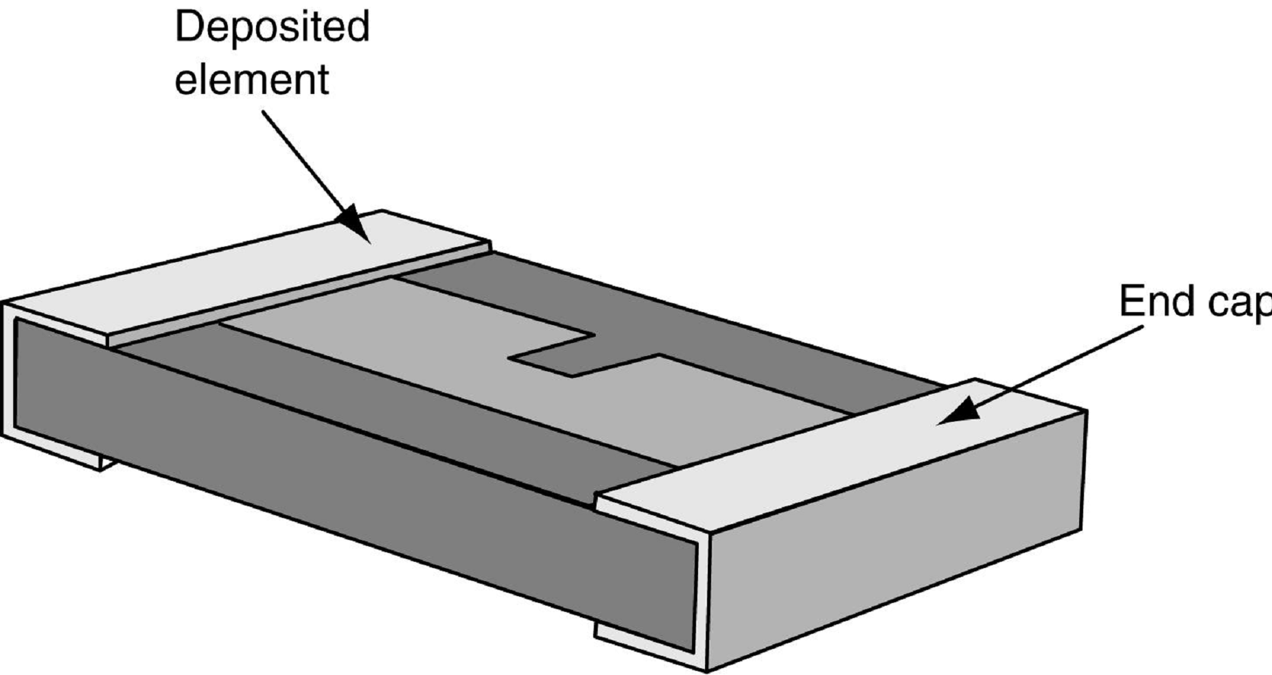 Figure 91: Exposed element
Leaded devices
Surface mounting of leaded (round or rectangular cross section) devices shall be parallel to the board surface.
<<deleted>>
<<deleted>>
Stacking and bonding of heavy devices
Adhesive shall be selected in conformance with clause 7.10.
Some surfaces can be prepared to enhance the adhesion (e.g. by mechanical abrasion).
<<deleted>>
Adhesive shall be mixed and cured in accordance with the manufacturer’s procedures.
The process of applying the adhesive shall be documented by a written procedure or by configured drawings which define the location of the adhesive, the shape and the spread area (between device bottom surface and substrate upper surface).
The adhesive shall not be in contact with the terminal or negate the stress relief of the device, nor come into contact with surrounding devices.
<<deleted and created as recommendation 9.7.9g>>
All devices weighing more than 5 g should be stacked.
- 1 This is to minimize shock and vibration loading on the leads.
- 2 The adhesive compound can be applied either before or after soldering in conformance with the supplier’s process identification document.
Stacking and bonding shall be performed on clean surfaces.
Attachment of conductors to terminals, solder cups and cables
Requirements from clause 9 from ECSSQST7008 shall apply for “Attachment of conductors to terminals, solder cups and cables”.
Soldering to printed circuit boards
General
Requirements from clause 10.1 from ECSSQST7008, clause “Soldering to terminals and printed circuit boards – General” shall apply.
<<deleted>>
<<deleted>>
Solder applications to PCBs
Requirements from clause 10.3 from ECSSQST7008 shall apply for "Solder applications to PCBs".
Wicking
Requirements from clauses 10.3.1, 10.3.2, 10.3.4 and 10.4 from ECSSQST7008 shall apply for "Wicking".
Soldering of SMDs
General requirements
Devices shall not be mounted on flexible substrates as defined “flexible printed boards” in ECSSQST70-10.
Soldering to gold with tin-lead alloys shall not be performed.
- 1 See also requirement 11.5.1h.
- 2 See also clause 8.1.3 "Degolding and pretinning of conductors".
Devices shall not be stacked nor bridge the space between other devices or terminals.
Positioning of devices shall not reduce the specified minimum electrical clearance to adjacent tracks or other metallized elements in conformance with requirements from clause 13 and clause 14 of ECSS-Q-ST-70-12.
Non-axial-leaded devices shall be mounted with all leads seated on a terminal area to ensure mechanical strength.
Solder shall cover and wet the solderable surfaces as specified in clause 13.2.
The footprint shall be designed as the entire terminal of the device lies on its associated footprint on the finished board.
Soldering to gold finish with tin-lead shall not be performed unless the gold finish is thinner than 0,1 μm and all the following conditions are met: - PCB is qualified in compliance with the requirements of clause 6 of ECSS-Q-ST-70-10,
- Assembly verification programme is reviewed and accepted by the Approval Authority, and
- Assembly verification is compliant to requirements of clause 14.
The device footprint on FM shall be same as used in verification programme.
Devices verified by similarity shall use same design principle for the footprint.
The device positioning shall be such that visual inspection can be undertaken.
If visual inspection of a fully populated assembly is not possible, the assembly and inspection shall be made in steps enabling visual inspection.
Artificial stand-off value shall be documented in procedure.
The footprint design shall be done in such way as to avoid, during soldering, contact between the device and the soldering tip.
Any deviation to requirements from clauses 11.5.2 to 11.5.11 shall be demonstrated by verification in compliance with requirements from clause 14.
End-capped and end-metallized devices
There shall be no discernible discontinuities in the solder coverage of the terminal areas of devices.
Solder shall not encase any portion of the body of the device following reflow.
The solder joints to these devices shall meet the dimensional and solder fillet requirements of Table 111 and Figure 111.
End-capped and end-metallized devices having terminations of a square or rectangular configuration (such as chip resistors, chip capacitors and similar leadless discrete devices) can have three or five face terminations, as shown in “a” and “b” in Figure 111.
Table 111: Dimensional and solder fillet for rectangular and square end capped devices
|
Parameter
|
Dimension
|
Dimension limits
|
|
Maximum side overhang
|
A
|
0,1 × W
|
|
End overhang
|
B
|
Not permitted
|
|
Minimum lap contact
|
L
|
75% single terminal length only
|
|
Minimum fillet height
|
E
|
X + 0,3 × H or X + 0,5 mm whichever is less
|
|
Solder Stand-off (elevation)
|
X
|
Present
|
|
Maximum tilt limit
|
C
|
10
|
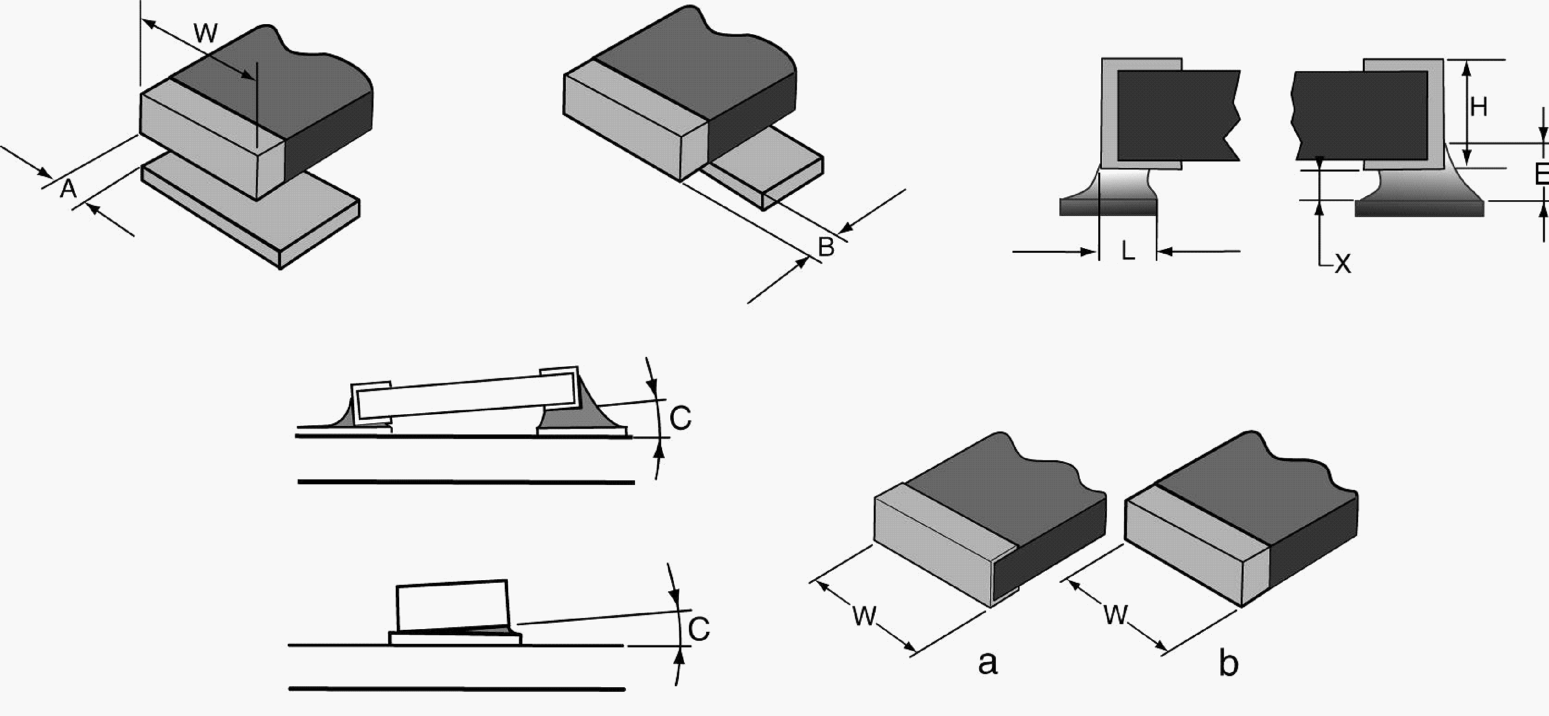 Figure 111: Mounting of rectangular and square end-capped and end-metallized devices
Bottom terminated chip devices
Devices having metallized terminations on the bottom side only shall meet the dimensional and solder fillet requirements of Table 112 and Figure 112.
Solder fillet shall show acceptable wetting on all visible sides.
Table 112: Dimensional and solder fillet for bottom terminated chip devices
|
Parameter
|
Dimension
|
Dimension limits
|
|
Maximum side overhang
|
A
|
0,1 W
|
|
End overhang
|
B
|
Not permitted
|
|
Minimum lap contact
|
L
|
Entire terminal of device
|
|
Solder Stand-off (elevation)
|
X
|
Present
|
|
Maximum tilt limit
|
|
10
|
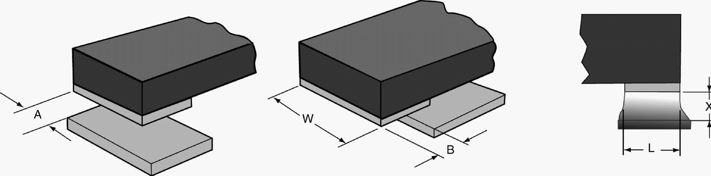 Figure 112: Mounting of bottom terminated chip devices
Cylindrical and square end-capped devices
Solder joints to devices having cylindrical terminations shall meet the dimensional and solder fillet requirements of Table 113 and Figure 113.
Table 113: Dimensional and solder fillet for cylindrical end-capped devices
|
Parameter
|
Dimension
|
Dimension limits
|
|
Maximum side overhang
|
A
|
0,25 D
|
|
End overhang
|
B
|
Not permitted
|
|
Minimum fillet width
|
F
|
0,5 D
|
|
Minimum fillet height
|
E
|
X + 0,3 D or
|
|
Minimum side fillet length
|
L
|
0,5 T
|
|
Stand-off (elevation)
|
X
|
Present up to 0,75 mm
|
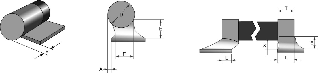 Figure 113: Mounting of cylindrical end-capped devices
Solder joints to devices having square terminations shall meet the dimensional and solder fillet requirements of Table 114 and Figure 114.
Table 114: Dimensional and solder fillet for square end-capped devices
|
Parameter
|
Dimension
|
Dimension limits
|
|
Maximum side overhang
|
A
|
0,25 W (square width)
|
|
End overhang
|
B
|
Not permitted
|
|
Minimum fillet width
|
F
|
0,5 W
|
|
Minimum fillet height
|
E
|
X + 0,3 W or
|
|
Minimum side fillet length
|
L
|
0,5 T
|
|
Stand-off (elevation)
|
X
|
Present up to 0,75 mm
|
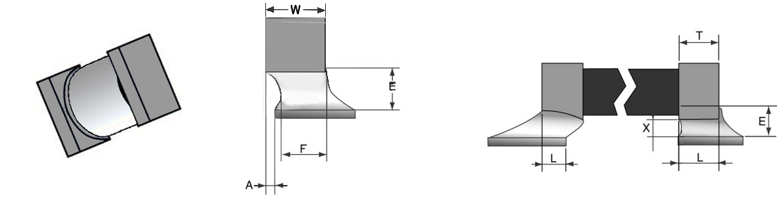 Figure 114: Mounting of square end-capped devices
Castellated chip carrier devices
Joints to castellated device terminations shall meet the dimensional and solder fillet requirements of Table 115 and Figure 115.
- 1 The stand-off enables adequate cleaning beneath the assembled LCCC and also to enhance solder fatigue life (see also clause 9.7.6f)
- 2 <<deleted>>
Table 115: Dimensional and solder fillet for castellated chip carrier devices
|
Parameter
|
Dimension
|
Dimension limits
|
|
Maximum side overhang
|
A
|
Zero
|
|
Maximum fillet length
|
F
|
P (length of the pad)
|
|
Minimum fillet height
|
E
|
0,50 H (H= Castellation metallisation height)
|
|
Solder Stand-off (elevation)
|
X
|
Present
|
|
Underneath lap connection
|
|
Entire terminal of device
|
 Figure 115: Mounting of castellated chip carrier devices
Flat pack and Gull-wing leaded devices with round, rectangular, ribbon leads
Solder joints formed to flat pack and gull-wing leaded devices with round, rectangular, ribbon leads shall meet the dimensional and solder fillet requirements of Table 116 and Figure 116.
Solder fillet shall be visible on the side of the terminal lap connection.
Table 116: Dimensional and solder fillet for gull-wing leaded devices with round, rectangular, ribbon leads
|
Parameter
|
Dimension
|
Dimension limits
|
|
Maximum side overhang
|
A
|
0,1 W
|
|
Minimum distance to footprint edge at toe
|
B
|
0,20 mm
|
|
Minimum distance to footprint edge at heel
|
L
|
0,5 W
|
|
Minimum side joint length
|
D
|
full lap connection soldered
|
|
Minimum heel fillet height
|
E
|
X + T
|
|
Solder Stand-off
|
X
|
Present
|
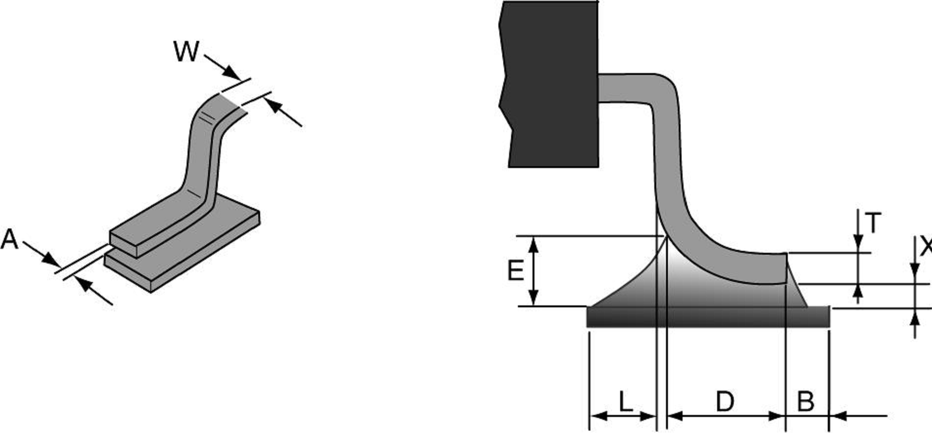 Figure 116: Mounting of gull-wing leaded devices with round, rectangular, ribbon leads
Devices with “J” leads
Solder joints formed to “J” and “V” shaped leads shall meet the dimensional and solder fillet requirements of Table 117 and Figure 117.
Table 117: Dimensional and solder fillet for devices with “J” leads
|
Parameter
|
Dimension
|
Dimension limits
|
|
Maximum side overhang
|
A
|
0,1 W
|
|
Minimum side joint length
|
L
|
1,5 W
|
|
Minimum heel fillet height
|
M
|
X + T
|
|
Maximum stand-off
|
X
|
Present
|
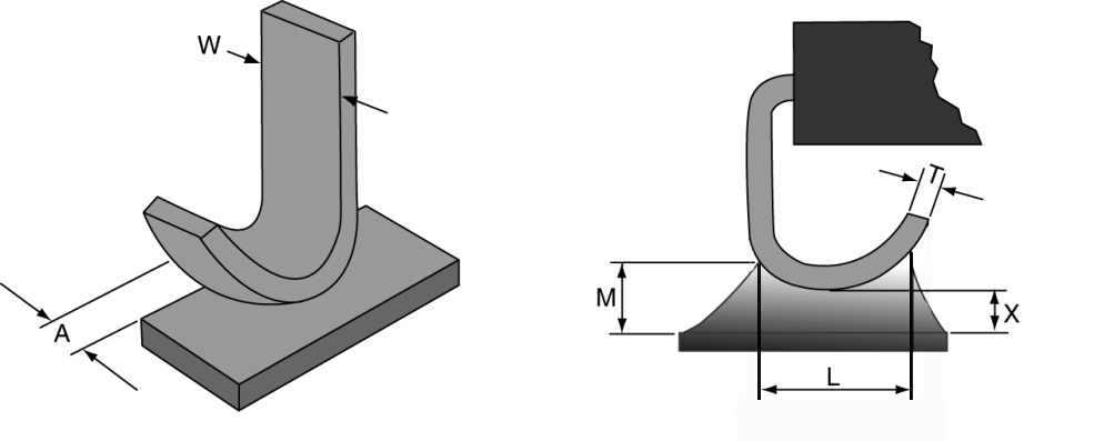 Figure 117: Mounting of devices with “J” leads
Area array devices
The outer row of solder joints to area array devices shall be visually inspected by looking from the side in accordance with the requirements in 11.5.1 and Table 118 and with the rejection criteria specified in clauses 13.3 and 13.4.
Solder joints shall be inspected using X-ray techniques in accordance with clause 6.8.7 and Table 118.
- 1 <<deleted>>
- 2 As it is impossible to visually inspect solder joints to area array devices, reliability of these devices cannot be assured by inspection and rework. Even using X-ray techniques, some types of defect are difficult to detect. Therefore, reliability of these solder joints can only be assured by robust process control.
- 3 Examples of typical area array devices are shown in Figure 118, Figure 119 and Figure 1110.
X-ray techniques shall be used to verify the acceptable wetting, the absence of bridge, solder balls and minimum electrical clearance.
Table 118: Dimensional and solder fillet for area array devices
|
Parameter
|
Dimension limits
|
|
Misalignment
|
No footprint overhang
|
|
BGA ball
|
Collapse of BGA ball does not violate minimum electrical clearance or become less than 0,10 mm.
|
|
Maximum device height
|
Overall height of device does not exceed maximum specified.
|
|
Soldered connection
|
a. BGA balls contact and wet to the land forming a continuous connection
|
|
Solder balls
|
No solder balls.
|
|
Maximum CGA column tilt
|
10 degrees
|
|
D = Ball or column diameter
| |
Figure 118: <<deleted>>
 Figure 119: Typical ceramic area array showing ball grid array configuration on left and column grid array on right (CBGA & CCGA)
 Figure 1110: Typical assembled CCGA device
Devices with ribbon terminals without stress relief
Solder joints formed shall meet the dimensional and solder fillet requirements of Table 119 and Figure 1111.
The degolding and pretinning zone shall be outside the PCB footprint.
This is to ensure that the degolding and pretinning has been performed such that the solder fillet is not in contact with the gold or AuSn intermetallic.
Table 119: Dimensional and solder fillet for devices without stress relief
|
Parameter
|
Dimension
|
Dimensions Limits
|
|
Maximum side overhang
|
A
|
≤ 0,1 x W
|
|
Minimum distance to footprint edge at toe
|
B
|
≥ 0,20 mm
|
|
Stand-off
|
X
|
Present
|
|
Minimum side joint fillet
|
D
|
3xW with full lap soldered connection
|
|
Maximum tilt
|
C
|
10°
|
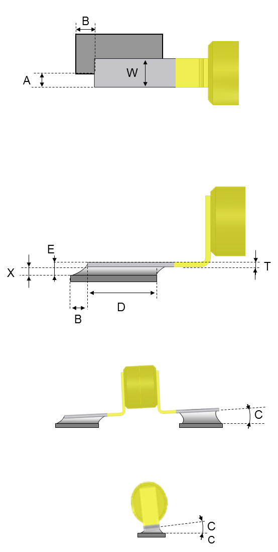 Figure 1111: Mounting of devices without stress relief
L-Shape inwards devices
Devices having L-shape inwards terminals shall meet the dimensional and solder fillet requirements of Table 1110 and Figure 1112.
Solder fillet shall be visible on the side of the terminal on the connection.
The device shall be centred on its footprints such as the minimum lap contact length is fulfilled.
Table 1110: Dimensional and solder fillet for “L-shape inwards” devices
|
Parameter
|
Dimension
|
Dimension limits
|
|
Minimum fillet height, heel
|
E
|
(0,25 x H)+X or X +1mm whichever is less
|
|
Minimum distance to footprint edge
|
K
|
0,2 mm
|
|
Minimum Lap contact length
|
L
|
75% terminal of device, limited to one side
|
|
Stand-off (elevation)
|
X
|
Present
|
|
Side of terminal wetting
|
|
Evidence of solder wetting
|
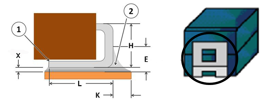 Figure 1112: Mounting of devices with “L-shape inwards” leads (1 = Toe, 2 = Heel)
Stacked modules devices with leads protruding vertically from bottom
Stacked modules devices shall meet the dimensional and solder fillet requirements of Table 1111 and Figure 1113.
Solder fillet shall be visible in the heel fillet.
Table 1111: Dimensional and solder fillet for stacked modules devices with leads protruding vertically from bottom
|
Parameter
|
Dimension
|
Dimension limits
|
|
Maximum side overhang
|
A
|
0,1 W
|
|
Minimum distance to footprint edge at toe
|
B
|
0,20 mm
|
|
Minimum distance to footprint edge at heel
|
L
|
0,5 W
|
|
Minimum side joint length
|
D
|
full lap connection soldered
|
|
Minimum heel fillet height
|
E
|
Wetting solder visible in the heel fillet, X+ 0,5T
|
|
Solder Stand-off
|
X
|
Present
|
|
Lead thickness
|
T
|
|
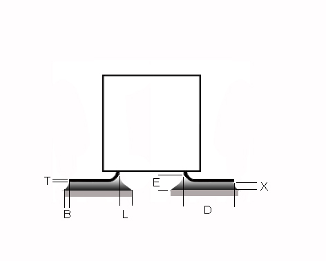 Figure 1113: Mounting of stacked modules devices with leads protruding vertically from bottom
Leaded device with plane termination
Leaded devices with plane termination shall meet the dimensional and solder fillet requirements of Table 1112 and Figure 1114.
Solder fillet shall be visible in the heel fillet.
Termination plane shall be inspected with X-ray equipment according to clause 6.8.7.
Plane termination shall meet X-ray criterion according to requirements 13.4a.2 to 13.4a.5.
Table 1112: Dimensional and solder fillet for leaded devices with plane termination
|
Parameter
|
Dimension
|
Dimension limits
|
|
Maximum side overhang
|
A
|
0,1 W
|
|
Minimum distance to footprint edge at toe
|
B
|
0,20 mm
|
|
Minimum distance to footprint edge at heel
|
L
|
0,5 W
|
|
Minimum side joint length
|
D
|
full lap connection soldered
|
|
Minimum heel fillet height
|
E
|
X + T
|
|
Solder Stand-off
|
X
|
Present
|
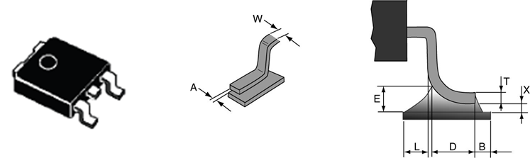 Figure 1114: Mounting of leaded devices with leads with plane termination
Moulded magnetics
Moulded magnetics devices shall meet the dimensional and solder fillet requirements of Table 1111 and Figure 116.
Solder fillet shall be visible in the heel fillet.
<<deleted>>
<<deleted>>
<<deleted>>
Figure 1115: <<deleted>>
<<deleted>>
<<deleted>>
<<deleted>>
<<deleted>>
Cleaning of PCB assemblies
General
Requirements from clause 11.1 from ECSSQST7008, clause “Cleaning of PCB assemblies – General” shall apply.
Ultrasonic cleaning
Requirements from clause 11.2 from ECSSQST7008 shall apply for "Ultrasonic cleaning".
Monitoring for cleanliness
Requirements from clause 11.3 from ECSSQST7008 shall apply for "Monitoring for cleanliness".
Final inspection
General
Each soldered connection shall be visually inspected in accordance with the criteria specified in the requirements 13.1d, 13.1e, and 13.1f
<<deleted>>
<<deleted>>
Devices and conductors shall not be physically moved to aid inspection.
The substrate, solder joint, devices and device position, shall be inspected in accordance with the requirements in clause 11.5.
Annex I includes examples of acceptable and unacceptable workmanship.
The assembly shall be visually inspected in two steps with the following methodology:
- Visual inspection of the assembly is aided by magnification appropriate to the size of the connections between 4x and 10x.
- Detailed inspection is performed with a minimum magnification 20x.
Additional magnification shall be used to resolve suspected anomalies or defects up to 40x.
X-ray inspection shall be applied when there are hidden solder joints that are not visually accessible.
Acceptance criteria
Acceptable solder connections shall be characterised by:
- clean, smooth, satin to bright undisturbed surface,
- solder fillets between conductor and termination areas as described in clause 11.5,
- visible contour of wires and leads such that their presence, direction of bend and termination end can be determined,
- complete wetting as evidenced by a low contact angle between the solder and the joined surfaces,
- acceptable amount and distribution of solder in accordance with clause 11.5,
- absence of any of the defects mentioned in clauses 13.3 and 13.4.
Annex I includes examples of acceptable and unacceptable workmanship.
Visual rejection criteria
The following are some characteristics of unsatisfactory conditions, any of which shall be cause for rejection:
- charred, burned or melted insulation of devices,
- conductor pattern separation from circuit board,
- burns on base materials,
- <<deleted>>
- excessive solder (including peaks, icicles and bridging), see clause 11.5,
- flux residue, solder splatter, solder balls, or other foreign matter on circuitry, beneath devices or on adjacent areas,
- dewetting,
- insufficient solder, see clause 11.5,
- pits, holes or voids where bottom is not visible,
- granular or disturbed solder joints,
- fractured or cracked solder connection,
- cut, nicked, gouged or scraped conductors or conductor pattern,
- <<deleted>>
- <<deleted>>
- damaged conductor pattern,
- bare copper or base metal, excluding the ends of cut wire or leads or sides of tracks and soldering footprints on substrate,
- soldered joints made directly to gold-plated terminals or gold-plated conductors using tin-lead solders,
- cold solder joints,
- device body embedded within solder fillet,
- open solder joints (e.g. tombstoning),
- probe marks present on the metallization of chip devices caused by electrical testing after assembly,
- glass seal does not conform to MIL-STD-883 Method 2009,
- any nonconformance with clause 11.5,
- measling which violates the minimum insulation distance,
- delamination, except within region of the breakout regions for multi-panel processed,
- exposed base metal excluding area of cut leads in the soldered connection,
- cracks detected in glass diodes outside the relevant devices procurement standard,
- bent connector pins outside the relevant devices procurement specification,
- damage of the lead, device or PCB beyond that defined in the procurement standard of the item,
- degraded insulation material of the connector in contact area,
- bubble or void in the conformal coating or potting that are bridging conductive elements,
- bubble, void or delamination in conformal coating and or potting between high voltage conductors,
- lack of intended conformal coating,
- unintended and continuous adhesive forming a bridge in contact with terminals, component body or solder joints,
- excessive degolding,
- insufficient degolding,
- direct bonding on glass device body with epoxy,
- separation of adhesive from the bonded surface,
- separation of conformal coating from the surface,
- any longitudinal misalignment on sensitive devices,
- longitudinal misalignment of end capped and end metallized devices,
- presence of cracks in the ceramic of devices or cover of device.
- 1 For requirement 13.3a.29, end cap metallization peeling crack in device, missing metallization are examples of damage.
- 2 For requirement 13.3a.29, cracks in ceramics mainly occur in chip capacitors, and leadless device with thermal plane termination.
- 3 For the requirement 13.3a.32, high voltage applications are defined in ECSS-E-HB-20-05.
X-ray rejection criterion
The following are some characteristics of not acceptable conditions from X-ray inspection, utilizing equipment defined in clause 6.8.7, any of which shall be cause for rejection:
- criteria and dimensions outside the limits given in Table 118 for area array devices,
- bridges and other unintended metallic materials,
- non-wetting of the solder,
- cumulative voids greater than 25 % by area of the solder joint,
- a single void which traverses either length or width of the terminal and exceed 10 % of the total area.
For the requirement 13.4a.2 solder balls are a typical example of unintended metallic material.
Any deviation to requirement 13.4a.4 shall be demonstrated by verification in compliance with requirements from clause 14.
Warp and twist of populated boards
<<deleted>>
The PCB assembly shall be supported during handling and transportation in order to avoid any mechanical stress on the assembly or component damage.
Mechanical support can be provided by spacer and frame.
The PCB shall not be forced during integration to compensate warp and twist.
Shims or spacers can be used to accommodate warp and twist during integration.
Inspection records
The result of the final inspection shall be recorded on the shop traveller.
Verification procedure
General
The supplier shall establish a verification programme in accordance with the DRD from Annex G for approval by the Approval Authority.
Requirement G.2.1b gives possibility to tailor verification programme.
The supplier shall demonstrate verification for each combination of substrate material, PCB footprint, SMD type, soldering technique applied, stacking and bonding, lead forming configuration, , solder mask and conformal coating as used on FM.
Substrate materials are defined in Table 6-1 of ECSS-Q-ST-70-12.
<<deleted>>
<<deleted>>
<<deleted>>
The verification shall be performed on at least three devices except for the sensitive devices where five parts are used per configuration in the verification programme.
- 1 For the devices listed in the ESCIES sensitive list that have not been demonstrated to be none sensitive by the supplier the first verification test plan is with five devices.
- 2 Machine reflow, hand soldering are examples of different assembly methods.
The supplier’s repair process including removing and replacing of one of each type of mounted device shall be submitted to verification testing. - 1 Verification of the number of repairs as permitted in ECSS-Q-ST-70-28.
- 2 The supplier has the option to perform more than one repair for each type of device.
<<deleted>>
<<deleted>>
<<deleted>>
Verification testing of commercial devices shall be performed for each lot in conformance with this clause.
A repair, not included in ECSSQST70-28, shall be submitted to a verification programme.
Verification of the assembly shall be performed with a nominal method and a repair method for each device.
Standard manual method can cover a range of processes in addition to hand soldering e.g. hot gas station, IR station.
Collective assembled devices shall not be reworked neither repaired.
The PCB verification test vehicle shall be representative of the FM footprint configuration and connections of the hardware.
Terminations to be microsectioned shall be connected to the internal PCB layers.
The terminations to be microsectioned are described in Table 142.
The verification of area array devices shall meet the requirements of clause 14.9.
For each type of device, the repair shall be performed on the largest device.
The repair shall be performed only on the devices being assembled by standard manual method.
No repair verification is needed on the devices being assembled by machine method as this is covered under the standard manual soldering verification method.
The supplier shall maintain a list of sensitive devices.
Sensitive devices shall be submitted to re-verification every four years to monitor the stability of the assembly.
The re-verification of sensitive devices specified in the requirement 14.1u may be performed on limited verification programme performed on worst case configuration identified during initial verification.
- 1 One substrate, one package per device type, three samples per device.
- 2 For leadless devices, mechanical testing can be omitted.
- 3 Non-destructive characterization can be proposed as alternative to microsection.
The verification sample shall be submitted to two nominal soldering method reflows when reflow is performed on the both PCB sides of the FM.
The supplier has the option to flip the board for the second reflow to demonstrate the flight configuration.
The device type classification shall be in accordance with Table 141.
Table 141: Device type classification
|
Device type
|
Classification
|
|
Rectangular and square end-capped or end-metallized device with rectangular body
|
Leadless chip
|
|
Cylindrical and square end-capped devices with cylindrical body
|
Leadless chip
|
|
Bottom terminated chip device
|
Leadless
|
|
Castellated chip carrier device
|
Leadless
|
|
Flat pack and Gull-wing leaded device with round, rectangular, ribbon leads
|
Leaded
|
|
Moulded magnetics
|
Leaded
|
|
“J” leaded device
|
Leaded
|
|
Area array devices
|
AAD
|
|
Devices with ribbon terminals without stress relief (flat lug leads)
|
Leaded
|
|
Device with Inward formed L-shaped leads
|
Leaded
|
|
Stacked modules devices with leads protruding vertically from bottom
|
Leaded
|
|
Leaded device with plane termination
|
Leaded
|
Verification by similarity
<<deleted>>
<<deleted>>
<<deleted>>
<<deleted>>
<<deleted>>
<<deleted>>
<<deleted>>
<<deleted>>
<<deleted>>
<<deleted>>
<<deleted>>
General
A package shall be identified as the same family in case the following conditions are met:
- the lead pitch, nominal thickness, nominal width and materials composition are identical,
- the coated lead finishes on the termination are identical,
- the bending dimensions and shape are identical,
- the packages are constructed from the same materials.
- 1 Glass to metal sealed, glass sealed side-brazed, top-brazed, and bottom-brazed packages are different families.
- 2 Dual side pin arrangements are different to quad side pin families.
For flat pack, verification by similarity may apply even if the lead materials are different.
Conditions for similarity
Verification by similarity shall not apply to commercial devices.
Verification by similarity shall not apply to castellated devices.
Some resistors networks and LCCs are castellated devices examples
Verification by similarity for leadless chip devices shall not be declared successful until the following conditions are met:
- device size is between the length Lmax and the width Wmax of verified component,
- the device is thinner than the maximum height verified,
- the ceramic material type is identical,
- the metallization of the termination and the barrier layers on devices is identical,
- the device manufacturer is identical.
- 1 for item 1: for example, 0402 – 2220 does not qualify 1825 as the width is outside the max 20 verified.
- 2 for item 2: ceramic chip capacitors can be very sensitive to mounting conditions. Generally, type 1 chip capacitors show less sensitivity to mounting constraints than Barium Titanate based type 2 chip capacitors. This sensitivity is design and process related and can therefore vary from one manufacturer to another. Within a manufacture type 2 range, one or more ceramic material can be used but one can say that generally the highest end of the capacitance ranges is the most sensitive to mounting conditions. In order to increase capacitance value for a given chip format with a specified maximum chip thickness, manufacturers increase the number of dielectric layers, thus increasing the volume ratio between electrode material and ceramic, which is not favourable in terms of sensitivity to mounting constraints.
- 3 for item 2: it is therefore impossible to apply similarity rules between type 1 and type 2 ceramic chip capacitors as well as between different manufacturers. It is also good practice to select in priority the highest capacitance values in a class or type 1 or type 2 ceramic capacitors range to be submitted to assembly verification.
- 4 for item 3: type refers only to type 1 or type 2 capacitor.
Verification by similarity for leaded devices, cylindrical or square end-capped devices with cylindrical body and device with inward formed L-shaped leads shall be valid in case the following conditions are met: - the devices are from the same family in conformance with the requirements from the clause 14.2.1,
- devices are smaller than the verified Lmax and Wmax,
- demonstration that small package is not damaged during the placement on PCB.
The dimension L is the distance between the outermost leads of the device and W is the device width.
Verification by similarity for leadless device with thermal plane termination shall be valid in case the following conditions are met:
- smaller than the verified Lmax and Wmax,
- the construction of the device is identical to that verified,
- the materials are identical.
The outline dimensions of the device are length, L and width W.
Verification by similarity for area array devices shall be valid in case the following conditions are met:
- lower number of columns,
- the same pitch,
- same column dimensions,
- same columns distribution,
- same column materials,
- same column construction,
- same column manufacturer,
- same column assembly process,
- lower mass,
- same material and same package construction,
- same shape.
Verification programme
The verification programme as shown in Figure 141 shall consist of:
- Visual inspection in conformance with clause 13.
- Vibration and shock testing in conformance with clause 14.5.
- Temperature cycling in conformance with clause 14.6 except for area array devices .
- Microsectioning in conformance with clause 14.7.
- For area array devices, temperature cycling in conformance with requirements from clause 14.9.
- Cleanliness in conformance with requirement 14.14b.
- 1 Note to item 2: Mechanical testing according to this standard gives an indication of the reliability of the product in actual applications. It is unlikely that the test vehicle represents every flight configuration (size of the board, damping of the board, stiffening of board, number of board layers). The deflections, amplitudes, transmissibilities, radii of curvature experienced by SMDs under shock and vibration are totally dependent on the board to which they are mounted. Because each space project has its own unique shock and vibration requirements it is impossible to determine appropriate test levels without testing actual electronic boxes.
- 2 Note to item 3: Temperature cycling is performed to ensure that the SMDs, substrates, solder alloys and associated stacking compounds and conformal coatings are suitable for the operational lifetime of the spacecraft.
The supplier shall present a verification programme for approval.
Owing to the different modes of failure resulting from vibration and temperature cycling, the supplier can use any sequence of environmental testing.
Removal and replacement shall be verified on the repair assembly method.
When mechanical bonding is underneath the device, microsectioning of one device may be performed after vibration and 50 thermal cycles to justify the integrity of the bonding.
The device can be one of the three assembled devices.
The devices used for the verification shall be in compliance with list of devices from the Table H-1.
It is under the responsibility of the company to ensure that the soldering method and temperature is compliant with the manufacturer datasheet and or technical notes.
The devices soldered by collective process shall not be reworked.
Reworking of collective assembled solder joint shall be decided during the MIP1 in compliance with Figure 141.
The environmental conditions of the mission including ground testing shall be reviewed to ensure the verification programme envelops the mission conditions.
Supplier shall ensure that the conditions associated with long term storage, extensive ground testing, mechanical stress after launch, high temperature application with or without thermal cycles are assessed.
The supplier shall organise a Verification review (VR) with the Approval Authority during which Verification programme is reviewed and approved.
The PCB design is reviewed to ensure compliance with requirements from clause 14.1.
Prior to start of verification assembly the supplier shall organise a Manufacturing readiness review (MRR) with the Approval Authority.
During the review, the Approval Authority can check that the verification programme is approved by all parties and that all open actions are closed.
The supplier shall organise a Mandatory inspection point (MIP1) with the Approval Authority prior to any conformal coating with five days notification.
The Approval Authority can delegate the MIP1 to the supplier.
Prior to any environmental testing the supplier shall organise with the Approval Authority an action review during which the MIP and outstanding actions are reviewed, with five days notification.
The Approval Authority can delegate the action review to the supplier.
The supplier shall organise with Approval Authority a Mandatory Inspection Point (MIP2) at the completion of the environmental test with five days notification.
The Approval Authority can delegate the MIP2 to the supplier.
The supplier shall organize with the Approval Authority a Test review board (TRB) during which the environmental tests results are reviewed.
The Approval Authority may delegate the TRB to the supplier.
The supplier shall organise with the Approval Authority a final verification review in conformance with requirements from clause 14.15.5.
The Assembly processes can be reviewed during the meeting in order to have the PID issued. Verification of closure of the actions identified during the audit of the manufacturing line.
Any nonconformance or major change with reference to the verification plan shall be notified to the Approval Authority within one week.
NRBs shall be organised by the supplier.
The schedule of the verification activities shall be provided and maintained.
 Figure 141: Verification programme flow chart (standard flow)
Electrical testing of devices
<<deleted>>
General
Except the cases specified in the requirements 14.4.1b and 14.4.1c, the supplier may propose electrical monitoring as an alternative method, for each assembly configuration, including the repair assembly method, to achieve verification providing the following conditions are met:
- one device for initial microsectioning except the case for sensitive and leadless devices,
- for sensitive devices, a minimum of five devices to be assembled,
- minimum number of 32 devices for electrical monitoring,
- all solder terminations are continuously electrically monitored throughout the temperature cycling,
- minimum of 1500 thermal cycles in accordance with requirements from the clause 14.6,
- the number of completed cycles for each failed device is recorded.
Electrical monitoring shall be performed for ceramic hermetic area array devices in conformance with requirements in clause 14.9.
Capacitors and “SMD – xx” devices shall be excluded from electrical monitoring.
Capacitor and “SMD–xx” devices such SMD05, SMD1, SMD2 and SMD5C are excluded as the failure mechanism is crack in ceramic.
First failure in case number of cycles < 1500 shall be identified as the device assembly verification limitation.
Any failed device shall be subjected to failure analysis.
The electrical value of devices shall be selected to ensure detection of anomaly in the solder joint.
- for resistors zero ohm or the lowest value in the procurement specification,
- for other types, custom daisy chain. During thermal cycling, a drift of less than 10 % of resistance shall be accepted when the electrical monitoring is performed and referenced to the first five cycles recorded values.
Depending on application the acceptable drift of resistance can be adapted.
For each assembly method and type of devices at least 32 devices shall be assembled for electrical monitoring.
- 1 Machine reflow, hand soldering are the examples of assembly method.
- 2 The assembly of the capability and the electrical verification samples can be made on the same board.
If capability and electrical monitoring samples are on the same board they shall be separated before the microsectioning of the capability samples and before the environmental tests for the electrical verification samples.
Illustration is given in the flow diagram of Figure 142.
Capability samples may be excluded from the programme if it can be demonstrated through previous verification heritage.
Microsectioning shall be performed in accordance with requirements from clause 14.7.
Vibration and shock testing shall be performed in conformance with requirements from clause 14.5.
 Figure 142: Verification programme flow chart (electrical testing)
Vibration and shock
Requirements from clause 13.2 from ECSSQST7008 shall apply for "Vibration".
For area array devices, the shock levels shall be set to meet the intended mission with margin, except the case specified in the requirement 14.5c.
For area array devices shock may be omitted when the mechanical design can demonstrate robust margin.
The use of dedicated mechanical stiffener is an example of such design.
For shock, sensitive devices shock testing shall be added to the verification programme flow.
Examples of shock sensitive devices can be found in ECSS-E-HB-32-25.
When shock testing is required as defined in 14.5d then the shock levels shall be set to meet the intended mission with margin.
The levels and duration of the vibration shall be provided.
It is the responsibility of the contractor to ensure that the levels applied are sufficient to cover the mission.
The levels and duration of the shock shall be provided by supplier.
The mounting configuration of the PCB for the vibration tests shall be identified.
The PCB shall be mounted such that the deflection and acceleration is representative of the FM.
The accelerometers shall be placed on the PCB as well as on the base plate in order to determine the acceleration of the PCB.
Temperature cycling test
Requirements from clause 13.3 of ECSSQST7008 “Temperature cycling test” shall apply for the thermal profile.
The total number of temperature cycles shall be 500, except for area array devices and devices verified by electrical monitoring when clause 14.9 and 14.4 is applicable.
The monitoring temperature sensor shall be attached to the surface of the printed circuit board.
<<deleted>>
Compliance from -55 °C to +85 °C for mission shall be stated.
Microsection
<<deleted, modified and moved to 14.7.2>>
<<deleted, modified and moved to 14.7.2>>
<<deleted>>
<<deleted, modified and moved to 14.7.2>>
<<deleted, modified and moved to 14.7.2>>
Microsection facilities
Approval Authority should make available the list of laboratories to perform microsection.
The list of available laboratories is on ESCIES website.
Microsections shall be performed by a laboratory specified in 14.7.1a except the case specified in the requirement 14.7.1c.
When in-house or other non-listed microsection facilities are used, the company shall demonstrate the following:
- the laboratory capability on a representative sample without conformal coating is provided,
- a report with associated microsections is sent to the Approval Authority for review and assessment of quality of microsectioning,
- representative samples include chip devices, LCCs and FPs.
Microsectioning
Microsections shall be performed in compliance with the Table 142.
The microsection shall be inspected with a magnification of 50 to 200 times except the case specified in the requirement 14.7.2m.
At least one microsection shall be made per assembly configuration after environmental testing on each type of device, size and assembly processes and soldering processes.
Successive polishing planes can be performed.
Additional microsections may be requested in case of cracks or other features detected during the first microsection sample or by request from the Approval Authority.
The microsection shall be done on the device having the worst solder joint appearance as identified at MIP2.
In case the microsection shows a crack more than 75% of acceptable crack, a second device shall be microsectioned.
In case the second microsection shows a crack more than 75% of acceptable crack a third device shall be microsectioned.
In case the third microsection shows a more than 75% of acceptable crack device shall be classified as sensitive.
For sensitive devices five devices shall be microsectioned per assembly configuration.
Number of microsections as specified in requirement 14.7.2i may be reduced based on Approval Authority agreement.
The integrity of the assembly shall be assessed by microsectioning.
Integrity covers PCB, solder joints, adhesives, packages.
Adhesive for thermal or mechanical purpose underneath a device shall be microsectioned.
The microsection for devices with small stand-off should be inspected with magnification up to 500 times.
Examples of small stand-off devices are LCCs, chip resistors.
The Approval Authority shall have access to the moulded microsection and pictures.
The microsections and other devices shall be stored for a period of at least 10 years.
Stored samples can assist the analysis of in-service failures.
Table 142: Device microsection location
|
SMD type
|
Example device
|
Cross section planes
|
Example of views at min and max magnification
|
|

|
Terminal to cross section
|
|
|
|
Rectangular and square end-capped or end-metallized device with rectangular body
|
chip resistors
|
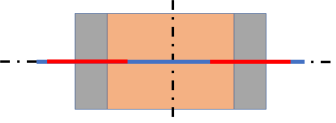
|
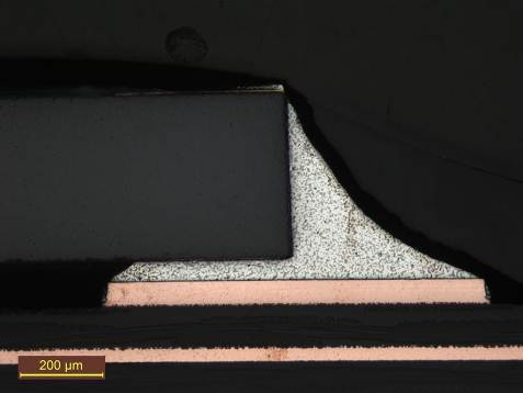
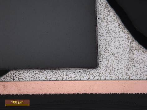
x50 x200 |
|
chip capacitors
|
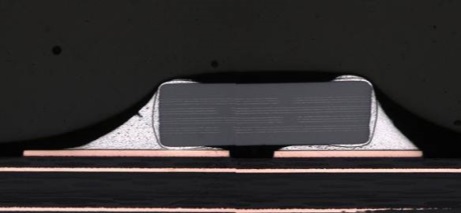
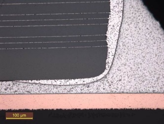
x50 x200 | ||
|
Cylindrical and square end-capped devices with cylindrical body
|
MELF
|

|
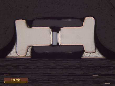
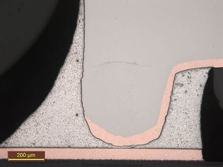
x50 x100
|
|
Bottom terminated chip device
|
SMD0.5, SMD1, SMD2, SMD0.2, SMD0.22
|
 +
|
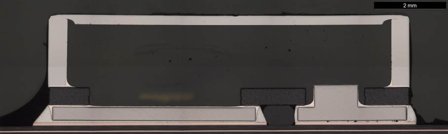
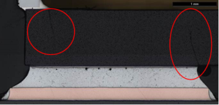
x25 x50
|
|
Bottom terminated chip device
|
Quad Flat Pack No lead (QFN)
|
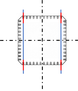
When thermal plane is present, the third microsection is in the middle axis:
|
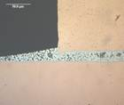
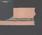
|
|
Castellated chip carrier device
|
LCC3
|
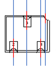 With ground connection (microsection to be done in the middle of castellation)
|
x100 x200
|
|
LCC6
|
|
||
|
LCC with termination on 4 faces
|
|
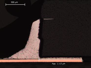
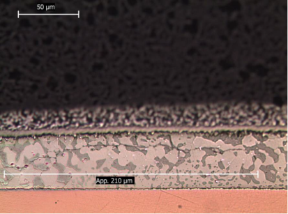
x100 x500 | |
|
Resistor array
|
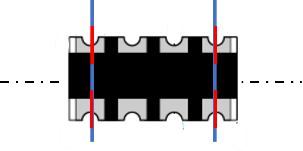
|
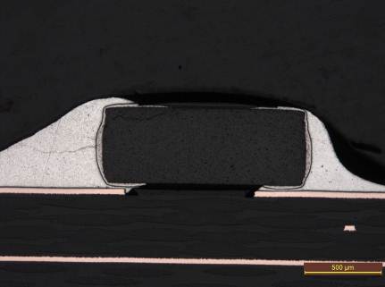
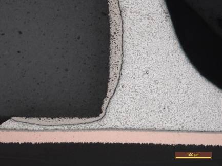
x20 x100 | |
|
Flat pack and Gull-wing leaded device with round, rectangular , ribbon leads
|
SOT23
|
|
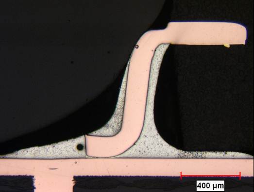
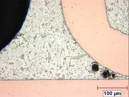
x50 x200 |
|
CQFP + MQFP
|
Centre micro-section to be done only when device is bonded. |
x50 x100
| |
|
|
FP, SO, SOIC
|
Centre micro-section to be done only when device is bonded. |
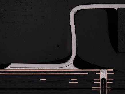
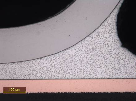
x50 x200
|
|
FP with spider leads
|
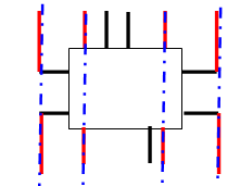
|
||
|
Moulded magnetics
|
1553 interface transformers or specific transformers
|
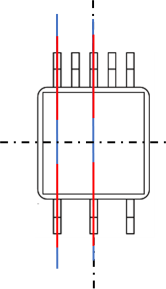
Microsection plane in one edge. Additional microsection depending on lead configuration (different dimensions or shape) |
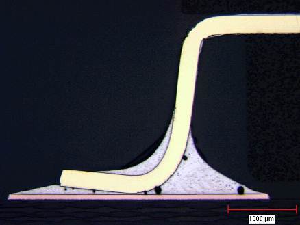
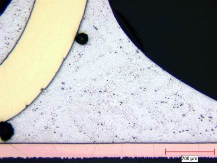
x25 x100
|
|
“J” leaded device
|
ceramic leaded chip carriers (CLCC) and plastic leaded chip carriers (PLCC)
|
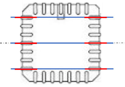
|
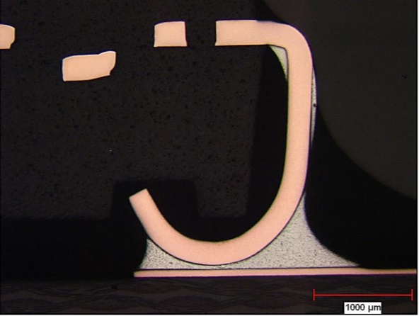
|
|
Area Array devices (Capability Phase only)
|
CCGA
|
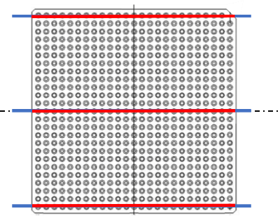
|
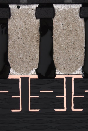
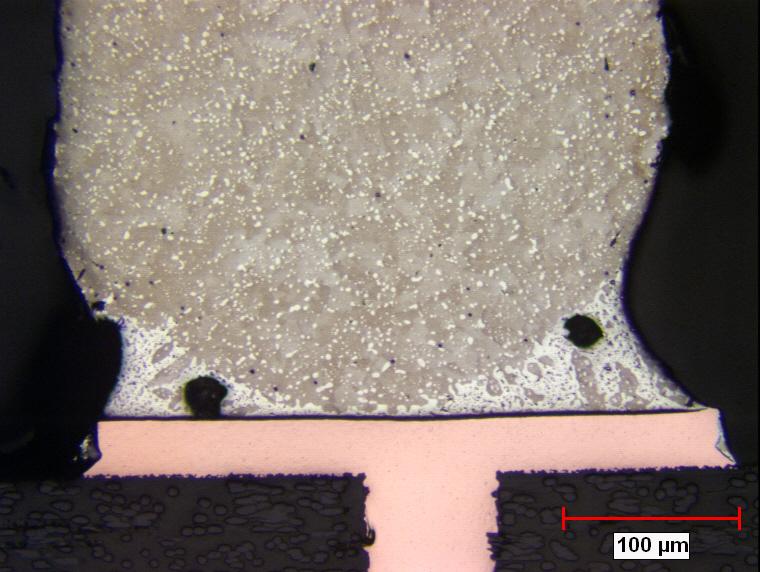
x25 x100
|
|
Devices with ribbon terminals without stress relief (flat lug leads)
|
|
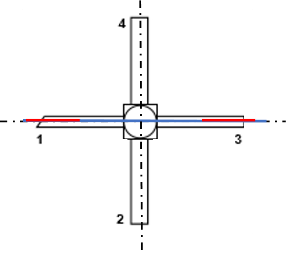
|
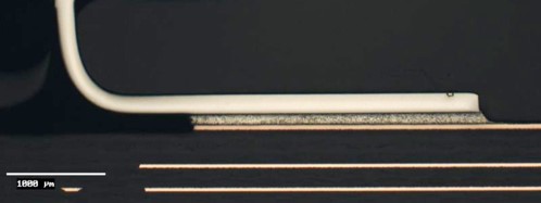
|
|
Device with Inward formed L-shaped leads
|
Tantalum chip capacitor
|
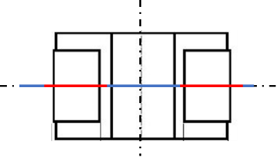
|

|
|
Stacked modules devices with leads protruding vertically from bottom
|
|
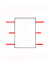
Can be reduced when package is less than 50 leads |
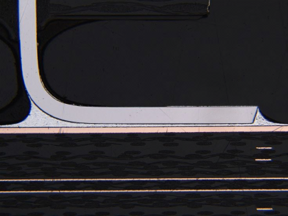
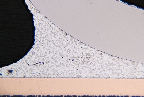
x25 x200 |
|
Leaded device with plane termination
|
DPAK/TO252
|
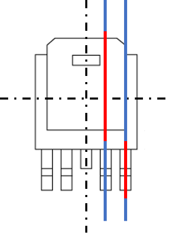 X Ray+ micro section (lead + plane)
|
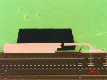
x20
|
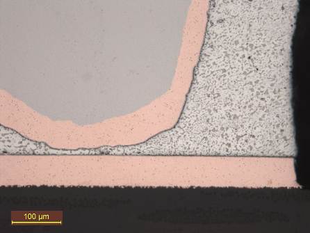
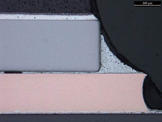
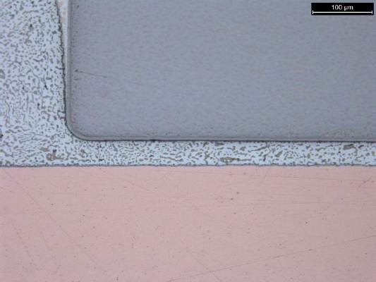
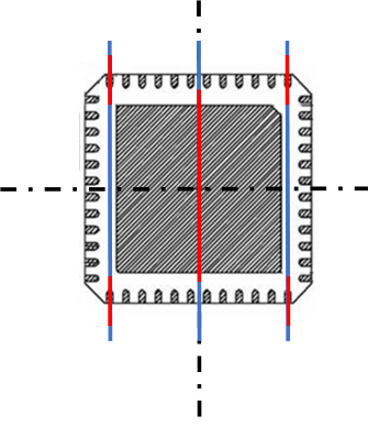

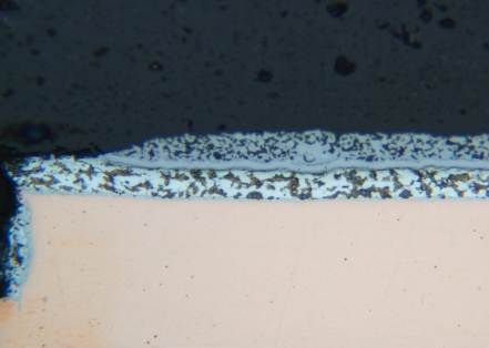
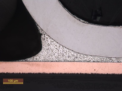

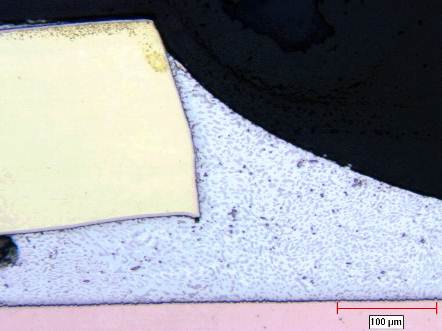
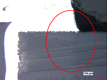
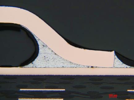
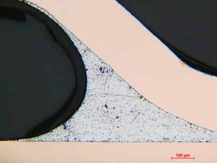
<<deleted>>
<<deleted>>
<<deleted>>
Special verification testing for hermetic ceramic area array packages
<<deleted>>
<<deleted>>
<<deleted>>
<<deleted>>
<<deleted>>
<<deleted>>
<<deleted>>
<<deleted>>
General
The assembly verification of hermetic ceramic AADs shall be divided in the following two parts, as shown in Figure 143.
- electrical monitoring, and
- demonstration of capability.
- 1 The purpose of the capability samples is to show that the PCB integrity and the device are intact after the assembly and repair of AAD and environmental testing (vibration, mechanical shock and 500 temperature cycles). A crack in the columns or balls is not considered as reason for rejection.
- 2 Once the capability samples show a satisfactory result the verification of AAD can commence.
- 3 Capability samples can be excluded from the programme if the supplier can demonstrate through previous verification heritage.
When nominal and repair processes are identical then total number of parts during verification may be reduced to five with three assembled and two repairs among the three assembled.
The verification shall be performed with daisy chain devices to demonstrate a reliable electrical function of the PCB and the package interface throughout the environmental test campaign.
Environmental test campaign to include vibration, mechanical shock and 1500 temperature cycles.
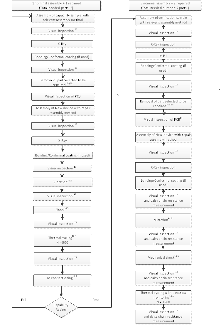 Figure 143: Verification programme flow chart (AAD)
Evaluation of capability samples
The supplier shall manufacture and demonstrate that the two capability samples are in conformance with the requirement 14.9.4i before the manufacture of the verification samples using daisy chain devices can be initiated.
The PCB material, PCB build-up, foot print and devices used as capability samples shall be representative for the FM of the hardware.
One device shall be assembled in the relevant reflow process.
The supplier can use daisy chain packages for the capability assessment with or without electrical monitoring.
The device shall be removed and replaced with a new device using the repair process.
The device shall be inspected in conformance with requirements from the clause 11.5.8.
The device shall be submitted to vibration testing in conformance with requirements from the clause 13.2 of ECSS-Q-ST-70-08.
The device shall be submitted to three mechanical shock axes in conformance with requirements 14.5b and 14.5c.
The device shall be submitted to 500 thermal cycles in conformance with requirements from the clause 13.3 of ECSS-Q-ST-70-08.
After environmental tests completion, microsectioning of the device shall be performed to demonstrate PCB integrity in the AAD area with respect to:
- ECSS-Q-ST-70-10,
- Damage to the device outside the procurement specification,
- Footprint lifts,
- Cracks in laminate,
- Cracks in via,
- Cracks in track,
- Delamination’s in the PCB,
- Measling in the PCB,
- Cracks in bonding if used.
Verification
The PCB material, PCB build-up, foot print and daisy chain devices used for the verification shall be representative for the FM of the hardware.
For each assembly method and mounting configuration five devices shall be assembled.
Two of the assembled devices shall be removed and replaced with a new device using the repair process.
The devices shall be inspected in conformance with requirements from the clause 11.5.8.
The five devices shall be submitted to vibration testing in conformance with requirements from the clause 13.2 of ECSS-Q-ST-70-08.
The five devices shall be submitted to three mechanical shock pulses in each direction in conformance with requirements 14.5b and 14.5c.
The five devices shall be submitted to 1500 thermal cycles with temperature conditions in conformance with requirements from the clause 13.2 of ECSS-Q-ST-70-08.
Resistance measurement should be done, at ambient, before and after any mechanical testing.
Electrical monitoring of the daisy chain shall be performed during the 1500 thermal cycling.
The electrical monitoring shall be continuous throughout all 1500 cycles.
The sampling time of the electrical measurement shall be maximum 10 s throughout the 1500 cycles.
Different electrical monitoring methods can be agreed with Approval Authority.
The maximum increase of each individual daisy chain resistance, across the entire temperature cycling range during 1500 thermal cycles, shall not be more than 10 % of initial resistance recorded during the first five cycles.
No interrupts in the electrical monitoring shall be detected throughout the thermal cycling.
The supplier can provide their own criteria for an electrical failure to Approval Authority for approval.
Verification acceptance and rejection criteria
<<deleted>>
In the case of visual failures, an analysis shall be performed to identify the cause: component or soldering process.
Microsections shall be made in compliance with requirements from clause 14.7.2.
Surface and internal cracks of the solder fillet critical zone, as specified in Table 143, shall be considered acceptable.
Cracks present outside the critical zone shall be considered acceptable.
<<deleted>>
<<deleted>>
The devices shall be in conformance with the assembly requirements of clause 11.5.
The devices shall be in conformance with the requirements of clause 13.2.
Any visual defects in conformance with requirements from clause 13.3 shall be defined as a failure.
Any damage to the device shall be identified as a verification failure.
Thermal and mechanical bonding shall not be cracked at the completion of the verification testing.
Cracks in the thermal bonding perpendicular to PCB can be accepted.
Cracks in the bonding used for mechanical purpose shall not be accepted unless the following conditions are met:
- absence of cracks after vibration and completion of a minimum of 50 thermal cycles,
- photos of microsections are provided in the verification report to demonstrate absence of cracks at 50 thermal cycles.
Acceptance and rejection criterion for PCBs shall be in compliance with clause 7.2 of ECSS-Q-ST-70-10.
Defects, such as footprint lifting, cracks in laminate, cracks in via, cracks of tracks, PCB delamination shall be recorded as a nonconformance and analysed.
Figure 144: <<deleted>>
Table 143: Critical zone definition per device type and acceptance criteria
|
SMD type
|
Example device
|
Critical Zone definition
|
Acceptance criteria
|
|
Rectangular and square end-capped or end-metallized device with rectangular body
|
chip resistors |
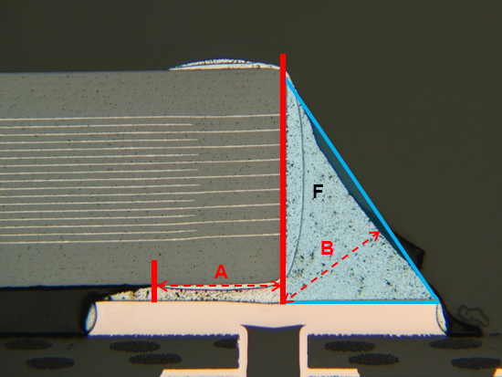
|
Crack length less than 60% of A+B,
|
|
chip capacitors
| |||
|
Cylindrical and square end-capped devices with cylindrical body
|
MELF
|
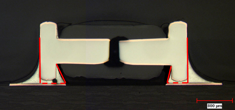
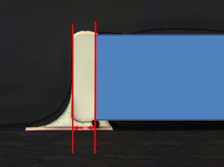 red line defines the critical zone |
Crack no longer than 33% of critical zone length
|
|
Bottom terminated chip device
|
SMD0.5, SMD1, SMD2, SMD0.2, SMD0.22
|
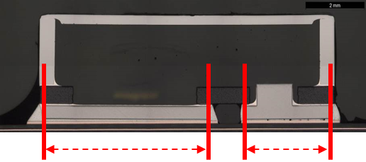
red line defines the critical zone |
No crack longer than 25% of lap connection
|
|
Castellated chip carrier device
|
LCCs
|
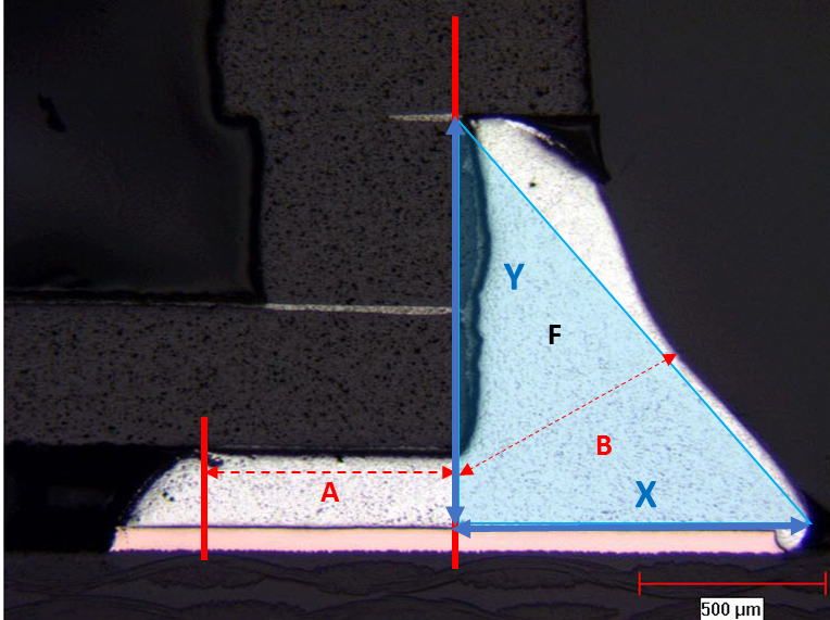
|
Crack length less than 70% of A+B
|
|
Flat pack and Gull-wing leaded device with round, rectangular , ribbon leads
|
SOT23
|
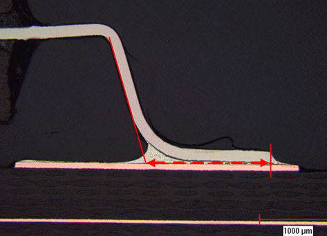
red line defines the critical zone |
Crack no longer than 33% of critical zone length
|
|
Specific case: TSOP
|
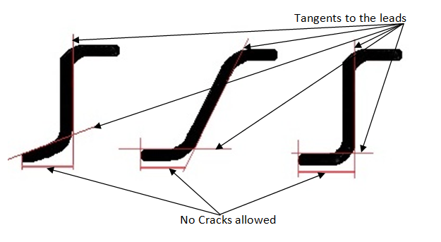
|
For TSOP no crack allowed in the critical zone
| |
|
Moulded magnetics
|
1553 interface transformers or specific transformers
|
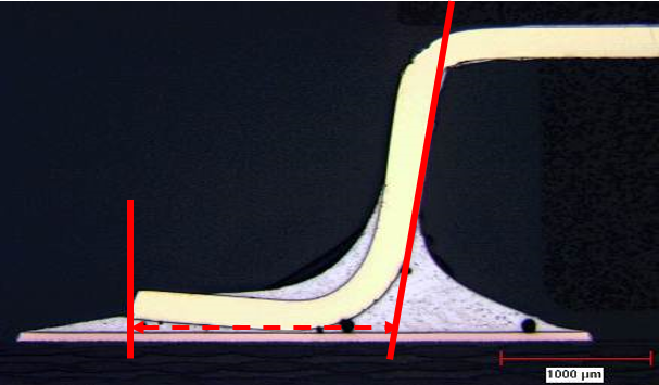
red line defines the critical zone |
Crack no longer than 33% of critical zone length
|
|
“J” leaded device
|
ceramic leaded chip carriers (CLCC) and plastic
|

red line defines the critical zone |
Crack no longer than 33% of critical zone length
|
|
Devices with ribbon terminals without stress relief (flat lug leads)
|
|
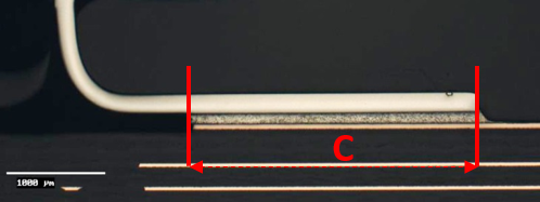
|
Crack no longer than 33% of critical zone length C
|
|
Device with Inward formed L-shaped leads
|
Tantalum chip capacitor
|
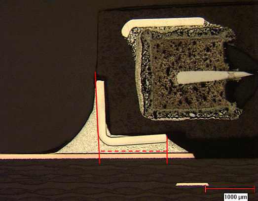
|
Crack no longer than 33% of critical zone length
|
|
Stacked modules devices with leads protruding vertically from bottom
|
|
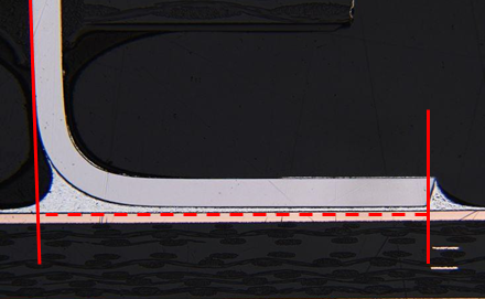
|
Crack no longer than 33% of critical zone length
|
|
Leaded device with plane termination
|
DPAK/TO252
|
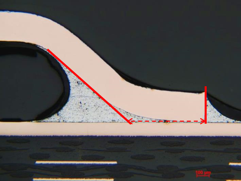
|
Crack no longer than 33% of critical zone length
|
Approval of verification
A letter confirming the completion of a successful verification programme shall be sent to the contact person of the supplier from the Approval Authority, with the SMT summary table specified in the DRD of Annex H attached to it.
- 1 The letter and the SMT summary table provide evidence of the verification approval to a third party.
- 2 The approval of verification applies to all space projects from the date of the approval until withdrawn.
- 3 The SMT summary table is prepared by the supplier and sent to the Approval Authority for approval.
<<deleted>>
<<deleted>>
Reference to the SMT summary table number shall be made on each space project declared processes list .
See ECSS-Q-ST-70, Table C-2.
Withdrawal of approval status
The approval status of the supplier shall be withdrawn when any of the following status justify its withdrawal:
- Repetitive supply problems and manufacturing defects.
- Undeclared changes to the PID.
- Continuous non-compliance with the PID.
Conditions for delta verification
The supplier shall undertake a verification for any new configuration not covered by similarity rules in accordance with requirements from clause 14.2.
The delta verification shall be performed when changes are undertaken as specified in Table 144.
For a process change verification programme based on assembly of already verified PCB materials, the choice of the PCB type or a sampling of several PCB types instead of all PCB materials may be selected, subject to agreement by Approval Authority.
- 1 The selection criteria is based on worst cases depending on the change of process to be verified.
- 2 Examples of worst cases are CTE mismatch, thermal dissipation, stiffness.
For delta-verification associated with process change the test vehicles shall be specified, in order to be representative of the process evolution.
The types and number of parts to be mounted on the test vehicles shall be specified as agreed by Approval Authority.
This allow to track any impact of the process evolution as defined in Table 144.
A delta-verification programme in accordance with the DRD from Annex G shall be submitted for approval to the Approval Authority.
Number of sensitive parts to be assembled and microsectioned shall be five.
Number of sensitive parts to be assembled and microsectioned may be reduced to three if the initial verification showed reproducible results.
Sensitive parts are from the ESCIES list and company PID.
Small size packages may be omitted from microsectioning providing that these package sizes are already in the company PID.
Table 144: Conditions invoking verification
|
Changes
|
Test vehicles without any test
|
Cleanliness tests
|
Material compatibility with cleaning solvent
|
Test vehicles with tests according to Figure 141, Figure 142 or Figure 143
|
|
New device mounting configuration (example, already verified with conformal coating and now mounted without)
|
|
|
|
x
|
|
New SMD package size
|
|
|
|
X
|
|
New manufacturer of passive chips
|
|
|
|
X
|
|
New material of printed circuit board
|
|
|
|
X
|
|
New thermal and/or mechanical adhesive
|
|
|
|
X
|
|
New conformal coating
|
|
|
|
X
|
|
New solder paste with same alloy, same powder size distribution, same flux activation type
|
X +microsections1
|
X
|
|
|
|
New solder paste with new alloy, flux activation type and/or different physical-chemical characteristics
|
|
|
|
X
|
|
New flux activation type for hand solder
|
X
|
X
|
|
|
|
New cleaning solvent and or new cleaning process
|
|
X
|
X
|
|
|
New reflow profile, Peak temp +/-5°C, duration above liquidus 2
|
|
|
|
X
|
|
New equipment to deposit soldering paste without change of process
|
X
|
|
|
|
|
New solder paste depositing process
|
|
|
|
X
|
|
New device placing equipment
|
X
|
|
|
|
|
New device placing equipment of same process method
|
Visual inspection only
|
|
|
|
|
New type of reflow equipment with process change
|
|
|
|
X
|
|
New reflow equipment without process change
|
X
|
|
|
|
|
Move Manufacture location outside the clean room approved in the PID
|
X
|
|
|
|
|
1 For microsection, one part per family type from the SMT summary table as per Annex H.
| ||||
Verification of cleanliness
The verification of the PCB cleanliness shall be performed for the following cases:
- for the first verification programme performed by a company,
- when the conditions of Table 144 request it. The cleanliness test of the board shall be conducted in accordance with requirements from the method 2.6.3.3 of IPC-TM-650 (2004).
Verification approval procedure
Request for verification
Verification approval procedure shall list the single point contact for all SMT matters.
RFA shall be issued.
The following items shall be submitted to the Approval Authority:
- A letter from the supplier signed by the contact person and the quality assurance organization of the supplier addressed to the Approval Authority, describing his experience in SMT and making the request for verification.
- One technology sample of SMT taken from the assembly line, to be verified, not carrying conformal coating for the Approval Authority to inspect.
Conformal coating to be omitted to enable detailed inspection to be undertaken by Approval Authority.
Technology sample
The technology sample shall be inspected by the Approval Authority in accordance with the requirements from clause 13.
The qualifying authority may waive the need for technology sample.
Audit of assembly processing
The Approval Authority shall inform the supplier on the result of inspection of a technology sample specified in the requirement 14.15.2a.
The Approval Authority shall inform the supplier on acceptance regarding the start of the next stages of the approval process.
The audit of the supplier’s assembly line shall be performed prior to verification programme.
Guidelines to audit report is given in Annex D.
The findings of the audit shall remain confidential between Approval Authority and the supplier.
Verification programme
A verification programme shall be submitted to the Approval Authority for acceptance prior to the start of assembly of the test SMT in accordance with DRD from Annex G.
Final verification review
The verification test report shall contain the following information:
- Applicable documents for verification
- Manufacturing traveller including devices traceability
- Vibration profile and responses
- Shock input if applicable
- Thermal cycle
- Visual inspection and MIP reports
- Microsection
- Nonconformances reports. The verification test report shall be made available to the Approval Authority.
Certification approval of assembly line
Following the completion of the final verification review, the following documents shall be submitted to the Approval Authority for approval:
- PID
- SMT summary tables.
Assembly line audit shall be conducted every four years by the Approval Authority.
In case of changes in assembly line, impacting its approval an early audit shall be conducted to re-establish the approval as specified in the requirement 14.15.6b.
Quality assurance
General
Requirements from clause 5 from ECSSQST20 shall apply for "Quality assurance".
Data
Requirements from clause 14.2 from ECSSQST7008 shall apply for "Data".
Nonconformance
The requirements from clauses 5 and 6 from ECSSQST10-09 shall apply for "Nonconformance".
Calibration
Requirements from clause 14.4 from ECSSQST7008 shall apply for "Calibration".
Traceability
Requirements from clause 14.5 from ECSSQST7008 shall apply for "Traceability".
Workmanship standards
<<deleted>>
Visual standards consisting of work samples or visual aids that illustrate the quality characteristics of all soldered connections involved shall be prepared and be available to each operator and inspector.
The illustrations presented in Annex I of this Standard can be included as part of the examples.
Inspection
During all stages of the process, the inspection points defined in the manufacturing flow chart shall be carried out.
The inspection shall be performed in conformance with clause 13 of this Standard.
<<deleted>>
Operator and inspector training and certification
Requirements from clause 18.8 from ECSSQST7008 shall apply for "Operator and inspector training and certification".
A training programme for operators and inspectors performing all processes contained within the PID shall be developed, maintained and implemented by the supplier to provide excellence of workmanship and personal skill in SMTs.
Records of training, testing and certification status of the operators are maintained for at least 10 years.
Operators and inspectors shall be trained and certified at a school or in-house training authorised by the Approval Authority.
The operators performing X-ray inspection shall be trained and in-house certified to perform and assess X-ray results.
Quality records
<<deleted, requirement modified in 15.9d>>
<<deleted, requirement modified in 15.9d>>
<<deleted, requirement modified in 15.9d>>
<<deleted, requirement modified in 15.9d>>
The following documents, as a minimum, shall be made available:
- PID,
- Audit report established by the Approval Authority,
- Verification report.
<<deleted and moved into clause 14.7.2 and Annex I>>
ANNEX(informative)<<deleted>>
ANNEX(informative)<<deleted, SMT summary table DRD created in Annex H>>
ANNEX(informative)<<deleted>>
ANNEX(informative)Example of an SMT audit report
ECSS-Q-ST-70-38: SURFACE MOUNT TECHNOLOGY PROCESS AUDIT REPORT
|
SECTION 1 |
COMPANY DETAILS |
||||
|
1. NAME |
|
||||
|
2. ADDRESS |
|
||||
|
3. TEL |
|
||||
|
4. FAX |
|
||||
|
5. MANAGING DIRECTOR |
|
||||
|
6. QUALITY MANAGER |
|
||||
|
7. PRODUCTION MANAGER |
|
||||
|
8. SMT CONTACT PERSON |
|
||||
|
9. SMT PRODUCT RANGE AND HISTORY (brief summary) |
|
||||
|
10. Numbers of SMT operators |
|
Design Engineers |
|
QA |
|
ECSS-Q-ST-70-38: SURFACE MOUNT TECHNOLOGY PROCESS AUDIT REPORT
|
SECTION 2 |
QUALITY SYSTEM |
|||||
|
1. QUALITY MANUAL* Reference: |
|
|||||
|
Issue: |
|
|||||
|
Date: |
|
Viewed |
Y N |
|||
|
2. ORGANISATION OF THE QUALITY DEPARTMENT FOR SMT |
|
|||||
|
3. INTERNAL QUALITY AUDIT SYSTEM Reference: |
|
|||||
|
Date of last audit: |
|
|||||
|
Comments: |
|
Viewed |
Y N |
|||
|
4. NON-CONFORMANCE SYSTEM Reference: |
|
|||||
|
|
No. of NCRs in previous 12 months: |
|
No. open at audit date: |
|
Viewed |
Y N |
|
5. CURRENT QUALITY APPROVALS Date of last assessment |
|
|||||
|
6. COMMENT ON COMMITMENT TO ECSS-Q-ST-70-38 |
|
|||||
|
7. REFERENCE TO GENERAL ESA AUDIT & Date |
|
|||||
- Note: Request that a copy of the Contents List of the Quality Manual be appended to this report (See Attachment 1).
ECSS-Q-ST-70-38: SURFACE MOUNT TECHNOLOGY PROCESS AUDIT REPORT
|
SECTION 3 |
PROCESS CONTROL |
|
1. SMT APPROVED (if any) Make reference to an existing list of SMT configurations considered already tested. Identify how the SMT was tested. |
|
|
2. Make reference to the procedures that have the following functions and identify current issue and date: |
|||
|
Process Identification Document |
|
||
|
1. Process instructions |
|
||
|
|
|
Viewed: |
Y N |
|
2. Workmanship acceptance/rejection criteria |
|
||
|
|
|
Viewed: |
Y N |
|
3. Calibration of SMT tooling |
|
||
|
|
Viewed: |
Y N |
|
|
4. Control of limited Shelf life materials |
|
||
|
|
|
Viewed: |
Y N |
|
5. Material procurement control with CofC or CofTest |
|
||
|
|
Viewed: |
Y N |
|
|
3. TRAINING Make reference to the procedure for operator and inspector training. Identify the number of certificated operators and inspectors. |
|
|||
|
|
Viewed: |
Y N |
Certificates viewed: |
Y N |
ECSS-Q-ST-70-38: SURFACE MOUNT TECHNOLOGY PROCESS AUDIT REPORT
|
SECTION 4 |
FACILITIES |
|
CHECK LIST |
|
|
Devices storage and kitting area. |
|
|
Humidity and temperature control |
|
|
ESD protection and control |
|
|
Cleanliness in assembly areas |
|
|
Calibration |
ESD (floor, mat, chair, wrist, solder iron….): |
|
Degolding, pretinning bath: |
|
|
Lead forming: |
|
|
Machine reflow: |
|
|
Solder tip: |
|
|
Repair station: |
|
|
Ovens: |
|
|
Lighting in Lux |
Degolding: |
|
Pretinning: |
|
|
Lead forming: |
|
|
HS Assembly: |
|
|
Stacking, bonding: |
|
|
Conformal coating: |
|
|
PCB drying ovens and procedure |
Unpopulated: |
|
Populated without conformal coating: |
|
|
Populated with conformal coating: |
|
|
Oven |
Baking of naked PCB: |
|
Baking of populated PCB: |
|
|
Curing of adhesive: |
|
|
Curing of conformal coating: |
|
|
Repair prior conformal coating |
|
|
Repair after conformal coating: |
|
|
Bending tools |
|
|
Magnification aids |
Device preparation (degolding, pretinning, lead forming): |
|
After solder paste application: |
|
|
After assembly by machine reflow: |
|
|
During assembly by hand: |
|
|
Final inspection: |
|
|
Degolding bath (250C-280C) |
|
|
Pretinning (210-260C) |
|
|
Solder fluxes (internal and external) used. Flux activity and trademark. |
Degolding, pretinning: |
|
Solder paste: |
|
|
Hand soldering: |
|
|
Cleaning Solvents |
PCB cleaning: |
|
Degolding, pretinning: |
|
|
Soldering by machine reflow: |
|
|
Solder screen |
|
|
Soldering by hand: |
|
|
Prior to bonding, stacking: |
|
|
Prior to conformal coating: |
|
|
Solder alloys (chemical composition, supplier, trademark and associated flux |
-Dispensing: |
|
Screen printing: |
|
|
HS: |
|
|
Solder paste application |
Stencil: |
|
Dispensing: |
|
|
Repair station: |
|
|
Pick and place machine |
|
|
Machine reflow |
|
|
Is the soldering equipment well controlled (temperature-time profile, speed control…). How is the temperature profile controlled on the FM? |
Machine reflow: |
|
Solder Iron: |
|
|
Hand Soldering iron (280C to 340C max) |
|
|
Fume exhaust facilities |
|
|
Repair station |
|
|
Cleaning Equipment |
Machine reflow |
|
Hand soldering: |
|
|
Cleanliness Testing (< 1,6 g/cm2) |
|
|
Stacking , bonding compounds |
|
|
Refrigerators: check expiration dates for adhesives, conformal coatings |
Solder paste: |
|
Adhesive: |
|
|
Conformal coating: |
|
|
Conformal Coating used |
Curing conditions: |
|
Cleanliness in conformal coating facilities |
|
|
Areas for Non-Conforming Items (Quarantine) |
|
|
Laboratories exist for: - Temperature cycling - Vibration - Electrical testing - Microsectioning |
|
|
SMT Assembly Traveller (operator activities, inspector stamps) |
|
END OF SECTION 4ECSS-Q-ST-70-38: SURFACE MOUNT TECHNOLOGY PROCESS AUDIT REPORT
|
SECTION 5 |
FINAL ASSESSMENT |
An assessment of the surface mount technology line at the following suppliers facility has been undertaken and the following conclusions made:Supplier: Address: THE FACILITIES FOR THE ASSEMBLY OF SURFACE MOUNT TECHNOLOGY (ACCORDING TO ECCS-Q-ST-70-38C AT THE ABOVE SUPPLIER’S SITE ARE CONSIDERED:SUITABLE CONDITIONALLY SUITABLE NOT SUITABLESUMMARY OF FINDINGS/CONDITIONS OF APPROVAL/SUMMARY OF CORRECTIVE ACTIONS NECESSARY:
|
Actions |
Findings |
Due date |
NAME SIGNPROCESS ASSESSMENT CARRIED OUT BY (Approval Authority): IN PRESENCE OF (CONTRACTOR): DATE:Approval Authority: DATE: END OF DOCUMENT
ANNEX(informative)Additional information
<<deleted>>
<<deleted>>
Melting temperatures and choice
Table: Guide for choice of solder type
|
Solder type
|
Melting range (C)
|
Uses
| |
|
|
Solidus
|
Liquidus
|
|
|
63 tin solder (eutectic)
|
183
|
183
|
Soldering printed circuit boards where temperature limitations are critical and in applications with an extremely short melting range. Preferred solder for surface mount devices.
|
|
62 tin silver loaded
|
179
|
190
|
Soldering of terminations having silver and or silver palladium metallization. This solder composition decreases the scavenging of silver surfaces.
|
|
60 tin solder
|
183
|
188
|
Soldering electrical wire/cable harnesses or terminal connections and for coating or pretinning metals.
|
|
96 tin silver (eutectic)
|
221
|
221
|
Can be used for special applications, such as soldering terminal posts.
|
|
75 indium lead
|
145
|
162
|
Special solder used for low temperature soldering process when soldering gold and gold-plated finishes. Can be used for cryogenic applications.
|
|
70 indium lead
|
165
|
175
|
For use when soldering gold and gold-plated finishes when impractical to degold.
|
|
50 indium lead
|
184
|
210
|
This solder has low gold leaching characteristic.
|
|
10 tin lead
|
268
|
290
|
For use in step-soldering operations where the initial solder joint must not be reflowed on making the second joint (e.g. CGA columns, connections internal to devices)
|
ANNEX(normative)Process Identification Document (PID) - DRD
DRD identification
Requirement identification and source document
This DRD is called from ECSS-Q-ST-70-38, requirement 5.1.2a.
Purpose and objective
The purpose of the PID is to consolidate the overall management, process and facilities utilised during the manufacturing and verification of the SMD.
Expected response
Scope and content
SECTION 1: Document format
The PID shall contain the following information about the Document Format:
- Cover page: document title, document reference, revision number and date, page numbering, signing of Production and Quality representatives,
- Follow-up of PID updates: registration of PID updates indicating the nature of the update and the sections and pages updated,
- Purpose and scope of the document,
- Table of contents. SECTION 2: Manufacturing control
The PID shall contain the Manufacturing control flow chart of the verified SMT.
- 1 This illustrates the various stages of procurement, manufacturing and inspection operations specific to this technology in a flow chart format.
- 2 It can be used to identify, among others:
- the operation,
- the body responsible for its implementation,
- related documents: (only their reference),
- procurement specifications (for materials),
- acceptance inspection procedures (for materials and devices),
- manufacturing procedures,
- manufacturing and quality control procedures during and at the end of production.
SECTION 3: Specifications
The PID shall contain the following information about Specifications:
- List of procurement specifications, assembly procedures and inspection procedures concerning the technology dealt within the PID, including the precise title, the reference or number, the revision number and date of each document,
- Printed circuit design rules in compliance with requirements from ECSS-Q-ST-70-12,
- General Quality Assurance documents relating to the technology. SECTION 4: Organisation
The PID shall contain the following information about Organisation:
- Represented as a flow chart: organization of the company, organization of production department and organization of the quality Department,
- Focal point and PID responsible,
- Operators and inspectors’ certification methodology. SECTION 5: Manufacturing traveller or log file
The PID shall contain as a minimum the following information about the Manufacturing traveller or log file:
- The sequencing of the various operations in their logical order of execution,
- The references of the documents referred to and used during these operations,
- The references of the Quality documents to ensure traceability of the various batches of material used (record reference), together with the work stations and tools employed,
- The signatures of the various actors with the date on which the task was completed. Section 6: List of verified technology
The PID shall contain as a minimum the following information about the List of verified technology:
- List of materials,
- Temperature and time profiles for the machine reflow used in the verification,
- List of verified devices per assembly configuration,
- List of sensitive devices,
- List of devices with limited project verification. SECTION 7: Description of production line
The PID shall contain as a minimum the following about the Description of production line:
- Layout of premises with associated surface area, with indication of location of production machines and quality inspection,
- Working environment; cleanliness class, ambient temperature limits, humidity and positive pressure limits for each type of activities. SECTION 8: List of equipment
The PID shall contain a list of all machines and tools utilised during the SMT activity.
SECTION 9: List of laboratory services
The PID shall contain range and capability of supporting laboratory services.
SECTION 10: Project SMT heritage
The PID shall contain a of board SMT assembly by year manufactured in accordance with the PID.
Special remarks
None.
ANNEX(normative)Verification programme report - DRD
DRD identification
Requirement identification and source document
This DRD is called from ECSS-Q-ST-70-38, requirement 14.1a.
Purpose and objective
The purpose of the Verification programme report DRD is to detail the requirements for the documentation of the verification programme.### Expected response
Scope and content
The verification programme documentation shall contain as a minimum the following:
- Indication of method of the assembly:
- The soldering method and repair methods
- PCB information:
- PCB material and manufacturer
- PCB footprint surface finish
- Number of layers
- Thickness
- Built up with identification of signal and full copper plane
- Connection of the footprints to the internal layer representative of the FM
- Location of the devices on the PCB
- Location of the mechanical fixation or stiffeners if any
- Number of PCB used for the verification programme.
- Materials used
- Solder paste and wire designation, commercial trade mark, and composition with associated flux class
- Flux class used for pretinning and soldering
- Conformal coating
- Adhesive for mechanical, and for thermal
- Solvent
- Others.
- List of devices
- Environmental test conditions and facility
- Verification method Microsection or Electrical monitoring
- Microsection laboratory
- PID and Manufacturing document process references
- Verification workflow
- Verification by similarity
- NCRs
- Certification status of the operators and inspectors
- Compliance status of the operators and inspectors
- Compliance of the manufacturing room
- Additional information.
to item 1.(a): When machine reflow is used then the verified hand soldering or other method is used.
The content of documentation specified in G.2.1a.1 to 13 may be tailored for companies having already an ECSS SMT approval.
Special remarks
None.
ANNEX(normative)SMT summary table - DRD
DRD identification
Requirement identification and source document
This DRD is called from ECSS-Q-ST-70-38, requirement 14.11a.
Purpose and objective
The purpose of the SMT summary table is to consolidate the approval status of the boundary conditions for the verification activity.
Expected response
Scope and content
The SMT summary table shall include the following data
- Assembly processes
- PID reference with issue
- Solder type: For machine reflow and for hand assembly
- Conformal coating
- Substrate type: Polyimide
- Device data as shown in Table H-1.
Examples of assembly processes are vapour phase and hand soldering or convection reflow + hand soldering or hand soldering.
Special remarks
None.
Table: Device type preparation and mounting configuration
|
Device family
|
Package
|
Manufacturer
|
Package dimensions
|
Bonding material (under device)
|
Stacking material (edge or corner)
|
Terminal material
|
Lead finish
|
Pitch
|
Nominal Terminal thickness (mm)/ Nominal width
|
In-House degolding / pretinning
|
In-house lead forming
|
Artificial stand-off
|
Final report
|
|
Ceramic chip
|
C0603 Type 1
|
|
Length, width
|
NA
|
NA
|
|
Sn/Pb
|
NA
|
NA
|
No
|
N/A |
No |
|
|
Ceramic
|
C0603 Type 11
|
|
|
|
|
|
|
|
|
|
N/A |
|
|
|
Ceramic resistor
|
R0805
|
|
|
NA
|
NA
|
|
Sn/Pb
|
NA
|
NA
|
No
|
N/A |
No |
|
|
Diode
|
D5-B
|
|
|
|
|
|
|
|
|
|
N/A |
|
|
|
Tantalum capacitors
|
|
|
|
|
|
|
|
|
|
|
|
|
|
|
IC
|
FP10 Bottom brazed
|
|
|
yes
|
One the side
|
Alloy42
|
Gold
|
1,27
|
0,25
|
yes
|
yes |
NA |
|
|
CQFP
|
CQFP196 top brazed
|
|
|
|
|
Kovar
|
|
|
|
|
No |
|
|
ANNEX(informative)Visual and X-ray workmanship standards
Workmanship illustrations for standard SMDs
Chip components
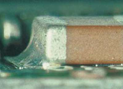 Figure: Preferred solder (see also Table 111)
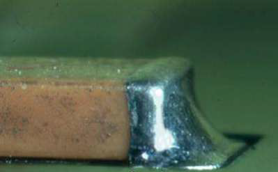 Figure: Acceptable, maximum solder (see also Table 111)
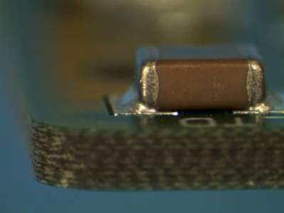 Figure: Acceptable, minimum Solder (see also Table 111)
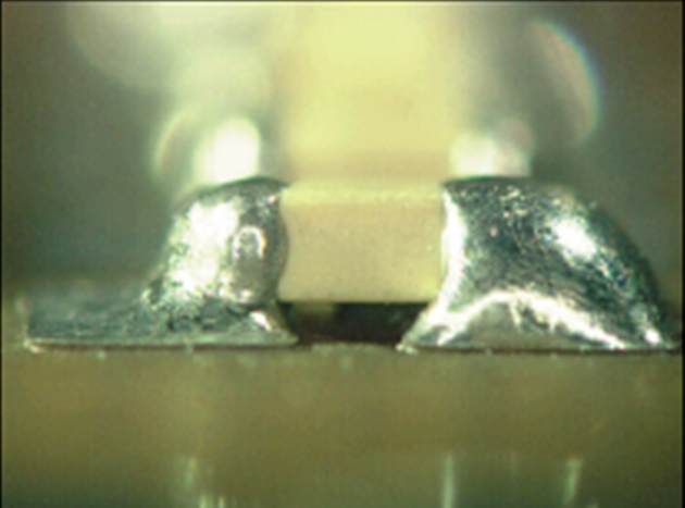 Figure: Unacceptable, excessive solder (see also Table 111)
 Figure: Unacceptable, poor wetting (see also Table 111)
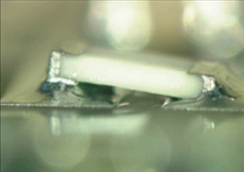 Figure: Unacceptable, excessive tilt (see also Table 111)
 Figure: Unacceptable, tombstone effect
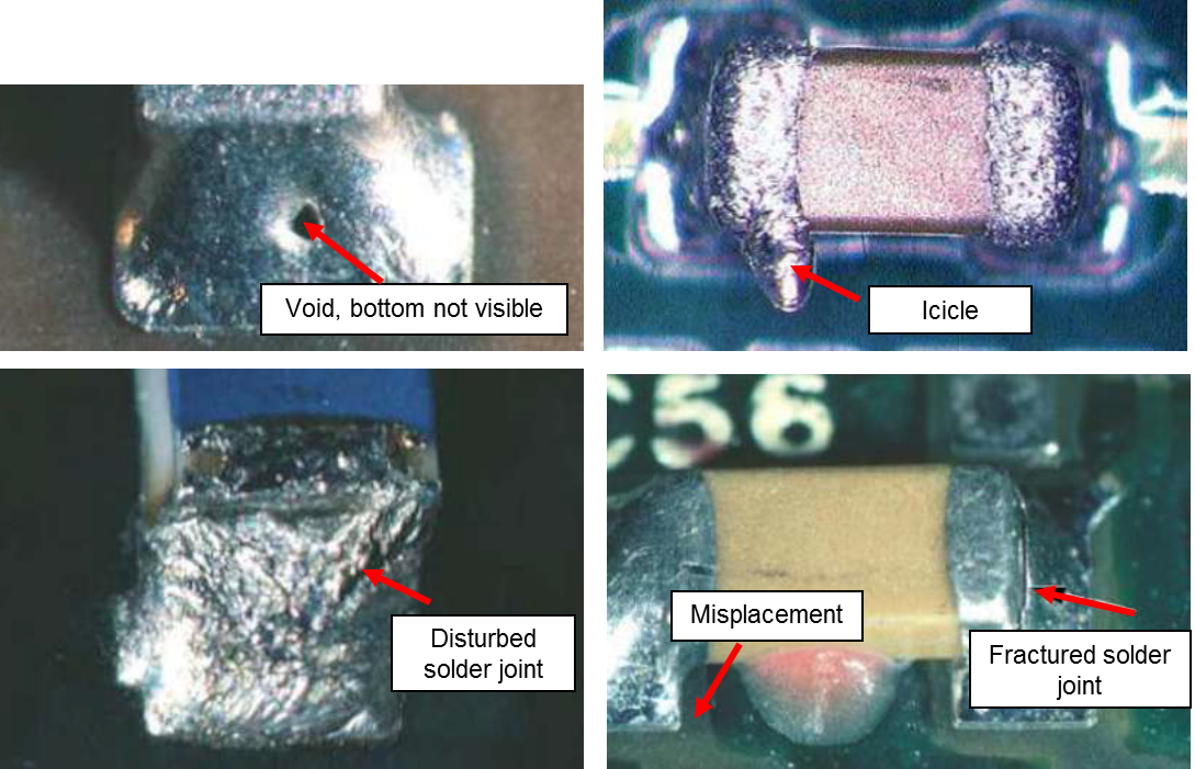 Figure: Examples of Unacceptable solder joints - (see also Table 111)
MELF components
 Figure: Acceptable, terminal wetted along end, face and sides (see also Table 111)
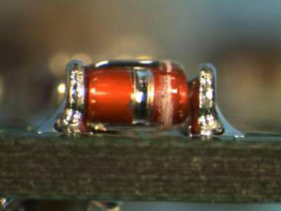 Figure: Acceptable, maximum solder joint (see also Table 113)
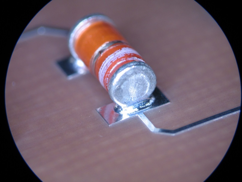 Figure: Not Acceptable, insufficient solder joint (see also Table 113)
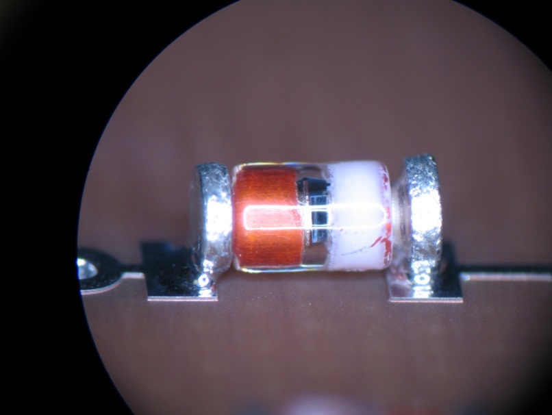 Figure: Unacceptable overhang
Gull-wing leaded devices with round, rectangular, ribbon shape

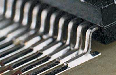 Figure: Examples of Gullwing leads: Acceptable
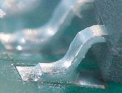 Figure: Examples of gull-wing device with rectangular lead: Acceptable
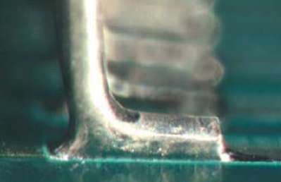 Figure: Acceptable, minimum solder joint
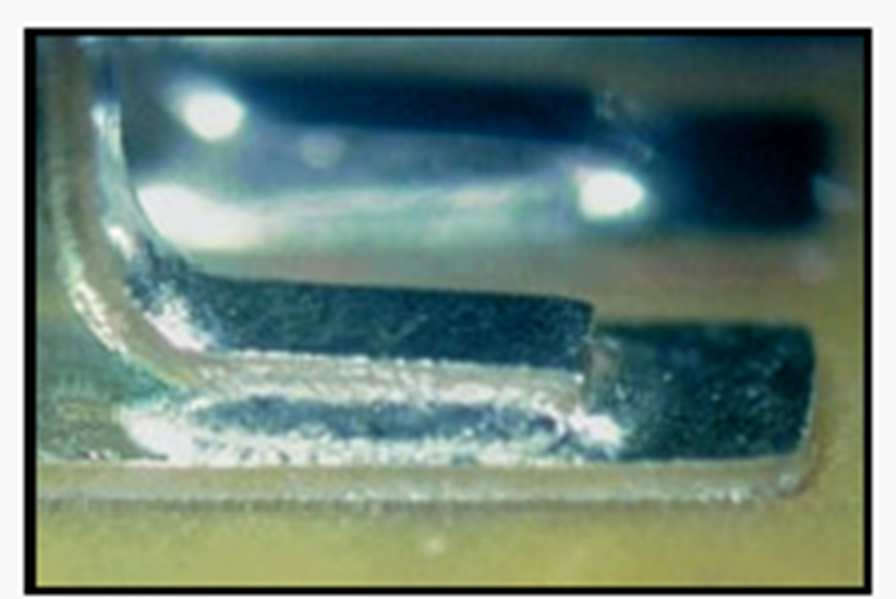 Figure: Unacceptable, insufficient heel fillet
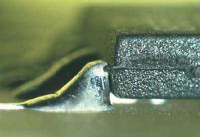 Figure: Unacceptable, excessive solder
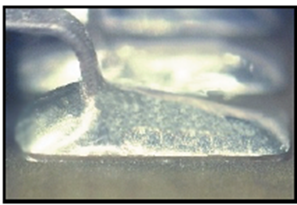 Figure: Unacceptable, excessive solder
“J” leaded devices
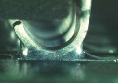 Figure: Preferred solder joint
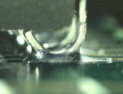 Figure: Acceptable solder joint
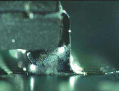 Figure: Unacceptable, excessive solder joint
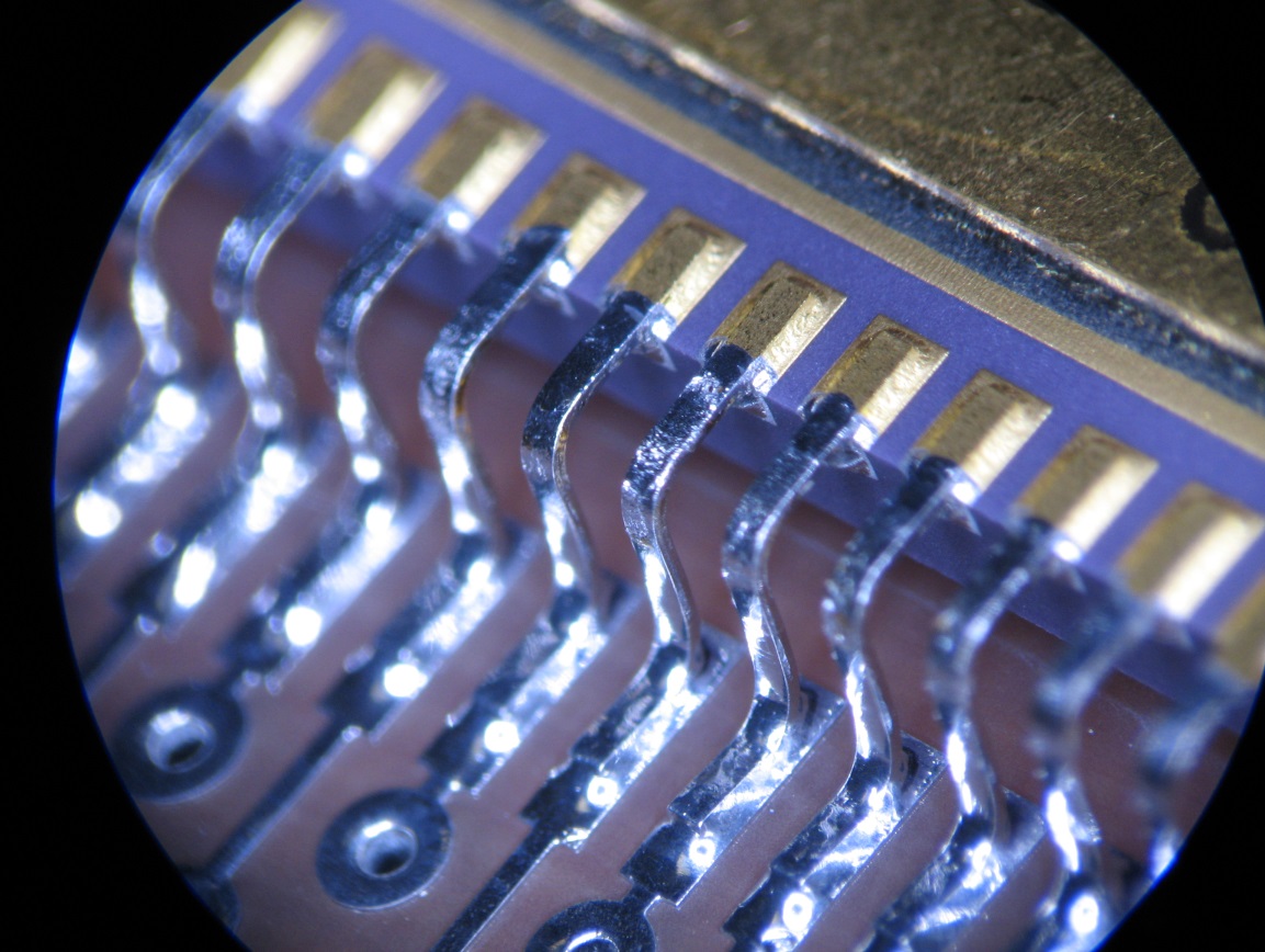 Figure: Unacceptable, excessive degolding
L-shape Inward leaded component
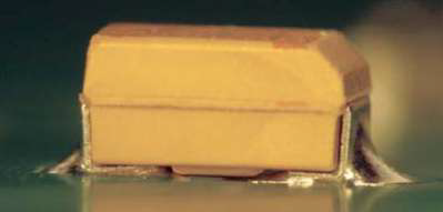 Figure: Acceptable, preferred solder joint
LCC devices
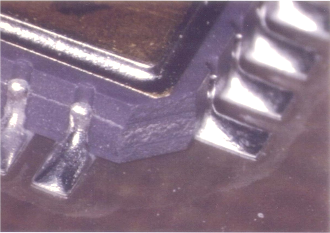 Figure: LCC General view, acceptable solder joints
Miscellaneous soldering defects
Figure: Examples of unacceptable soldering
Workmanship illustrations for ball grid array devices
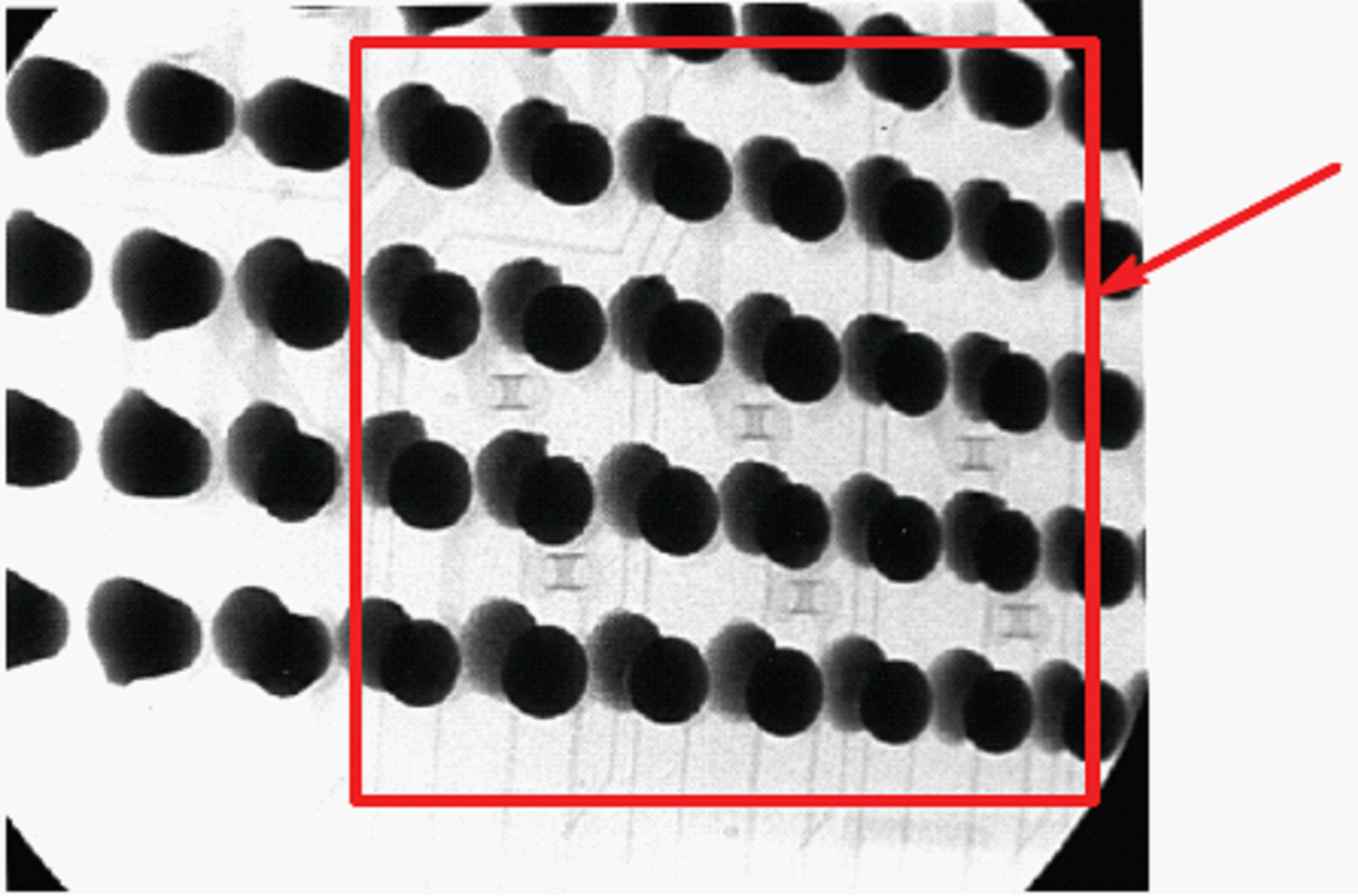 Figure: Angled-transmission X-radiograph showing solder paste shadow due to partial reflow: Reject
 Figure: Micrograph showing
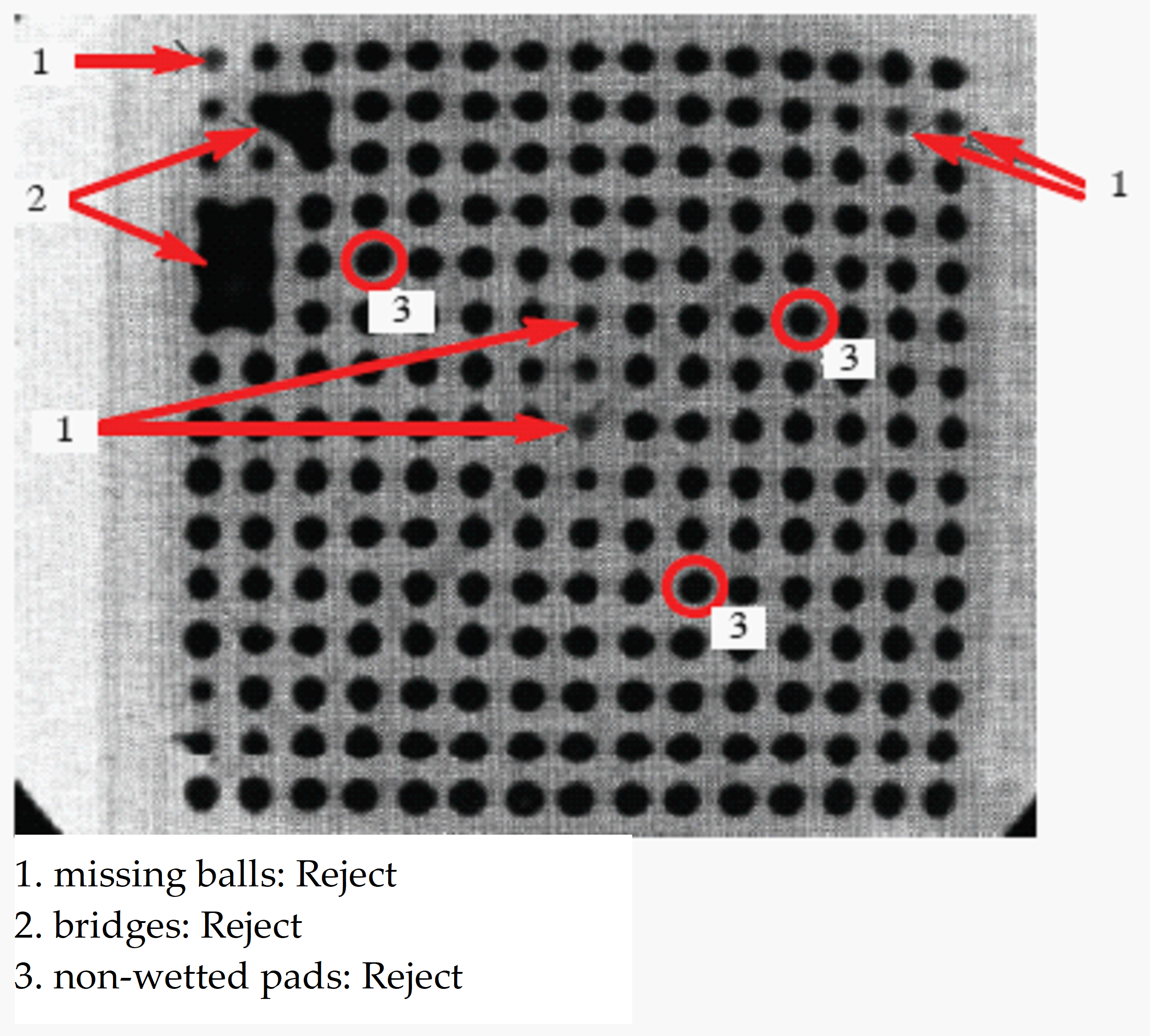 Figure: Perpendicular transmission X-radiograph showing unacceptable defects
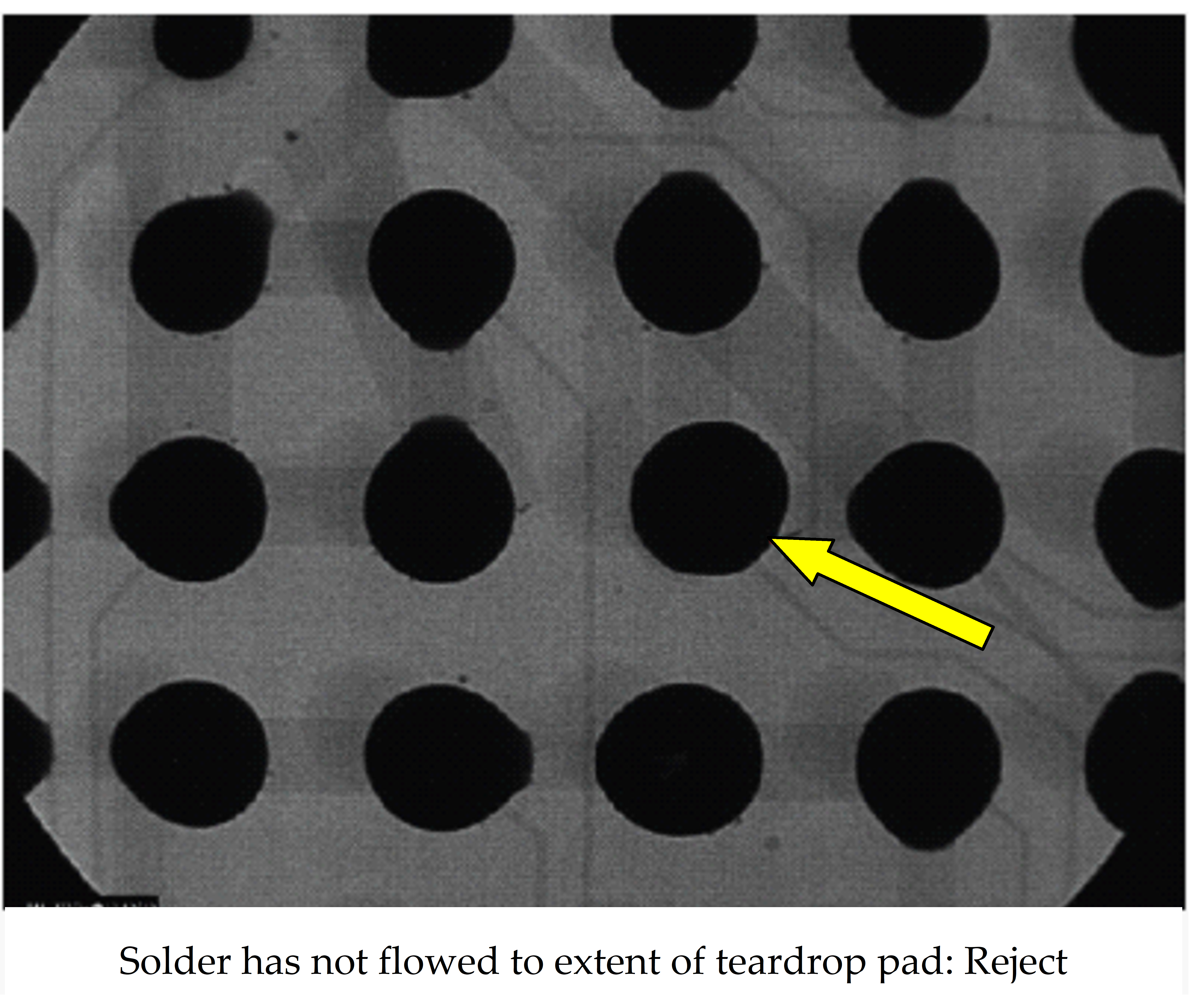 Figure: Perpendicular transmission X-radiograph showing non-wetted footprint
Workmanship illustrations for column grid array devices
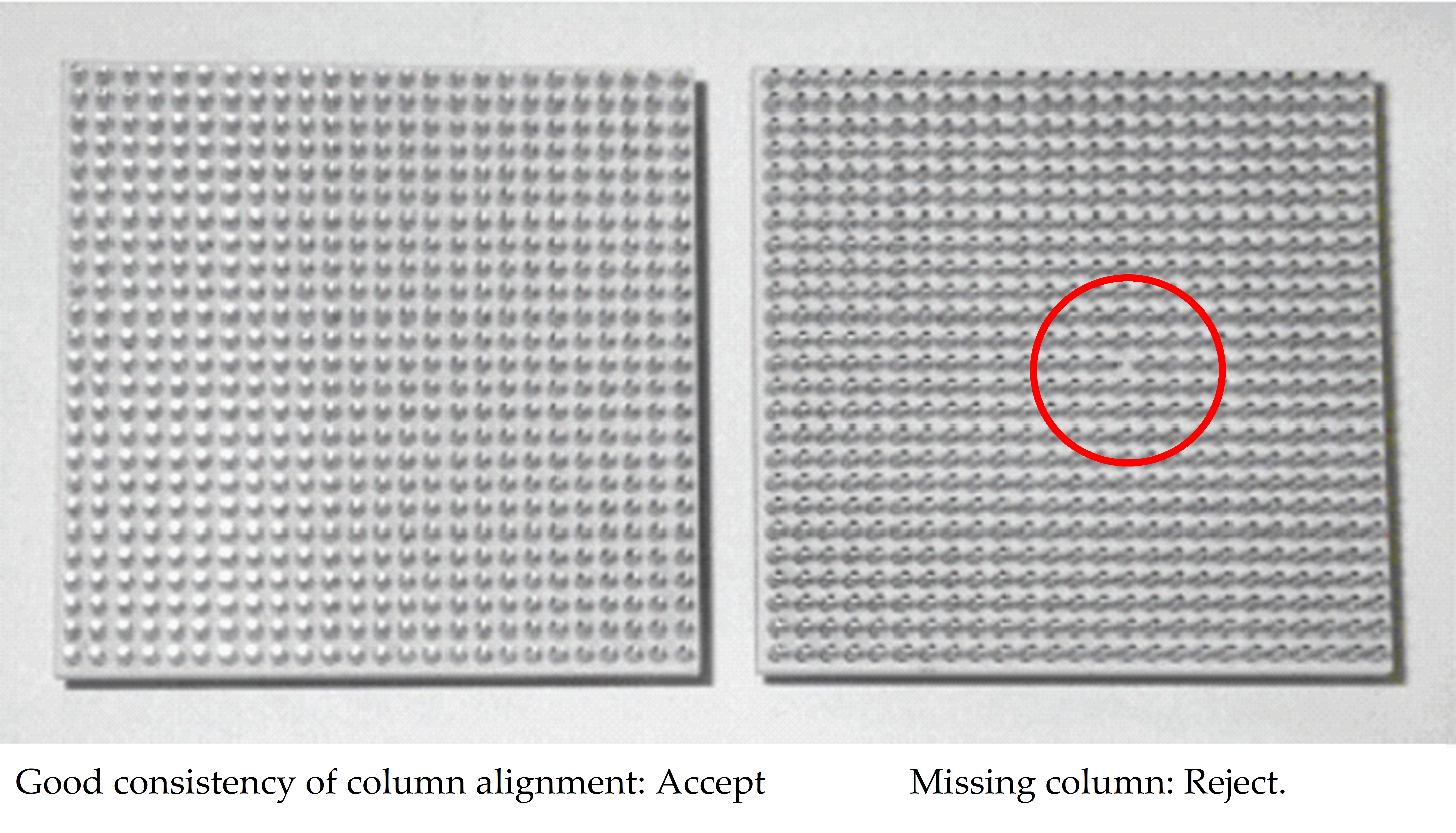 Figure: Underside view showing missing column
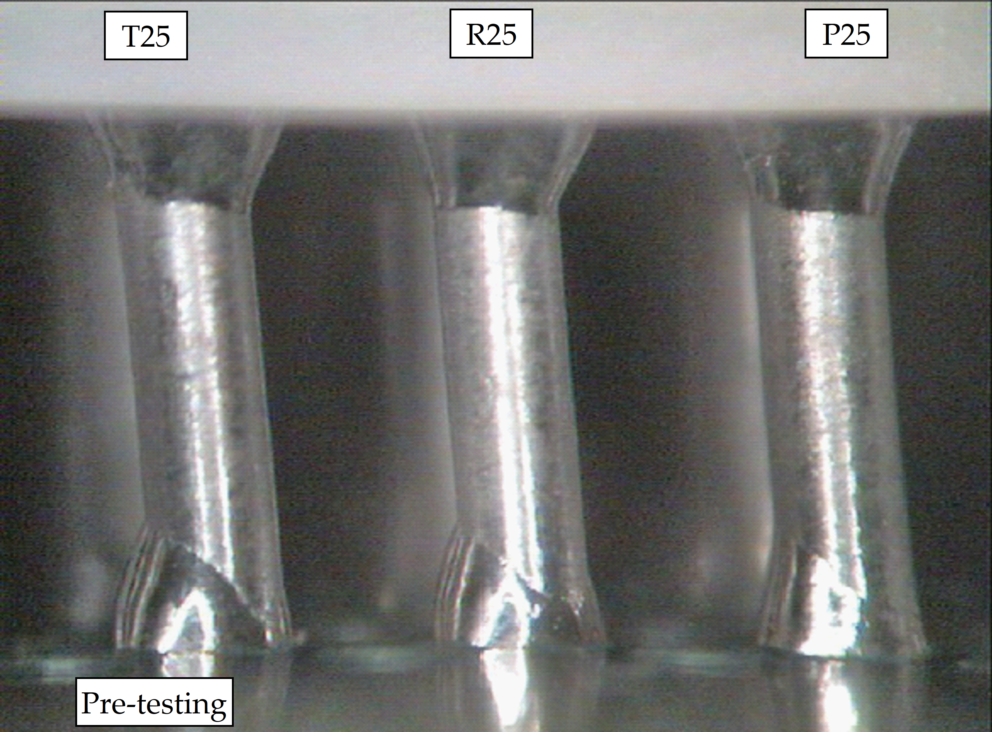 NOTE: Asymmetry of solder fillets at PCB is consequence of teardrop footprints and is acceptable
Figure: CGA mounted on PCB showing columns tilted < 10°: Accept
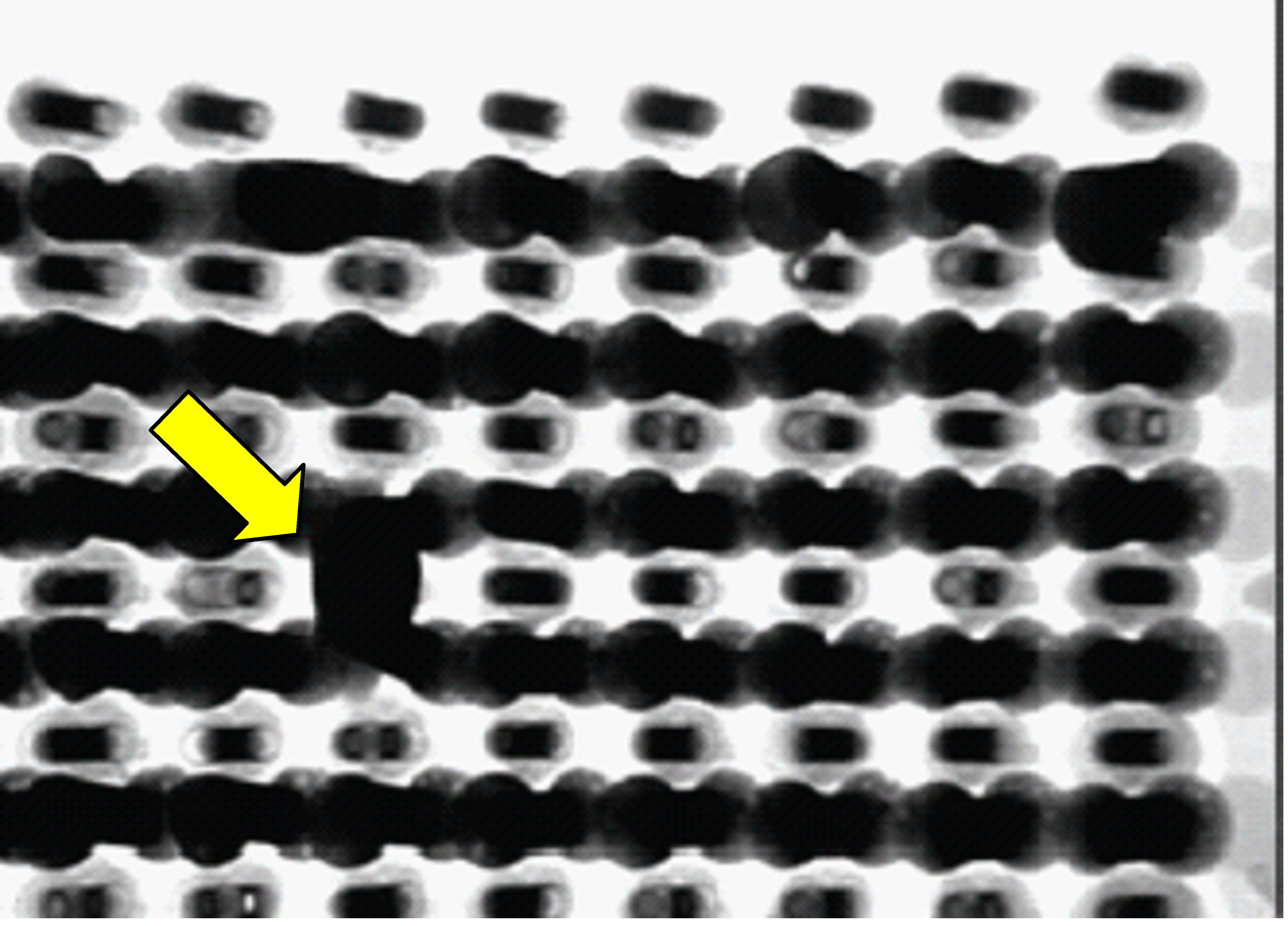 Figure: X-radiograph of CGA mounted on PCB showing solder bridge: Reject
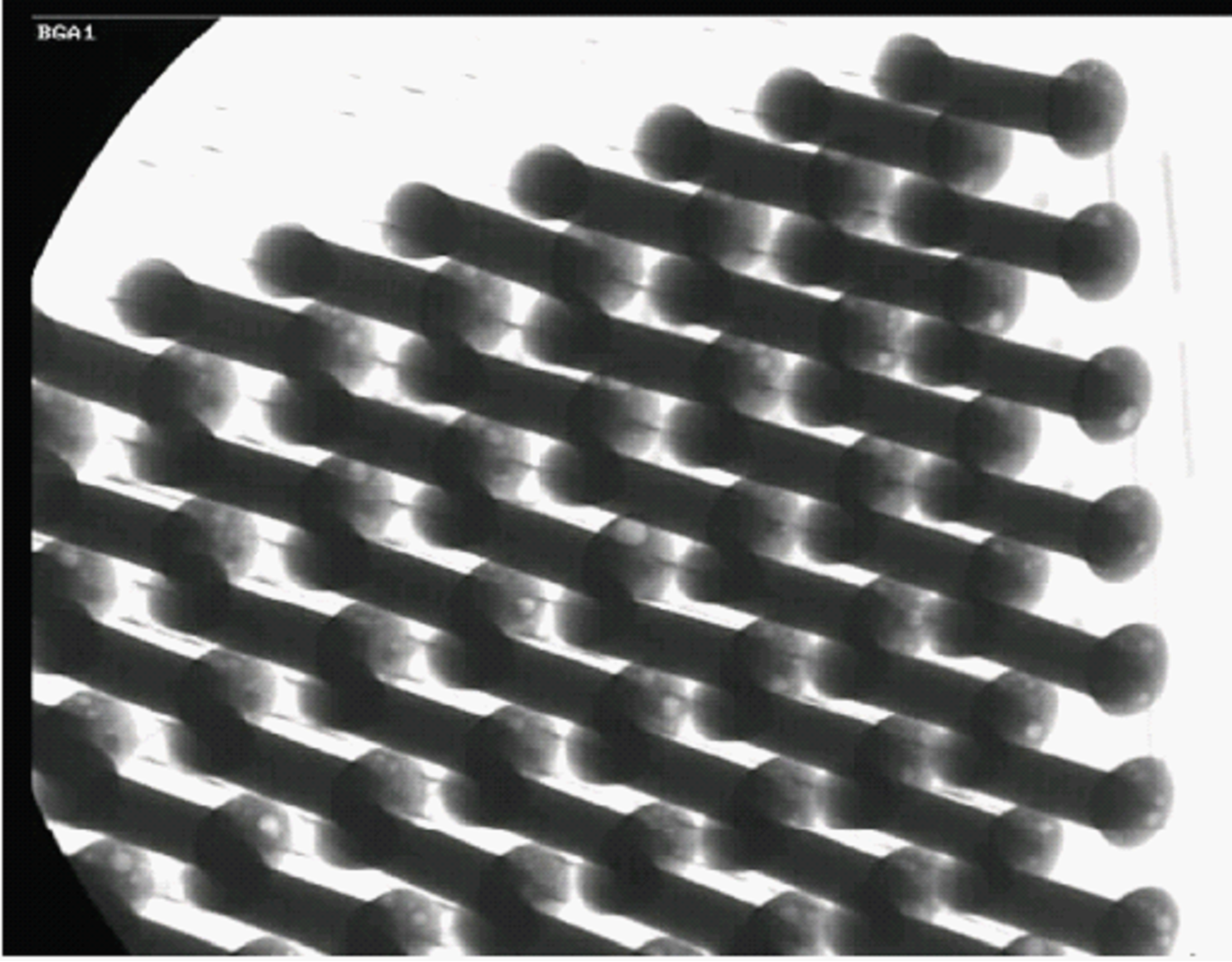 Figure: X-radiograph of CGA showing solder fillets at base of columns: acceptable
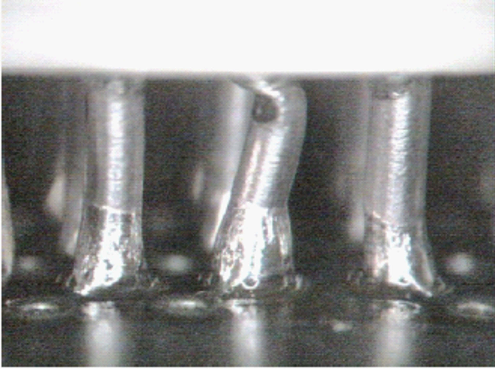 Figure: Micrograph of CGA mounted on PCB, bent column: reject
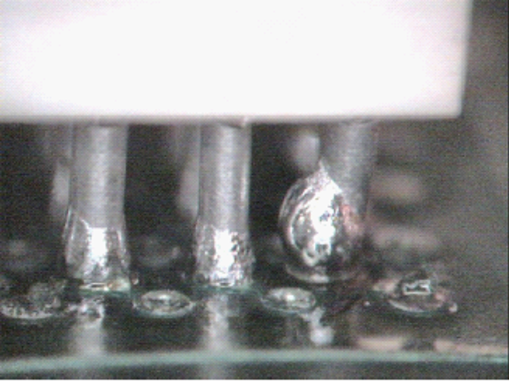 Unsoldered column: Reject.
Figure: Micrograph of CGA mounted on PCB
Bibliography
|
ESA STM-265, August 2001
|
Evaluation of Thermally Conductive Adhesives during the Assembly of Spacecraft Electronics.
|
|
ESA SP-1173 August 1994
|
Evaluation of Conformal Coating for Future Spacecraft Application s.
|
|
ECSS-E-ST-10-03
|
Space engineering - Testing.
|
|
ECSS-E-HB-20-05
|
Space engineering - High voltage engineering and design handbook
|
|
ECSS-E-HB-32-25
|
Space engineering - Mechanical shock design and verification handbook
|
|
ECSS-S-ST-00
|
ECSS System - Description, implementation and general requirements
|
|
EN 61190-1-1:2002
|
Attachment materials for electronic assembly - Part 1-1: Requirements for soldering fluxes for high-quality interconnections in electronics assembly
|
|
EN 61190-1-2:2014
|
Attachment materials for electronic assembly - Part 1-2: Requirements for soldering pastes for high-quality interconnects in electronics assembly
|
|
EN 61190-1-3:2007+A1:2010
|
Attachment materials for electronic assembly - Part 1-3: Requirements for electronic grade solder alloys and fluxed and non-fluxed solid solders for electronic soldering applications
|