
Space product assurance
Generic procurement requirements for hybrids
Foreword
This Standard is one of the series of ECSS Standards intended to be applied together for the management, engineering and product assurance in space projects and applications. ECSS is a cooperative effort of the European Space Agency, national space agencies and European industry associations for the purpose of developing and maintaining common standards. Requirements in this Standard are defined in terms of what shall be accomplished, rather than in terms of how to organize and perform the necessary work. This allows existing organizational structures and methods to be applied where they are effective, and for the structures and methods to evolve as necessary without rewriting the standards.
This Standard has been prepared by the ECSS-Q-ST-60-05 Working Group, reviewed by the ECSS Executive Secretariat and approved by the ECSS Technical Authority.
Disclaimer
ECSS does not provide any warranty whatsoever, whether expressed, implied, or statutory, including, but not limited to, any warranty of merchantability or fitness for a particular purpose or any warranty that the contents of the item are error-free. In no respect shall ECSS incur any liability for any damages, including, but not limited to, direct, indirect, special, or consequential damages arising out of, resulting from, or in any way connected to the use of this Standard, whether or not based upon warranty, business agreement, tort, or otherwise; whether or not injury was sustained by persons or property or otherwise; and whether or not loss was sustained from, or arose out of, the results of, the item, or any services that may be provided by ECSS.
Published by: ESA Requirements and Standards Division
ESTEC, ,
2200 AG Noordwijk
The
Copyright: 2009 © by the European Space Agency for the members of ECSS
Change log
|
ECSS-Q-60-05C7 April 2006
|
First issue
|
|
ECSS-Q-60-05B
|
Never issued
|
|
ECSS-Q-ST-60-05C
|
Second issue
|
|
ECSS-Q-ST-60-05C Rev. 1
|
Second issue revision 1
|
Introduction
The objective of this Standard is to define the requirements for the procurement of hybrid microcircuits for use in space systems.
This Standard covers the following requirement domains:
Validation procedure for a hybrid microcircuit manufacturer.
Design of hybrid microcircuits.
Procurement of active and passive chips.
Procurement of materials and piece parts.
Screening of hybrid microcircuit lots.
acceptance tests for hybrid microcircuits.
Customer involvement, key inspection points.
Repair provisions.
Hybrids and data package delivery.
Scope
The procurement requirements for hermetic hybrid microcircuits for use in space projects are defined in this Standard.
This Standard also provides details concerning the documentation requirements and the procedures relevant to obtain approval for the use of hybrid microcircuits in the fabrication of space systems and associated equipment.
The provisions of this Standard apply to all participants in the production of space systems, at all levels and are applicable to manned and unmanned spacecraft, launchers, satellites, payloads, experiments, and their corresponding organizations.
This standard may be tailored for the specific characteristic and constraints of a space project in conformance with ECSS-S-ST-00.
Normative references
The following normative documents contain provisions which, through reference in this text, constitute provisions of this ECSS Standard. For dated references subsequent amendments to, or revisions of any of these publications do not apply. However, parties to agreements based on this ECSS Standard are encouraged to investigate the possibility of applying the most recent editions of the normative documents indicated below. For undated references the latest edition of the publication referred to applies.
|
ECSS-S-ST-00-01
|
ECSS system — Glossary of terms
|
|
ECSS-Q-ST-60
|
Space product assurance — Electrical, electronic and electromechanical (EEE) components
|
|
ECSS-Q-ST-60-12
|
Space product assurance - Design, selection, procurement and use of die form monolithic microwave integrated circuits (MMICs)
|
|
ECSS-Q-ST-30-11
|
Space product assurance — Derating - EEE components
|
|
ECSS-Q-ST-70
|
Space product assurance — Materials, mechanical parts and processes
|
|
MIL-STD-883G
|
Tests methods and procedures for microelectronics
|
|
MIL-STD-750D
|
Test method standard for semiconductor devices
|
|
ESCC 20600
|
Preservation, packaging and despatch of ESCC components
|
|
ESCC 2043000
|
Internal visual inspection of capacitors
|
|
ESCC 2044000
|
Internal visual inspection of resistors
|
|
ESCC 2045010
|
Internal visual inspection of microwave devices
|
|
ESCC 2049010
|
Internal visual inspection of monolithic microwave devices
|
|
ESCC 2053000
|
External visual inspection of capacitors
|
|
ESCC 2054000
|
External visual inspection of resistors
|
|
ESCC 2093000
|
Radiographic inspection of capacitors
|
|
ESCC 2094000
|
Radiographic inspection of resistors
|
Terms, definitions and abbreviated terms
Terms from other standards
For the purpose of this standard, the terms and definitions of ECSS-S-ST-00-01 apply.
Terms specific to the present standard
approving authority
organization supplying approval certificate
In the approving authority for space systems components is the ESCC system.
category 1 manufacturer
manufacturer with a technology domain approved or pending approval by the approving authority
category 2 manufacturer
manufacturer with a technology domain not approved by the approving authority
EM quality level hybrid
hybrid manufactured with the same parts (types, sources and design), materials, and processes as flight models but with acceptance of a lower quality level for visual inspection or screening during procurement or manufacturing
hybrid
see “hybrid microcircuit”
hybrid circuit
see “hybrid microcircuit”
hybrid microcircuit
combination of elements (interconnection substrate, added active or passive chips) sealed inside a package in order to perform an electronic function
- 1 Interconnection substrate (e.g. thick film, thin film, co-fired, DBC) can be with or without integrated passive components (e.g. resistors, inductors, capacitors).
- 2 Active parts can be monolithic or discrete, chips or packaged components.
- 3 Electronic functions that are performed by hybrids include digital or analog, low frequency or radiofrequency, low power or high power functions. These functions may be mixed according to the application.
- 4 The terms “hybrid circuits” and “hybrids” are synonymous for “Hybrid microcircuits”.
process identification document
document that defines the approved technology domain, the reference of approval status, and one that freezes the configuration of the manufacturing line and the approved domain
process performance index
the longterm capability of the process which reflects the process centering and the variability with respect to specification requirements
production lot
number of units of a single device type manufactured on the same production line using the same production techniques, in one uninterrupted period, according to the same component or part design and having the same chips lots and the same materials
representative production lot
lot that represents several production lots grouping products from the same family, covered by one SEC type, manufactured on the same production line, in one uninterrupted period, using the same materials and processes
standard evaluation circuit
device that represents a family of products using the same materials and processes and which is processed on the same production line with the same manufacturing equipment and tools
technology review board
formal group at manufacturer level where design, materials and parts procurement, manufacturing, testing, reliability, and quality assurance functions are represented
Abbreviated terms
For the purpose of this Standard, the abbreviated terms from ECSS-S-ST-00-01 and the following apply:
|
Abbreviation
|
Meaning
|
|
CECC
|
CENELEC Electronic Components Committee
|
|
CTA
|
circuit type approval
|
|
COC
|
certificate of conformance
|
|
DCL
|
declared component list
|
|
DRD
|
document requirements definition
|
|
DBC
|
direct bonded copper
|
|
DPA
|
destructive physical analysis
|
|
EM
|
engineering model
|
|
ESA
|
European Space Agency
|
|
ESCC
|
European Space Components Coordination
|
|
ESD
|
electrostatic discharge
|
|
FM
|
flight model
|
|
FMECA
|
failure modes effects and criticality analysis
|
|
HTIF
|
hybrid circuit technology identification form
|
|
LAT
|
lot acceptance test
|
|
MMIC
|
monolithic microwave integrated circuit
|
|
MIP
|
mandatory inspection points
|
|
NCR
|
nonconformance report
|
|
PA
|
product assurance
|
|
PAD
|
part approval document
|
|
PDA
|
percent defective allowable
|
|
PDR
|
preliminary design review
|
|
PID
|
process identification document
|
|
PIND
|
particle impact noise detection
|
|
Ppk
|
process performance index
|
|
RFD
|
request for deviation
|
|
RFW
|
request for waiver
|
|
SAM
|
scanning acoustic microscope
|
|
SEC
|
standard evaluation circuit
|
|
SEM
|
scanning electronic microscope
|
|
SPC
|
statistical process control
|
|
TCV
|
technological characterization vehicle
|
|
TRB
|
technology review board
|
Sequence of procurement activities
The sequences of activities involved in the procurement of hybrid microcircuits are illustrated in Figure 41. A more detailed illustration is further provided in Figure 42.
The initial steps in the process are the selection and validation of the manufacturer and the technology.
The technology of a hybrid circuit is defined as the set of processes and materials used to manufacture the hybrid, i.e.
the substrate network and material: thick film or thin film;
integrated components, i.e. resistors, capacitors and inductors used in the network;
processes and materials for the attachment and connection of the addedon components (active and passive chips);
packaging type and material.
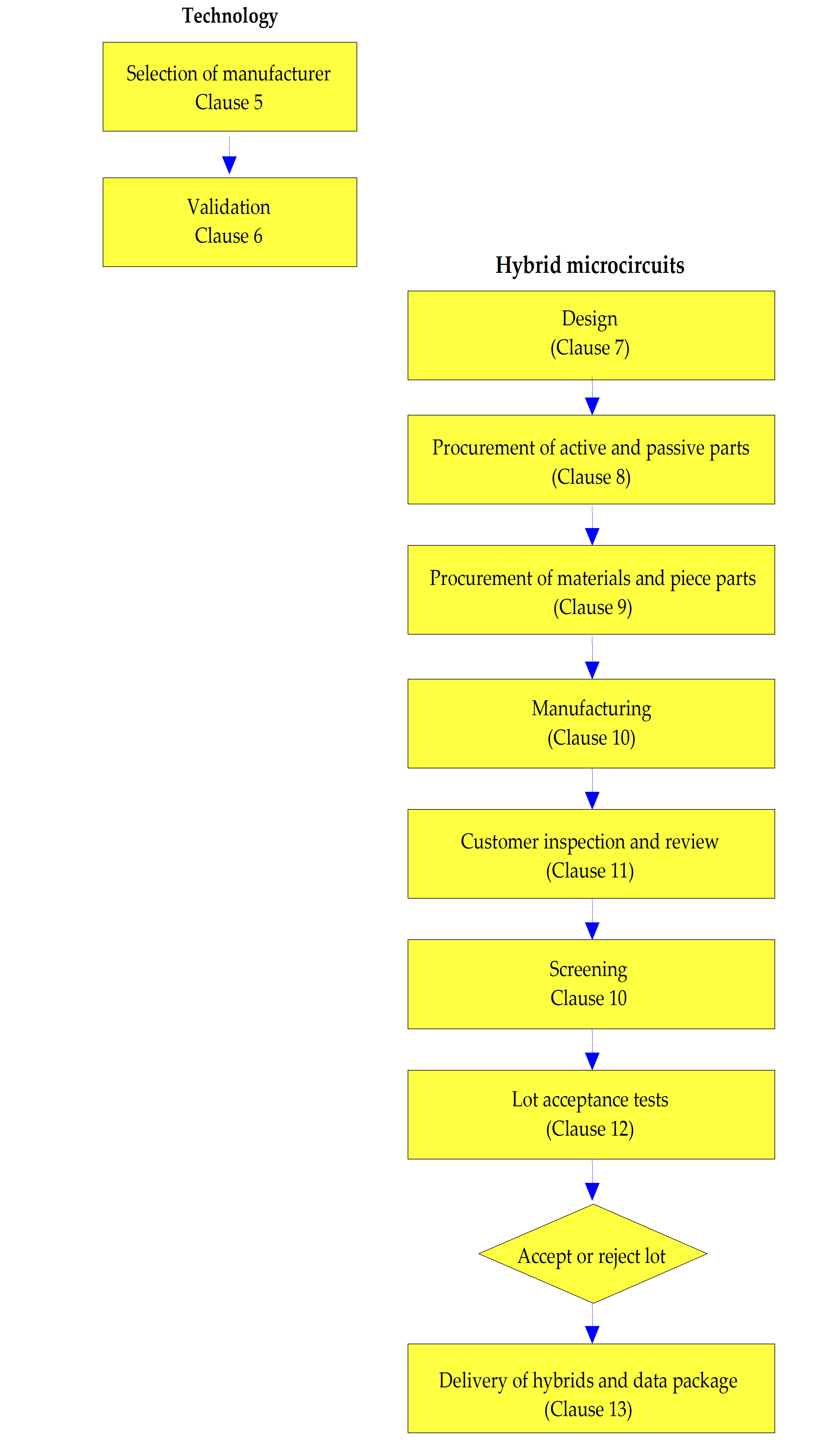 Figure 41: Sequence of activities in the procurement of hybrid microcircuits
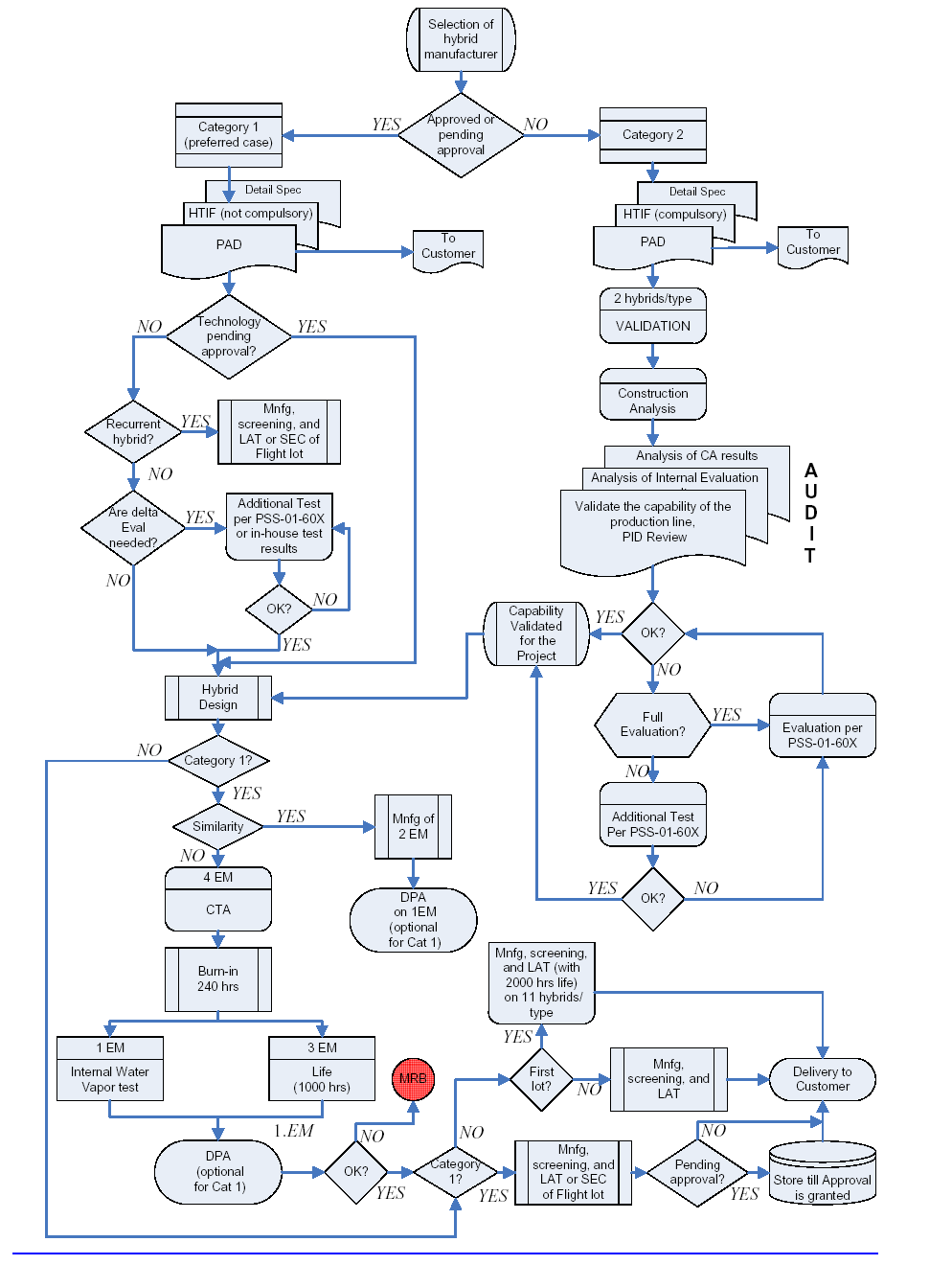 Figure 42: Hybrids procurement flow
Selection of hybrid microcircuit manufacturer
General
All manufacturers that are selected for producing hybrids shall be validated as described in Clause 6.
Hybrid microcircuit manufacturer categories
Category 1 manufacturer (preferred case)
A supplier who wishes to use (or manufacture) hybrid circuits for a space project shall procure (or produce) them from a production line that has been approved or is pending approval by the approving authority.
All hybrid circuits shall be manufactured using the basic processes and materials, and in conformance with the manufacturing and inspection procedures as described in the PID that has been approved by the approving authority.
The PID shall contain as a minimum:
- the manufacturing and inspection flow chart;
- the list of applicable documents with approved revision;
- the general organization of the production line;
- the approved domain: authorized parts, materials, processes and reworks;
- the list of manufacturing, inspection and failure analysis equipment;
- the list of hybrids manufactured in conformance with the approved PID.
Category 2 manufacturer (nonpreferred case)
A supplier wishing to use (or manufacture) hybrid circuits from a production line that has not been approved by the approving authority shall:
- justify its requirements to the customer (especially if this involves developing a new circuit), and
- satisfy the validation conditions described in Clause 6.
Validation procedure for a hybrid microcircuit manufacturer
General
Validation of manufacturers and production lines shall be conducted jointly by the supplier using the hybrid circuit and the customer, and involving upper level customers where relevant.
In the case of confidential information, these activities may be conducted with the support of the approving authority.
Hybrid circuit technology identification form (HTIF)
General
Whatever his status (category 1 or 2) regarding the capability approval, a manufacturer wishing to produce or use hybrid circuits shall complete a hybrid circuit technology identification form (HTIF) for each circuit, in conformance with Annex A.
For category 2 manufacturers, this form shall be included with the part approval document (PAD) as described in 6.2.4.
The format of the PAD is defined in ECSS-Q-ST-60, Annex A.
HTIF for approved manufacturers (category 1)
With justification, it is not mandatory, for a category 1 manufacturer, to deliver the HTIF to the customer.
A category 1 manufacturer shall issue a CoC to the customer to confirm that the proposed hybrid circuit conforms to the domain approved by the approving authority.
As a minimum, the HTIF reference and CoC shall be included in the PAD with reference to the applicable PID.
If the technologies used are not entirely covered by the applicable PID, the manufacturer shall carry out additional (delta-)evaluation tests or prove that he has adequate inhouse test results.
See the relevant PSS evaluation plans in ESA-PSS-01-605, ESA-PSS-01-606, and ESA-PSS-01-612.
This (delta-)evaluation programme shall be referenced in the PAD.
The test results shall be approved by the first level supplier.
The manufacturer shall supply these circuits according to the procurement rules defined for the project as per the requirements in this standard.
HTIF for manufacturer pending capability approval by the approving authority (category 1)
Overview
Manufacturers of hybrid circuits are considered to be pending capability approval by the approving authority when:
they have successfully completed the “evaluation” phase,
their PID has been approved, and
they have begun the “approval” phase (see ESA-PSS-01-605, ESA-PSS-01-606, and ESA-PSS-01-612).
Requirements
Manufacturers shall only use the technologies that have been tested in the evaluation phase and are referenced in the PID.
Manufacturers may manufacture circuits while the approval phase is being carried out in conformance with the PID.
Manufacturers shall not deliver these circuits until capability approval has been formally acquired.
HTIF for manufacturer not approved by the approving authority (category 2)
Overview
For category 2 manufacturers, the review and validation activities for the production lines are described in clause 6.3.
Requirements
The review and validation activities for the production lines for category 2 manufacturers shall be implemented at the PDR milestone of the project.
A category 2 manufacturer shall supply an HTIF in conformance with Annex A and include it as part of the PAD.
In case of confidentiality of particular materials or processes, claimed by category 2 manufacturers, the HTIF attached to the PAD may leave undisclosed the confidentiality elements, provided that these aspects are covered and discussed during the quality and technical audit as described in clause 6.3.3.
The HTIF shall be in conformance with the technological domain validated for the project.
The manufacturer shall produce the hybrid circuits for the project which conform to the same common requirements as for category 1 manufacturers and additional requirements as defined in this Standard.
Validation of category 2 manufacturers
General
Category 2 manufacturers shall be validated in conformance with the requirements in this clause 6.3.
Construction analysis on representative samples
Two circuits per hybrid type shall be supplied by the supplier for construction analysis.
The quality level of these circuits shall be the same as the one specified by the project.
Quality and technical audit
After construction analysis, a quality and technical audit shall be carried out by the supplier as follows:
- Present the results of the construction analysis.
- Analyse the results of internal evaluations of the technologies implemented by the manufacturer. Compare these previously obtained results to the tests defined in the evaluation plans (see ESA-PSS-01-606, ESA-PSS-01-605, and ESA-PSS-01-612), and apply the following criteria.
- If the results of the tests are successful, consider the manufacturer “validated”, but only for the project.
- If only some of the results are successful, perform additional tests pertaining to the failures (see the evaluation plans ESA-PSS-01-606, ESA-PSS-01-605, and ESA-PSS-01-612).
- If all the results are unsuccessful, draw up a completely new evaluation plan (see ESA-PSS-01-606, ESA-PSS-01-605, and ESA-PSS-01-612).
- Judge the validity of manufacturer’s inhouse data in conformance with the following criteria:
- Equivalence of the test structure(s) subjected to the inhouse evaluation tests and the hybrid circuits proposed by the project, this “equivalence” including assessment of the following:
technology of the circuit, circuit function, circuit complexity, power dissipation.Comparison between the inhouse evaluation tests and the reference evaluation plans with respect to the severity of the tests (e.g. level, duration, temperature) and the accept or reject criteria applied.* Validate the capability of the production line to meet the quality requirements of the project and ensure the following: - The components, materials and processes used are governed by specifications written, approved by the manufacturer’s quality control departments and that this documentation is applied at the time of the manufacturer’s inhouse evaluation tests.
- The quality control operations on the production line conform in frequency and severity to the “high reliability” requirements.
- The traceability of the finished product and its component parts is guaranteed by the manufacturer and can be used by the customer.
- All the documentation relating to production and quality assurance specified in the process identification document (PID) is approved by the customer.
- Equivalence of the test structure(s) subjected to the inhouse evaluation tests and the hybrid circuits proposed by the project, this “equivalence” including assessment of the following:
For guidelines for carrying out such audits see ESA-PSS-01-607 and ESA-PSS-01-611.
Design requirements
General
Overview
The “design” of a hybrid circuit includes the initial activities to be undertaken by a manufacturer in order to implement specific electrical functions, derived from a circuit diagram, in a finished hybrid.
Design activities
The design activities of a hybrid circuit shall, as a minimum, include the following:
- Selection of technology.
- Selection of addedon components, i.e. defining the types of chip components used in the hybrid and their manufacturers.
- Definition of the physical layout of the hybrid circuit, i.e. the interconnections in the hybrid to enable the electrical function.
- Application of the derating requirements in conformance with ECSS-Q-ST-30-11.
- Implementation of the thermal management criteria in the case of power circuits.
- Mechanical, dimensional verification.
- Verification of the radiation related requirements for the addedon components and the whole hybrid circuit.
- The activities requested by the customer to ensure that the predicted failure rate of the hybrid circuit is compatible with the reliability target of the equipment concerned (FMECA, reliability calculation and worst case analysis).
When selecting the technology in conformance with 7.1.2a.1, the technology shall be as specified in the PID and described in the hybrid technology identification form (HTIF) specified in Annex A.
When selecting the addedon components in conformance with 7.1.2a.2, the selection shall conform to the requirements specified in the PID.
When defining the physical layout of the hybrid circuit in conformance with 7.1.2a.3, the layout of the hybrid circuit shall conform to the design rules defined in the specification called up by the approved PID.
Detail specification for hybrid circuits
A detail specification for each type of hybrid circuit shall be drawn up in conformance with Annex B.
The maximum rating and drifts of electrical parameters shall be established from the following:
- the detail specification for the chip components,
- the results obtained on prototypes and engineering models.
The manufacturer shall demonstrate the consistency between the maximum ratings and drifts specified for the hybrid circuit and those for each of the chip components.
Any deviations in the burnin and life test temperatures as specified in the detail specification (Annex B) shall be subject to a request for deviation.
Design approval (circuit type approval)
General
Overview
The procedure for design approval of a hybrid circuit depends on the following:
Its “non similarity” to a circuit developed or being developed for the project, or a circuit already developed and approved within the framework of a previous project.
Its “similarity” to a circuit developed or being developed for the project, or a circuit already developed and approved within the framework of a previous project.
The “recurrence” of a circuit which has already been used (developed, approved, manufactured) within the framework of a previous project.
Requirements
Similarity shall be proposed by the manufacturer to the customer by using a similarity form in conformance with Annex C.
Similarity is assessed on the basis of the HTIF and this similarity form.
The similarity form shall be enclosed with the request for use (PAD).
Procedure for a new hybrid circuit which is “non similar” to a reference circuit
The procedure for the design approval for a new circuit which is not similar to an approved circuit shall respect the following:
- Manufacture four hybrids with, as a minimum, an EM quality level.
- Take electrical measurements at ambient temperature in conformance with Tables 2 and 4 of the detail specification provided in Annex B.
Table 3 is optional.
- Subject the four hybrids to burnin over a period of 240 h in conformance with Table 5 of the detail specification provided in Annex B.
- Take electrical measurements in conformance with Tables 4, 2 and 3 of the detail specification provided in Annex B.
- Measure the internal water vapour content of one hybrid in conformance with MIL-STD-883 method 1018, taking as acceptance criterion: 5 000 10-6 parts water vapour maximum at 100 C.
- Perform a DPA on the hybrid submitted to 7.3.2a.5 in conformance with clause 14.
- Analyse the observed defect to determine its cause
For example, basic technology, component quality, design.
* No failure allowed.
* For category 1 manufacturers the DPA is optional.
- Perform a life test shall for a duration of 1 000 h on three hybrids, in conformance with Table 7 of the detail specification provided in Annex B.
- Take electrical measurements in conformance with Tables 2, 3 and 6 of the detail specification provided in Annex B.
- No failure allowed.
- Perform a DPA on one of the three hybrids submitted to life test.
- No failure allowed.
- For category 1 manufacturers the DPA is optional.
CTA can be performed on the first flight model hybrid providing project agreement.
To perform the internal water vapour content measurement in conformance with 7.3.2.a.5, a screening reject may be used.
Procedure for a new hybrid circuit which is “similar” to a reference circuit
The procedure for the design approval of a new hybrid which is similar to an approved circuit shall be as follows:
- Manufacture two hybrids with, as a minimum, an EM quality level.
- Take electrical measurements in conformance with Tables 2 and 3 of the detail specification provided in Annex B.
- No failure allowed.
- Perform a DPA shall be performed on one of the two hybrids,
- No failure allowed.
- For category 1 manufacturers the DPA is optional.
Procedure for a “recurrent” hybrid circuit
A hybrid circuit shall be considered to be “recurrent” when the following conditions apply:
- Its design has already been approved without any deviations (in conformance with the procedures described in clause 7.3.2 or 7.3.3) for a previous project.
- Its FM version has the same references, detail specification, HTIF and list of chip component suppliers (if not included in the HTIF) as the flight hybrid produced within the framework of a previous project, taking into account alerts and deviations.
- Its conditions of use and constraints are similar in nature and severity to those for a previous project.
A “recurrent” hybrid circuit may be manufactured without any further design validation.
If one of the conditions described not be met, the design shall be approved in conformance with clause 7.3.2 or 7.3.3.
The customer may reject the case for a recurrent circuit if the information supplied is considered to be inadequate.
Procurement of passive and active chips
General
Introduction
The procurement of add on parts is detailed below. The flow for chip components is illustrated in Figure 81.
Active and passive chips form a subset of all electronic components.
Active chips are diodes, transistors, and integrated circuits supplied in the form of bare chips.
The most commonly used passive chips include resistors, capacitors and inductors.
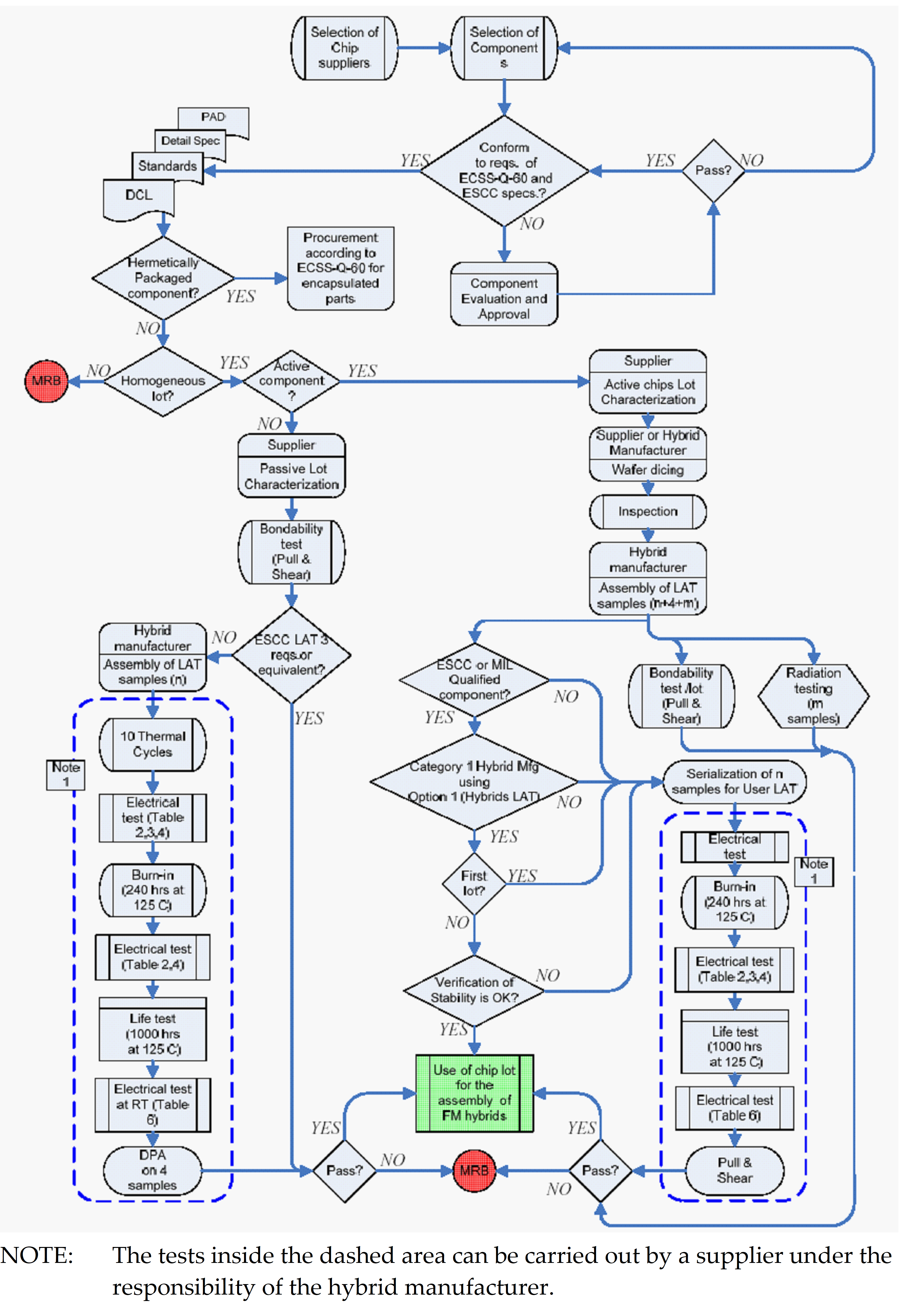 Figure 81: Flow of Procurement of Active and Passive components
Selecting chip suppliers
The manufacturer of the hybrid shall ensure that the selected component manufacturers conform to the component selection requirements of ECSS-Q-ST-60 and the ESCC specifications.
Design and procurement of MMIC dies shall be done in conformance with ECSS-Q-ST-60-12.
The chip component supplier can be either the chip manufacturer or a “chip processor” approved by the hybrid manufacturer.
For chip components which are qualified in an “encapsulated version”, it is the responsibility of the hybrid manufacturer to verify that “qualified chip components” are procured.
If nonqualified components are procured, a component evaluation and approval testing programme shall be implemented in conformance with the component approval requirements of ECSS-Q-ST-60.
It is the responsibility of the hybrid manufacturer to demonstrate that the procured chips are reliable in the hybrid environment, i.e. the materials and processes used are compatible.
Specifications
Existing European components specification systems, i.e. ESCC and CECC or equivalent MIL, should be used.
Whenever a new procurement specification is established, it shall conform to one of the existing European standardization systems.
All components shall be procured in conformance with the specifications in the PID and listed in the DCL, and all specifications shall be subject to configuration control.
The detail specifications for the chip components shall include the electrical parameters that have been verified during the lot characterization tests, the screening conditions, and life tests as well as aspects such as size and chip mask, when applicable.
Requirements for chip lots
All chips shall be procured as traceable homogeneous lots, defined as follows:
- For active chips, a homogenous lot is defined as a unique lot with respect to diffusion, metallization and passivation processes.
- For passive chips, a homogeneous lot is defined as a unique lot with respect to firing or metallization.
Procurement of passive chips
General
Each lot of passive chips shall be characterized by the supplier as follows and checked and accepted by the customer:
- Conformance of the passive chip to its detail specification (e.g. size, terminations).
- Traceability and homogeneity of the lot.
- 100 % electrical measurements at ambient temperature.
- 100 % visual inspection in conformance with ESCC 2043000, ESCC 2053000, ESCC 2093000, ESCC 2044000, ESCC 2054000, ESCC 2094000 or MIL-STD-883 method 2032 or equivalent. For each lot of passive chips, a sample shall undergo a bondability test and a lot acceptance test.
Bondability test
The bondability test shall be performed on four chips per lot, or ten chips per family, assembled by the hybrid manufacturer, using its materials and processes.
If wire bonding is used a minimum of 22 wires shall be tested.
If bimetallic bonding (Au-Al) is used 8.3.2.c applies
A shear test shall then be performed on all the chips.
Results shall conform to MIL-STD-883 method 2011 for bond pull strength and MIL-STD-883 method 2019 for die shear strength, with no failure allowed.
acceptance test (LAT)
acceptance test (LAT) requirements shall be selected depending on the origin of the passive chips, as follows:
- For ESCC or MILequivalent qualified, screened and burnedin passive chips, only ESCC LAT 3 requirements or equivalent are applicable.
- For all other cases, ensure that a sample batch of “n” chips is assembled by the hybrid manufacturer with its materials and processes, and the following sequence of tests is performed either by the manufacturer, or by a subcontractor under the responsibility of the manufacturer:
- Perform thermal cycling (10 cycles) in conformance with MIL-STD-883 method 1010 condition B, if this was not already performed during the screening tests.
- Take electrical measurements before burnin in conformance with Tables 2, 3 and 4 of the passive chip detail specification provided in Annex B and ensure that the maximum number of rejects is as given in Table 81.
- Subject the samples to burnin over a period of 240 h at 125 C.
- Take electrical measurements at ambient temperature and the drift values calculated in conformance with Tables 2 and 4 of the passive chip detail specification, and ensure that the maximum number of rejects is as given in Table 81.
- Perform a lifetest for a period of 1 000 h at 125 C.
- Take electrical measurements at 25 C in conformance with Table 6 of the passive chip detail specification, and ensure that no failure occurs.
- Perform a DPA on four samples after the lifetest as defined below, and ensure that no failure occurs:
a visual inspection in conformance with MIL-STD-883 method 2032; a wire pull test in conformance with MIL-STD-883 method 2011;a shear test on chips in conformance with MIL-STD-883 method 2019 or in conformance with the PID.The LAT acceptance criteria shall be as given in Table 81.
Table 81: Sample size and acceptance criteria for LAT of passive chips
|
“n” samples
|
Number of defects allowed after:
|
Number of accumulated defects for:
| |||
|
Electrical test
|
Burnin
|
Life test
|
Rejection
|
Acceptance
| |
|
18
|
1
|
1
|
0
|
2
|
1
|
|
11
|
0
|
0
|
0
|
1
|
0
|
Procurement of active chips
General
Each lot of active chips shall be characterized by the supplier as follows and checked and accepted by the customer:
- Conformance of the active chip to its detail specification (e.g. size, masks).
- Traceability and homogeneity of the lot.
- 100 % probe testing of the wafers at 25 C and marking of chips that do not conform.
- Visual inspection of the wafer in conformance with:
- MIL-STD-883 method 2010 condition A or B (integrated circuits);
- MIL-STD-750 methods 2072 and 2073 (diodes and transistors).
- SEM inspection in conformance with the component technology (i.e. in case of metallization over oxide steps). Once the wafer has been scribed and diced, a 100 % visual inspection shall be carried out on the chip supplier’s premises or as part of the hybrid manufacturer’s incoming inspection in conformance with the following:
- MIL-STD-883 method 2010 condition A (integrated circuits), ESCC 2045010 (microwave devices), ESCC 2049010 (monolithic microwave devices).
- MIL-STD-750 methods 2072 and 2073 (diodes and transistors).
When radiation lot acceptance is considered necessary for a part in packaged form (lot by lot variability components), the same policy shall be applied for the part in die form.
For each lot of active chips, a sample shall undergo a bondability test and customer lot acceptance test (user LAT).
Bondability test
The bondability test shall be performed on four chips assembled by the hybrid manufacturer with its materials and processes.
A bond pull strength test shall be performed on 22 wires (or all the wires if less) and a shear test on the four chips.
For bimetallic bonding (goldaluminium) ageing (1 h at 300 C or the equivalent timetemperature combination with a 0,92 eV activation energy basis) shall be performed before the pull test.
Results shall conform respectively to MIL-STD-883 method 2011 for bond pull strength and MIL-STD-883 method 2019 for die shear strength, with no failure allowed.
User LAT
Overview
User LAT is the performance of burnin or life test and electrical measurements in order to verify the electrical characteristics of the chip lot when the chip is assembled with the hybrid manufacturer processes and package environment (which can be different from the chip manufacturer processes).
User LAT requirements
Qualified (ESCC or MIL) parts (family or type in packaged or nonpackaged form)
User LAT shall be performed for the first lot procured in conformance with Table 82.
For the subsequent lot, and in the case of good results on the first lot, the hybrid manufacturer shall verify the stability of the frontend manufacturing.
If this verification is satisfactory, a user LAT may be deleted providing that the option 1 lot acceptance testing is performed at a hybrid level.
Nonqualified parts:
User LAT shall be performed on each lot in conformance with Table 82.
MMIC dies
User LAT shall be performed either on actual MMICs or on TCVs (technological characterization vehicles present on the same wafer of the MMICs) providing that these TCV dies are designed in conformance with the design manual of the MMIC foundry.
General
User LAT shall be performed, for each type of active chip and for each lot, on a batch of “n” assembled and encapsulated samples.
The values for “n” and the acceptance criteria are given in Table 82.
Table 82: Sample size and acceptance criteria for user LAT on active chips
|
“n” samples
|
Number of failures allowed for:
|
Number of accumulated failures for:
| |||
|
Electrical test a
|
Burnin
|
Life test
|
Rejection
|
Acceptance
| |
|
38
|
3
|
2
|
0
|
4
|
3
|
|
25
|
2
|
1
|
0
|
3
|
2
|
|
18
|
1
|
1
|
0
|
2
|
1
|
|
11
|
0
|
0
|
0
|
1
|
0
|
|
a Defects due to the assembly process are not be considered to be a failure.
| |||||
After encapsulation, the sample batch of “n” chips shall be subjected, either by the hybrid manufacturer or by a subcontractor under his/her responsibility, to the following procedure:
- Serialization.
- Take electrical measurements at ambient temperatures in conformance with Table 2 of the chip detail specification.
Table 3 optional.
- Take electrical measurements before burnin in conformance with Table 4 of the chip detail specification, values shall be recorded.
- Subject the samples to burnin over a period of 240 h at 125 C in conformance with the chip detail specification.
- Take electrical measurements at ambient and extreme temperatures in conformance with Tables 2 and 3 and the drift calculated in conformance with Table 4 of the chip detail specification, with the maximum number of rejects allowed given in Table 82.
- Perform a lifetest for a period of 1 000 hours at 125 C in conformance with the chip detail specification.
- Take electrical measurements in conformance with Table 6 of the chip detail specification with the maximum number of rejects allowed given in Table 82.
- Perform a wire pull test in conformance with MIL-STD-883 method 2011 on 22 wires or on all the wires if less, with no failure allowed.
- Perform a shear test on the assembled chips in conformance with MIL-STD-883 method 2019 on 4 chips, with no failure allowed.
Procurement of hermetically encapsulated chips
Hermetically encapsulated chips shall be fully characterized, screened and tested before being mounted on the film network.
The hermetically encapsulated components to be used on hybrids shall be procured in conformance with component selection requirements of ECSS-Q-ST-60, or fully tested and screened in conformance with a procedure that is agreed upon by the approving authority during capability approval, and specified in the PID.
Assembly tests of the packaged component shall be performed as specified in the PID.
Procurement of materials and piece parts
Overview
Materials and piece parts include:
Package, lid and cover,
Interconnection substrate,
Attachment medium,
Wires and ribbons,
Carriers and mechanical parts.
Selection of materials and piece parts
The hybrid manufacturer shall ensure that the selected materials and piece parts conform to the “Material control” requirements in ECSS-Q-ST-70.
Pure Tin (≥ 97 %) shall not be used on internal and external elements of the hybrid, this includes underplating.
The hybrid manufacturer shall demonstrate that the procured materials and piece parts have no impact on the reliability of the passive and active parts in the hybrid environment.
Specifications
All materials and piece parts shall be procured in conformance with the specifications in the PID.
All specifications shall be subjected to configuration control.
The procurement specification of materials and piece parts shall include, as a minimum, the following:
- The physical and chemical characteristics guaranteed by the supplier with reference to the test methods.
- The outgoing tests performed on each lot by the supplier with reference to the test methods and acceptance criteria.
- The provisions for lot definition and traceability.
- The delivery conditions. Whenever a new procurement specification is established, it shall conform to a European standardization system.
Requirements for materials and piece parts
All materials and piece parts shall be procured as traceable homogeneous lots.
The definition of the materials and piece parts shall be specified in the procurement specification.
Each material and piece part shall be submitted to an incoming inspection procedure, which defines the inspections and tests to be carried out to verify the characteristics guaranteed by the supplier (confidence test) and to verify the compatibility of the item with the hybrid application (user tests).
Manufacturing and screening of hybrid circuit lots
Manufacturing
All manufacturing and inspection operations shall be conducted in conformance with the corresponding manufacturer PID.
Marking
General
Marking shall be on the body of the hybrid circuit.
Apart from serialization, all marking shall be clearly visible when normal mounting procedures are followed.
If a hybrid is too small to accommodate all marking, the device shall show, as a minimum, the polarity or lead identification and as much marking as is possible in the prescribed order of precedence as defined in 10.2.1f below.
Any marking that cannot be accommodated on the cases themselves shall be shown on the individual containers, excluding the serial numbers, which shall be shown on a tag attached to one of the leads.
Marking shall remain legible after all the tests specified in this Standard have been performed and shall withstand all solvents used in conformance with MIL-STD-883 method 2015.
Each hybrid circuit shall be marked with the following information in the given order of precedence:
- Polarity or lead identification as defined in its detail specification specified in Annex B.
- Part number as defined in its detail specification specified in Annex B, followed by the suffix 1 or 2, depending on the testing level.
- Manufacturing date code, a 4 digit code used where: the first two digits are the last two digits of the calendar year: the last two digits are the number of the week in which the hybrid was encapsulated
- For testing level 1, the serial number, consisting of a sequential number of two or more digits for each selected sublot.
- Manufacturer’s name, symbol or trade mark.
The production lot number may be also marked.
The serial number specified in 10.2.1f.4 shall not be duplicated when more than one selected sublot has been taken from a production lot.
Special cases
If a hybrid microcircuit contains Beryllium oxide substrates or carriers, it shall be marked with the notation: « Contains BeO », or in the case of insufficient space on the package, indicate only « BeO ».
If a hybrid microcircuit is sensitive to electrostatic discharge, the ESD sensitivity classification shall be marked on the package.
Screening
General
The screening test sequence for FM hybrid circuits shall, as a minimum, conform to the requirements of Figure 101.
Two nominal levels (level 1 or level 2) shall be chosen depending on the project’s mission characteristics
For example, quality level, or inorbit lifetime.
The sequence of all tests to be performed shall be as given in Figure 101 unless the manufacturer has formally requested and obtained permission from the customer to deviate from this sequence.
All hybrids for delivery and all hybrids used for environmental and endurance tests shall meet all of the relevant screening test sequence requirements.
Any hybrid that does not meet these requirements shall be removed from the lot.
|
Final production step except encapsulation
| ||||||
|
Test no.
|
Inspection and screening test
|
Specification and test method
|
Test condition
|
Sample size
|
Testing level 1
|
Testing level 2
|
|
1
|
Thermographic
|
See 10.3.2
|
|
1 piece
|
R
|
|
|
2
|
Nondestructive bond pull
|
MIL-STD-883 Method 2023
|
|
100 %
|
O
|
|
|
3
|
Preseal burnin
|
See 10.3.3
|
See detail specification
|
100 %
|
O
|
O
|
|
4
|
Electrical test
|
In conformance with manufacturing specification
|
|
100 %
|
O
|
O
|
|
5
|
Photograph of circuit
|
See 10.3.4
|
|
1 piece
|
O
|
|
|
6
|
Precap visual inspection
|
MIL-STD-883 Method 2017 Class K
|
|
100 %
|
R
|
R
|
|
Key: R = Required O = Optional
| ||||||
|
Vacuum bakeout: in conformance with PID
| ||||||
|

|
||||||
Figure 101: Screening test sequence
|
Encapsulation / in conformance with PID
| ||||||
|
Test no.
|
Inspection and screening test
|
Specification and test method
|
Test condition
|
Sample size
|
Testing level 1
|
Testing level 2
|
|
7
|
Stabilization bake
|
MIL-STD-883 Method 1008
|
Condition B 72 hours
|
100 %
|
O
|
O
|
|
8
|
Thermal cycling
|
MIL-STD-883 Method 1010
|
Condition B 10 cycles
|
100 %
|
R
|
R
|
|
9
|
Mechanical shock or constant acceleration
|
MIL-STD-883 Method 2002 or 2001
|
Y1 axis only (see 10.3.5)
|
100 %
|
R
|
R
|
|
10
|
Particle impact noise detection (PIND)
|
MIL-STD-883 Method 2020 specification
|
Condition A
|
100 %
|
R
|
R
|
|
11
|
Fine leak
|
MIL-STD-883 Method 1014
|
Condition A2 (see 10.3.7)
|
100 %
|
O
|
O
|
|
12
|
Gross leak
|
MIL-STD-883 Method 1014
|
Condition C1 or C2 (see 10.3.7)
|
100 %
|
O
|
O
|
|
13
|
Physical dimensions
|
MIL-STD-883 Method 2016
|
See 10.3.8
|
3 hybrids
|
R
|
R
|
|
Key: R = Required O = Optional
| ||||||
|
Marking and serialization
| ||||||
|

|
||||||
Figure 101: Screening test sequence (Part 2)
|
Test No.
|
Inspection and screening test
|
Specification and test method
|
Test condition
|
Sample size
|
Testing level 1
|
Testing level 2
|
|
14
|
Pre burnin electrical measurements
|
Detail specification Table 4 and Table 2
|
Ambient temperature
|
100 %
|
R
|
R
|
|
15
|
Burnin
|
Detail specification
|
Detail specification Table 5
|
100 %
|
R
|
R
|
|
16
|
Parameter drift calculation
|
Detail specification Table 4
|
|
100 %
|
R
|
|
|
17
|
Electrical measurements ambient temperature
|
Detail specification Table 2
|
|
100 %
|
R
|
R
|
|
18
|
Electrical measurements high and low temperature
|
Detail specification Table 3
|
|
100 %
|
R
|
R
|
|
19
|
Radiographic inspection
|
MIL-STD-883 Method 2012
|
See 10.3.10
|
100 %
|
R
|
R
|
|
20
|
Fine leak
|
MIL-STD-883 Method 1014
|
Condition A2
|
100 %
|
R
|
R
|
|
21
|
Gross leak
|
MIL-STD-883 Method 1014
|
Condition C1 or C2
|
100 %
|
R
|
R
|
|
22
|
External visual inspection
|
MIL-STD-883 Method 2009.8
|
|
100 %
|
R
|
R
|
|
Key: R = Required O = Optional
| ||||||
Figure 101: Screening test sequence (Part 3)
Thermographic test
Thermographic test shall be performed only to hybrid circuits where thermal studies or design approval tests during CTA activities have indicated the existence of hot spots at maximum rated power.
A point at which the delta temperature between the surface and the case is higher than 30 C for active components, or higher than 60 C for passive components, shall be considered as a hot spot.
by lot, a suitable evaluation method shall be used to evaluate the temperature reached by the critical components when powered and thus demonstrate thermal resistance reproducibility throughout the assembly process.
If an infrared microscope is used, the circuit shall be coated to obtain a uniform emissivity factor from the metallization surfaces.
This test is destructive.
Preseal burnin
Preseal burnin need not be performed.
Pre-seal burn-in is optional.
If Pre-seal burn-in test is performed, the test procedure, the environment and duration shall be approved as part of the line capability approval activity by the approving authority.
Preseal burnin shall be performed in an inert atmosphere.
The total burnin time shall not be less than 240 h.
The total burn-in time may be divided between preseal burnin and postseal burnin, provided that the latter lasts 144 h or more.
Photograph of circuits
If a photograph is not made as part of the screening, it shall be done during the CTA or during the manufacturing of the first production lot.
Magnification shall be such that the layout can be easily identified.
The same circuit shall also be photographed at a magnification at which the chip surface pattern is easily identifiable.
Conditions for constant acceleration and mechanical shock
The test conditions for constant acceleration and mechanical shock shall be a function of the hybrid package size, as specified in Table 101.
Table 101: Test conditions for constant acceleration and mechanical shock
|
Hybrid package size
|
Constant acceleration
|
Mechanical shock
|
|
Up to 25,4 mm 25,4 mm
|
10 000 g(Condition B)
|
1 500 g – 0,5 ms(Condition B)
|
|
From 25,4 mm 25,4 mmUp to 25,4 mm 50,8 mm
|
5 000 g(Condition A)
|
1 500 g – 0,5 ms(Condition B)
|
|
Above 25,4 mm 50,8 mm
|
Not applicable
|
1 000 g – 0,5 ms
|
|
NOTE: These conditions can be modified on a case by case basis through a duly justified RFD (request for deviation).
| ||
Test condition for PIND
This test may be waived by the approving authority in the case of internally coated hybrids.
Leak tests
Pressurization and time shall depend on the package sizes in conformance with MIL-STD-883 Method 1014.
The exact test condition shall be as specified in the PID.
The applicable package test condition shall be as specified in the Detail Specification.
This test can be performed, at this point in the sequence, at the manufacturer’s discretion.
Physical dimensions
Physical dimension measurements may be omitted where the hybrid manufacturer is also the customer.
Burnin test
Taking into account the power applied, the oven temperature shall be defined so that the junction temperature of the most stressed active chip component shall be between 125 C and 150 C.
If another temperature is selected, the burnin duration shall be adjusted in conformance with MIL-STD-883 method 1015.
Radiographic inspection
This inspection may be performed at any point during the test sequence.
The performance of this test depends on the technology.
This test may be omitted only in the case of aluminium wires and epoxy bonding of chips.
rejection
Definition of failure modes
General
A hybrid shall be considered as having failed if it exhibits one or more of the failure modes described in clauses 10.4.1.2 to 10.4.1.5.
Parameter drift failure
When the changes between the 0 hour and the 240 hour measurements of burnin, based on the 0 hour reading, are larger than the specified delta limit shall be considered a parameter drift failure.
The acceptable delta limit is specified in Table 4 of the hybrid detail specification specified in Annex B.
Parameter limit failure
When one or more parameters exceed the limits shown in Table 2 or Table 3 of the hybrid detail specification (specified in Annex B) shall be considered a parameter limit failure.
Any hybrid, that exhibits a limit failure before burnin shall be rejected, but shall not be counted when determining the lot rejection.
PIND failure
A hybrid which when tested in conformance with the provisions of MIL-STD-883, Method 2020 Condition A, produces noise bursts as detected by any of the three detection systems shall be considered as a PIND failure.
Background noise may be excluded, except those caused by the shock blows, during the monitoring periods.
Other Failures
A hybrid shall be considered to be a failure if any of the following occur:
- catastrophic failure,
- mechanical failure,
- handling failure,
- lost component.
Criteria for lot rejection
For parameter drift failure, if the number of failed hybrids exceeds 5 % PDA of the number of hybrids submitted to the burnin and electrical measurements, the lot shall be rejected.
If the cumulative total of parameter drift failures (see clause 10.4.1.2) and parameter limit failures (see clause 10.4.1.3) exceeds 10 % PDA of the number of hybrids submitted to the burnin and electrical measurements, the lot shall be rejected.
For PIND testing, the hybrids the following shall be perform:
- Submit to testing a maximum of 5 times.
- After each run, remove defective hybrids from the lot.
- Accept the lot on any of the 5 runs if the percentage of defective devices is less than 1 % of the devices tested (or 1, whichever is greater).
- Reject the lots that do not meet the 1 % PDA on the 5th run or which at any time exceed 25 % cumulative failures.
Disposition of rejected lots
Rejected lots shall be segregated and kept in bonded store for further investigation at the customer’s discretion.
Repair provisions
General
All repair processes carried out on hybrid circuits shall be approved and performed in conformance with the procedures specified in the approved PID.
Element replacement
Any polymer attached element may be replaced twice at a given location on any hybrid circuit.
Any metallic attached element may be replaced once at a given location.
The total number of replacements shall be limited to a maximum of 10 % of the total number of elements in the hybrid circuit.
Except for substrates attached to a package using mechanical fasteners for which the replacement number is not limited, adhesive bonded substrates may be removed, replaced or put into a new package once.
There shall be a maximum of 4 heating cycles for element removal.
It shall be demonstrated that the reliability of the remaining elements is not impacted.
Wire rebonding
Rebonding may be performed for chip to substrate, substrate to package pins, and substrate pad to substrate pad wires.
All rebonds shall be placed on at least 50 % undisturbed metal (excluding probe marks that do not expose underlying metallization or oxide).
If the first bond is not successful, no more than one rebond attempt shall be made at the same place.
Rebonds shall not touch any area of exposed oxide caused by lifted or blistered metal.
The total number of chip to substrate or substrate pad to substrate pad wire rebondings shall be limited to a maximum of 10 % of the total number of wires on the hybrid circuit.
The total number of substrate to package pin wire rebondings shall be limited to a maximum of 15 % of the total number of wires in the hybrid circuit.
Compound bonding
Compound bonding shall not be performed for other than gold.
Compound bonds shall be limited to one bond over the original bond, wire, or ribbon.
When a compound bond is used to secure an existing bond, then the bond shall be nondestructively pull tested.
Only monometallic compound bonds of the same size wire or ribbon shall be used (i.e. the original bond wire and that used for compound bonding shall be of the same material).
Delidding of hybrid circuits
If hybrid circuits may be delidded and relidded for repair:
- The customer is informed before the operation.
- No more than one delidrelid cycle is performed.
When hybrid circuits may be delidded and relidded for repair, suitable screening tests shall be performed on the deliddedrelidded hybrid circuits.
These screening tests shall be defined at the stage when the deliddingrelidding takes place and depend on the type of repair performed.
Customer inspection and review
The degree of customer involvement in the approval of documents and inspections shall be agreed between the customer and the manufacturer at the time of contract negotiation.
The customer shall approve the following documents prepared by the manufacturer:
- the detail specification for the actual hybrid circuit type;
- the PAD;
- the technology identification form (for category 2 only);
- any nonconformance documents. The customer shall be invited to the following key inspections:
- precap visual inspection;
- final acceptance of the hybrids after the performance of all tests including LAT. The customer may delegate another authority to carry out the actual inspections in agreement with the manufacturer.
acceptance tests for hybrid circuits
General
Overview
Quality acceptance of the production of the FM hybrid circuits depends on the category of the manufacturer (category 1 or 2) as defined in clause 5.
Samples
acceptance testing shall be carried out on samples of circuits having passed a complete screening sequence.
acceptance test shall be performed on one of the following:
Option 1: production lot control.
Option 2: production lines under TRB management with periodic testing and statistical process control.
A technology review board (TRB) is a formal group, at manufacturer level, where the design, materials and parts procurement, manufacturing, testing, reliability, and quality assurance functions are represented. The mission of this group is to:
- define and implement a quality management plan for continuous quality improvement;
- identify and analyse the new needs, improvement of the process and nonconformances;
- define and implement the associated validation, preventive and corrective actions;
- inform and justify the evolutions and actions taken on the hybrid production line to the approving authority.
The option chosen by the manufacturer shall be declared in the PID.
Category 1 manufacturer
Option 1: Production lot control
Sampling
For each production lot of hybrid circuits, the number of samples depends on the lot size as given in Table 121.
For a given type of hybrid, there shall be n samples for the first production lot and n-1 samples for the subsequent production lots of the same hybrid type.
Table 121: Sample size for hybrids lot acceptance tests
|
size
|
Sample size for the 1st production lot (n)
|
Sample size for the subsequent production lot(s) (m)
|
|
1 - 25
|
2
|
1
|
|
26 - 50
|
3
|
2
|
|
51 - 90
|
4
|
3
|
|
> 90
|
5
|
4
|
acceptance tests
The LAT samples shall be submitted to the test sequence given in Table 122.
Table 122: Lot acceptance tests and sample size
|
Test sequence
|
Number of samples
|
Test conditions
| |
|
1st lot
|
Subsequent lots
| ||
|
Internal water vapour content
|
1
|
0
|
Before delidding of reference DPA sample in conformance with MIL-STD-883 Method 1018.
|
|
Reference DPA after screening sequence
|
1
|
0
|
In conformance with DPA sequence defined in clause 14.
|
|
Accelerated life test
|
n-1
|
m
|
1 000 h life test at 125 C in conformance with Table 7 of the detail specification (Annex B) (or equivalent timetemperature in conformance with MIL-STD-883 Method 1005).
|
|
Electrical measurements
|
n-1
|
m
|
In conformance with Table 2 and Table 6 of the detail specification (Annex B).
|
|
DPA after life test
|
1
|
1
|
In conformance with DPA sequence defined in clause 14.
|
Acceptance criteria
The production lot shall be accepted if all the following conditions are fulfilled:
- The PDA of each production lot is below the limit as per 10.4.2.
- No failure on the internal water vapour content test.
- No failure on the reference DPA (in the case of the first production lot).
- No failure on the electrical measurements after the lifetest.
- No failure on the DPA sample submitted to life test.
Manufacturer pending approval by the approving authority
For a manufacturer pending capability approval, the lot(s) produced and approved in conformance with the procedure described above shall not be delivered to the project until the approving authority has approved the production line.
Option 2: Lines under TRB management and statistical process control
General
Category 1 manufacturers using this option shall implement a TRB management and statistical process control system that is approved by the approving authority.
Also, Category 1 manufacturers using this option shall establish a statistical process control on the main processes of the manufacturing line.
The Ppk of a process is the longterm capability of the process which reflects the process centering and variability with respect to specification requirements, being the Ppk defined as follows:
![]() where
where
Ts is the upper limit of the specification;
m is the mean value;
Ti is the lower limit of the specification;
is the standard deviation.
See also references [1] and [2].
The Ppk value shall be higher than 1,33 to demonstrate capability of each process.
The higher the Ppk number, the more capable the process.
Under these conditions, and after approval by the approving authority, a lot acceptance test of the hybrids may be applied to the hybrid technological family through a standard evaluation circuit (SEC) with the conditions given in clause 12.2.2.2 to 12.2.2.4.
See Annex D for technological family definition and examples.
Sampling a standard evaluation circuit (SEC)
For each set of production lots grouped in one representative production lot, 1 % of all hybrid circuits concerned shall be sampled with a minimum of one sample manufactured within a maximum period of 3 months.
Production lot acceptance tests
The SEC samples shall be submitted to the test sequence given in Table 123.
Acceptance criteria
The representative production lot shall not be accepted unless all the following conditions are fulfilled:
- The PDA on each representative production lot is below the limit as per 10.4.2.
- The SPC performed during the manufacturing of the representative production lot are under the fixed limits.
- There is no failure in the bond pull test and shear test.
- There is no failure in the seal test and PIND test after ageing.
Category 2 manufacturer (validated for the project)
The sequence of lot acceptance tests for the first production lot shall be as in Figure 121.
For subsequent lots and on condition that the test results for the initial lots are satisfactory, the lot acceptance procedure (category 1 manufacturer, option 1) in conformance with clause 12.2.1 shall be applied for each type.
The specifications and conditions for the tests specified in Figure 121 shall be as given in Table 124.
Table 123: Production acceptance tests and sampling
|
Test sequence
|
SEC number of samples
|
Test conditions
|
|
Seal test
|
1 %
|
MIL-STD-883/1014 A2
|
|
PIND test
|
1 %
|
MIL-STD-883 / 2020 A
|
|
Thermal cycling
|
1 %
|
MIL-STD-883 / 1010
|
|
External visual inspection
|
1 %
|
MIL-STD-883 / 2009.8
|
|
Seal test
|
1 %
|
MIL-STD-883 / 1014 A2
|
|
PIND test
|
1 %
|
MIL-STD-883/ 2020 A
|
|
Internal visual inspection
|
1 %
|
MIL-STD-883 / 2017 S
|
|
Bond pull test
|
1 % (50 % wires)
|
MIL-STD-883 / 2011
|
|
Die shear test
|
1 % (50 % chips)
|
MIL-STD-883 / 2019
|
|
High temperature storage
|
1 %
|
(1h at 300 C or equivalent timetemperature as defined in 8.3.2)
|
|
Bond pull test
|
1 % (remaining wires)
|
MIL-STD-883 / 2011
|
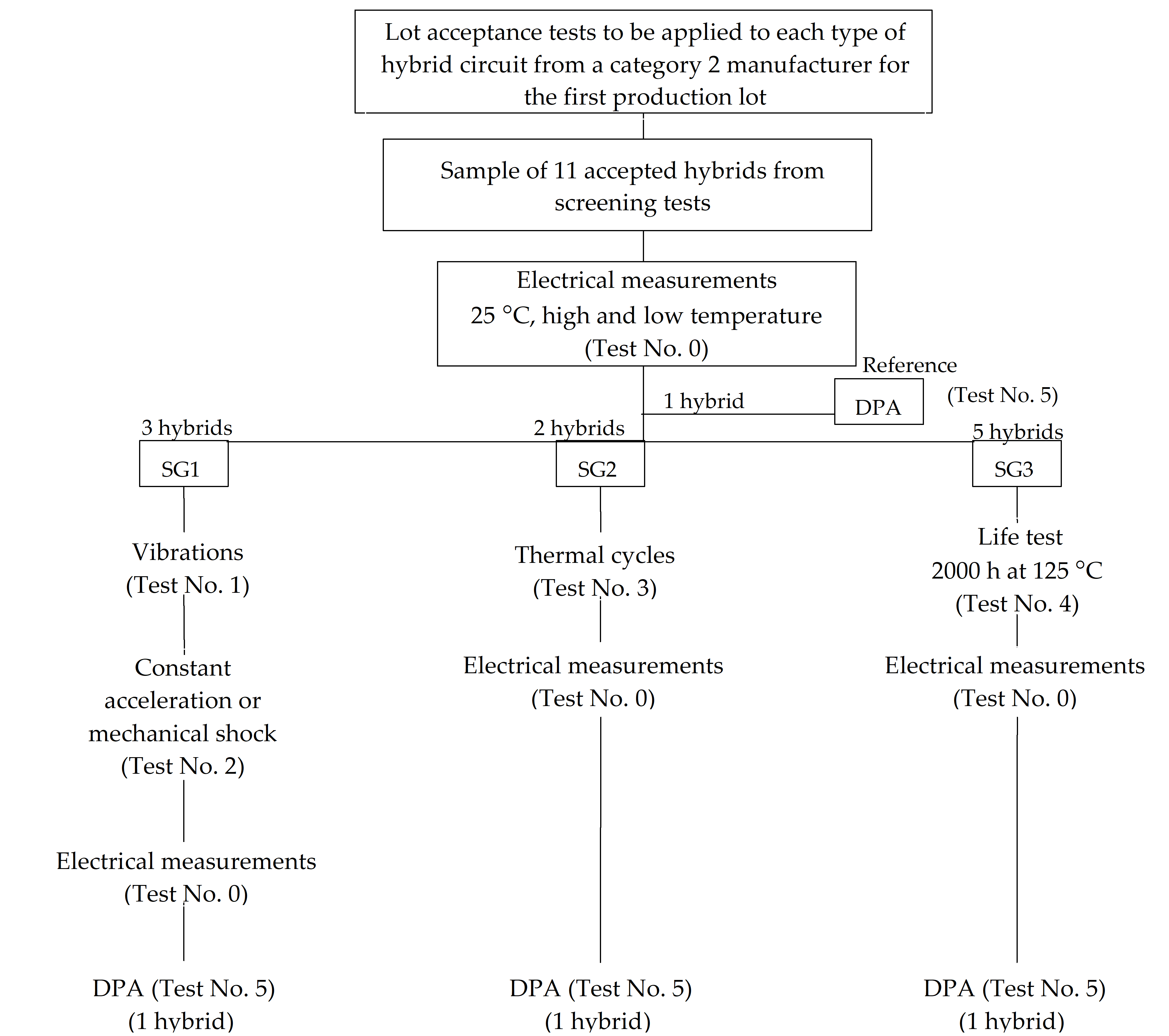 Figure 121: acceptance tests for the first production lot manufactured by a category 2 manufacturer
Table 124: Definition of tests
|
Test No.
|
Test designation
|
Applicable specification MIL-STD-883
|
Comments
|
|
0
|
Electrical measurements at 3 temperatures (ambient, high and low)
|
|
In conformance with detail specification
|
|
1
|
Vibrations
|
Method 2007 condition A
|
Along X and Y axis
|
|
2
|
Constant acceleration or mechanical shocks
|
Method 2001 condition A or B or Method 2002 condition B(see 10.3.5)
|
Along Y1 axisAlong Y1 axis (substrate attach strength)
|
|
3
|
Thermal cycling
|
Method 1010 condition B
|
100 cycles
|
|
4
|
Life test
|
Method 1005
|
Project LAT extended to 2 000 h at 125 C
|
|
5
|
DPA shall be conducted on 1 reference piece and 3 pieces (SG1, SG2, and SG3) in conformance with clause 14.
|
|
|
|
- marking permanency;
|
Method 2015
| ||
|
- lead integrity;
|
Method 2004 condition B2
| ||
|
- solderability;
|
Method 2003
| ||
|
- internal water vapour content.
|
Method 1018 procedure 1
|
Hybrid delivery and data package
General
The delivery of hybrid items shall be agreed with the customer at the contract negotiation stage.
Delivery shall include the following items:
- the delivery lot;
- documentation conforming to the requirements of clause 13.2.
Data documentation
General
Each delivery of a hybrid shall include a data documentation package.
If one is not delivered, all data shall be retained by the manufacturer for a minimum of 5 years, and available during this time to the customer for review upon request.
Depending on the testing level and lot acceptance testing specified, this package shall be agreed with the customer and constitute the following:
- Cover Sheet (or sheets).
- Certificate of conformity (COC).
- MIP reports.
- RFWs, RFDs, NCRs.
- CTA test data (if applicable).
- Burnin and electrical measurement data with delta values.
- acceptance test data including DPA reports (when applicable).
- PDA calculation.
- Photographs and Xray pictures on request.
Cover sheets
The cover sheet(s) of the data documentation package shall include as a minimum:
- Manufacturer’s name and location of manufacturing plant.
- Date and manufacturer’s signature.
- Hybrid circuit type identification.
- Reference to the generic and detail specification, including issue and date.
- Reference to the manufacturing dossier.
- identification.
- Reference to the purchase order.
Certificate of conformity
The certificate of conformity shall include as a minimum:
- Manufacturer’s name and location of manufacturing plant.
- Date and manufacturer’s QA signature.
- Serial numbers of hybrids delivered.
- Reference to the applicable PID including issue and date.
- Reference to the detail specification, including issue and date.
Packaging and despatch
Hybrids shall be packaged and despatched in conformance with the requirements of ESCC 20600.
DPA test sequence
DPA test sequence depends on the technology and shall be performed in conformance with the following methods:
- External visual inspection, MIL-STD-883 Method 2009.8.
- X-rays (if soldered items or gold wires are present), MIL-STD-883 Method 2012.
- SAM inspection, MIL-STD-883 Method 2030.
- Seal test, MIL-STD-883 Method 1014 Condition A2 – Condition C.
- PIND test, MIL-STD-883 Method 2020 Condition A.
- Internal visual inspection, MIL-STD-883 Method 2017 Class K, MIL-STD-883 Method 2010 Condition A, MIL-STD-750 Method 2072, MIL-STD-750 Method 2073, MIL-STD-883 Method 2032.
- SEM inspection, MIL-STD-883 Method 2018 (Provide photos of typical assemblies and possible anomalies).
- Bond pull test, MIL-STD-883 Method 2011 Condition D (Pull all wires).
- Die shear test, MIL-STD-883 Method 2019 (Shear all chips).
ANNEX(normative) Hybrid circuit technology identification form (HTIF) - DRD
DRD identification
Requirement identification and source document
This DRD is called from ECSS-Q-ST-60-05, requirements 6.2.1a and 6.2.4.2b.
Purpose and objective
The hybrid circuit technology identification form (HTIF) is used by a manufacturer (whatever his status, category 1 or 2, regarding the capability approval) wishing to produce or to use a hybrid circuit in a space project, to provide the customer with the appropriate information to assess the technology.
Category 1 manufacturers need not to deliver formally the HTIF to the customer.
Expected response
Scope and content
General
The HTIF shall be as shown in Table A-1.
Table: Hybrid circuit technology identification form (HTIF)
|
Project:
| ||
|
HTIF reference:
|
Revision:
|
Date:
|
|
Hybrid circuit identification
| ||
|
|
Hybrid manufacturer product assurance manager
| |
|
Name:
|
|
|
|
1. Substrate(s)
| |||
|
|
|
PID Conformance (C)
|
If NC, references of specifications related to the material/process
|
|
Material
|
|
C(1) NC(2)
|
|
|
Supplier
|
|
C NC
|
|
|
Number of substrates in the package
|
|
C NC
|
|
|
Dimensions (mm)L W T
|
|
C NC
|
|
|
Comments
|
|
|
|
|
Important: Indicate clearly if beryllium oxide is used as substrate or carrier material
| |||
|
2. Conductors
| |||
|
|
|
PID Conformance (C)
|
If NC, references of specifications related to the material/process
|
|
Deposition process
|
|
C NC
|
|
|
Material
|
|
C NC
|
|
|
Minimum (design) conductor width (mm)
|
|
C NC
|
|
|
Minimum (design) distance between conductors (mm)
|
|
C NC
|
|
|
Comments
|
|
|
|
|
2.2 Thick film
| |||
|
|
|
PID Conformance (C)
|
If NC, references of specifications related to the material/process
|
|
Material
|
|
C NC
|
|
|
Type and Supplier
|
|
C NC
|
|
|
Number of layers
|
|
C NC
|
|
|
Minimum (design) conductor width (mm)
|
|
C NC
|
|
|
Minimum (design) distance between conductors (mm)
|
|
C NC
|
|
|
Via’s dimensions (mm)
|
|
C NC
|
|
|
Comments
|
|
|
|
|
3. Resistors
| |||
|
|
|
PID Conformance (C)
|
If NC, references of specifications related to the material/process
|
|
Material
|
|
C NC
|
|
|
Resistivity (m)
|
|
C NC
|
|
|
Number of resistors)
|
|
C NC
|
|
|
Trimming method
|
|
C NC
|
|
|
Comments
|
|
|
|
|
3.2 Thick film
| |||
|
|
|
PID Conformance (C)
|
If NC, references of specifications related to the material/process
|
|
Material/Type
|
|
C NC
|
|
|
Supplier
|
|
C NC
|
|
|
Minimum and maximum resistivity (m)
|
|
C NC
|
|
|
Number of resistors for each resistivity
|
|
C NC
|
|
|
Resistors printed on dielectric
|
|
C NC
|
|
|
Trimming method
|
|
C NC
|
|
|
Comments
|
|
|
|
|
4. Dielectric/overglaze layers
| |||
|
|
|
PID Conformance (C)
|
If NC references of specifications related to the material/process
|
|
Material/Type
|
|
C NC
|
|
|
Use (see Note 3)
|
|
C NC
|
|
|
Comments
|
|
|
|
|
4.2 Thick film
| |||
|
|
|
PID Conformance (C)
|
If NC, references of specifications related to the material/process
|
|
Material/Type
|
|
C NC
|
|
|
Supplier
|
|
C NC
|
|
|
Use (see Note 3)
|
|
C NC
|
|
|
Comments
|
|
|
|
|
5. Mounting of passive chips
| ||||
|
Chip type (See Note 4)
|
|
|
|
|
|
Chip size (mm)
|
|
|
|
|
|
Metallization of chip termination
|
|
|
|
|
|
|
|
PID Conformance (C)
|
If NC, references of specifications related to the material/process
| |
|
Chip type
|
|
C NC
|
|
|
|
Method of mechanical attachment
|
|
C NC
|
|
|
|
Material
|
|
C NC
|
|
|
|
Supplier
|
|
C NC
|
|
|
|
Maximum chip size
|
|
C NC
|
|
|
|
Method of electrical connection
|
|
C NC
|
|
|
|
Comments (see also Part 10 of this form)
|
|
|
|
|
|
|
|
PID Conformance (C)
|
If NC, references of specifications related to the material/process
| |
|
Chip type
|
|
C NC
|
|
|
|
Method of mechanical attachment
|
|
C NC
|
|
|
|
Material
|
|
C NC
|
|
|
|
Supplier
|
|
C NC
|
|
|
|
Method of electrical connection
|
|
C NC
|
|
|
|
Comments (see also Part 10 of this form)
|
|
|
|
|
|
6. Mounting of active chips
| ||||
|
Chip type (see Note 5)
|
|
|
|
|
|
Chip size (mm)
|
|
|
|
|
|
Metallization back side of chip
|
|
|
|
|
|
Metallization top side of chip (see Note 6)
|
|
|
|
|
|
|
|
PID Conformance (C)
|
If NC, references of specifications related to the material/process
| |
|
Chip type
|
|
C NC
|
|
|
|
Method of mechanical attachment
|
|
C NC
|
|
|
|
- Material
|
|
C NC
|
|
|
|
- Supplier
|
|
C NC
|
|
|
|
- Maximum chip size
|
|
C NC
|
|
|
|
Use of a carrier
|
|
C NC
|
|
|
|
- Material
| ||||
|
- Size (mm)
| ||||
|
- Supplier
| ||||
|
Method of electrical connection
|
|
C NC
|
|
|
|
Comments (see also Part 10 of this form)
|
|
|||
|
|
|
PID Conformance (C)
|
If NC, references of specifications related to the material/process
| |
|
Chip type
|
|
C NC
|
|
|
|
Method of mechanical attachment
|
|
C NC
|
|
|
|
- Material
|
|
C NC
|
|
|
|
- Supplier
|
|
C NC
|
|
|
|
- Maximum chip size
|
|
C NC
|
|
|
|
Use of a carrier
|
|
C NC
|
|
|
|
- Material
| ||||
|
- Size (mm)
| ||||
|
- Supplier
| ||||
|
Method of electrical connection
|
|
C NC
|
|
|
|
Comments (see also Part 10 of this form)
|
|
|
|
|
|
7. Mounting of encapsulated components
| ||||
|
Components type
|
|
|
|
|
|
Package type
|
|
|
|
|
|
Metallization
|
|
|
|
|
|
|
|
PID Conformance (C)
|
If NC, references of specifications related to the material/process
| |
|
Method of mechanical attachment
|
|
C NC
|
|
|
|
- Material
|
|
C NC
|
|
|
|
- Supplier
|
|
C NC
|
|
|
|
- Maximum part size
|
|
C NC
|
|
|
|
Method of electrical connection
|
|
C NC
|
|
|
|
Comments (see also Part 10 of this form)
|
|
|||
|
8. Wire bonding
| |||
|
|
|
PID Conformance (C)
|
If NC, references of specifications related to the material/process
|
|
Wire material
|
|
C NC
|
|
|
Supplier
|
|
C NC
|
|
|
Wire diameter (m)
|
|
C NC
|
|
|
Bonding method (see Note 7)
|
|
C NC
|
|
|
Comments
|
|
|
|
|
8.2 From passive chips to substrate
| |||
|
|
|
PID Conformance (C)
|
If NC, references of specifications related to the material/process
|
|
Wire material
|
|
C NC
|
|
|
Supplier
|
|
C NC
|
|
|
Wire diameter (m)
|
|
C NC
|
|
|
Bonding method
|
|
C NC
|
|
|
Comments
|
|
|
|
|
8.3 From substrate to package posts/leads
| |||
|
|
|
PID Conformance (C)
|
If NC, references of specifications related to the material/process
|
|
Wire material
|
|
C NC
|
|
|
Supplier
|
|
C NC
|
|
|
Wire diameter (m)
|
|
C NC
|
|
|
Bonding method
|
|
C NC
|
|
|
Comments |
|
|
|
|
8.4 From substrate to substrate
| |||
|
|
|
PID Conformance (C)
|
If NC, references of specifications related to the material/process
|
|
Wire material
|
|
C NC
|
|
|
Supplier
|
|
C NC
|
|
|
Wire diameter (m)
|
|
C NC
|
|
|
Bonding method
|
|
C NC
|
|
|
Comments
|
|
|
|
|
9. Encapsulation
| |||
|
|
|
PID Conformance (C)
|
If NC, references of specifications related to the material/process
|
|
Package type (see Note 8)
|
|
C NC
|
|
|
External dimensions (mm)
|
|
C NC
|
|
|
Body (bottomframe)
|
|
C NC
|
|
|
- plating material/type (see Note 9)
|
|
||
|
Leads
|
|
C NC
|
|
|
- plating material/type
|
|
||
|
External dimensions (mm)
|
|
C NC
|
|
|
Number of leads
|
|
C NC
|
|
|
Feedthrough type (see Note 10)
|
|
C NC
|
|
|
Supplier
|
|
C NC
|
|
|
Lid/Cover
|
|
C NC |
|
|
|
|
PID Conformance (C)
|
If NC, references of specifications related to the material/process
|
|
Substrate to package attachment method
|
|
C NC
|
|
|
Material
|
|
C NC
|
|
|
Supplier
|
|
C NC
|
|
|
Sealing method
|
|
C NC
|
|
|
Comments
|
|
|
|
- Addedon component list
|
|
Function
|
Type
|
Total number per type
|
Supplier
|
Comments
|
|
Passive chips
|
|
|
|
|
|
|
Active chips
|
|
|
|
|
|
|
Encapsulated components
|
|
|
|
|
|
|
Miscellaneous
|
|
|
|
|
|
|
Notes: 0: General: write NA for not applicable - information. 1: C = in conformance with the relevant PID. 2: NC = no conformance with the relevant PID. 3: Indicate whether used, for example, for multilayer construction, capacitor realization, resistors overglaze, wire crossover protection. 4: Passive chip type, can include:- chip capacitor (for example multilayer ceramic capacitor chip, tantalum chip capacitor other type);- chip resistor (for example thick film resistor chip (e.g. Alumina), thin film resistor chip (e.g. Alumina, Silicon);- miniature coils (e.g. inductor chip, transformer); 5: Active chip type, e.g. diode, transistor, integrated circuit. 6: Indicate whether the chip surface is passivated. 7: Wire bonding method can be, for example, thermocompression, ultrasonic, thermosonic, parallel gap welding. 8: Package type can be, for example, metallic or ceramic or platform plugin, solid sidewall plugin, flat pack. Indicate also if low power or high power. 9: Plating type can be, for example, electrolytic or electroless. 10: Feedthrough type: for glasstometal seals, indicate if matched seals or compression seals. |
Hybrid circuit topography
The HTIF shall include a photograph of the hybrid circuit showing the substrate(s) and all conductor patterns and active or passive elements deposited on it, as well as the semiconductor dies, as applicable (format ~ 20 cm 27 cm).
This requirement may also be satisfied by the manufacturer’s assembly drawing with a minimum magnification of 10.
Special remarks
For category 2 manufacturers, the HTIF shall be included as part of the PAD.
ANNEX(normative) Format of the detail specification of a hybrid circuit - DRD
DRD identification
Requirement identification and source document
This DRD is called up from ECSS-Q-ST-60-05, requirement 7.2a.
Purpose and objective
The detail specification of a hybrid circuit is a document prepared by the manufacturer to provide the technical details of the hybrid circuit.
Expected response
Response identification
The detail specification shall include a version index and a change form for configuration management.
A cover page shall include a brief definition of the function performed and the product’s technological characteristics.
The detail specification for each type of hybrid circuit shall constitute the tables and figures specified in B.2.2.
Scope and content
Table 1: Maximum ratings
This table shall include the limiting electrical, mechanical and thermal parameters.
In particular, it shall specify the recommended methods for mounting the hybrid to the next level of assembly.
The maximum values for the assembly process time and temperature shall be specified.
ESD sensitivity classification shall also be mentioned if applicable.
Radiation tolerance shall be mentioned if applicable.
Table 2: Electrical measurements at ambient temperature with static and dynamic parameters
This table shall list the parameters measured, their units, symbol, measurement conditions, and minimum and maximum values.
Table 3: Electrical measurements at high and low temperatures
This table shall list the parameters measured at high and low level temperatures.
The high and low temperature values shall be taken by default +125 C and -55 C.
Table 4: Parameter drifts
This table shall list the electrical parameters before and after burnin with the maximum drift allowed.
Table 5: Burn-in conditions
This table shall list the oven temperature and power applied to comply with ECSS-Q-ST-60-05, clause 10.3.9.
This table shall be completed by a diagram defining the circuit excitation conditions.
Table 6: Electrical measurements after endurance tests
This table shall list the parameters measured, and the minimum and maximum values tolerated, after the life test at the ambient temperature and at high and low temperatures.
Table 7: Life-test conditions
This table shall list the oven temperature and power applied to comply with ECSS-Q-ST-60-05, clause 10.3.9.
A diagram defining the electrical excitation conditions, if these are different from Table 5, shall complete this table
Table 8: Content of the DPAs
This table shall detail the content of the DPAs.
Figure 1: Drawing of package
The detail specification shall include a drawing of package and dimensions with tolerance indications.
Figure 2: Electrical diagram
The detail specification shall include an electrical diagram of the hybrid circuit with assignment of inputs and outputs.
Special remarks
None.
ANNEX(normative) Similarity form - DRD
DRD identification
Requirement identification and source document
This DRD is called up from ECSS-Q-ST-60-05, requirement 7.3.1.2a.
Purpose and objective
The similarity form is a proposal prepared by the supplier, to be used by the customer in combination with the hybrid circuit technology identification form (HTIF, see ECSS-Q-ST-60-05 Annex A) for the purpose of determining whether design approval for the new circuit can be acquired through similarity with a previously approved circuit type (referred to as the reference circuit).
Expected response
Scope and content
The Similarity form shall be as in Table C-1.
|
Identification
|
New circuit
|
Reference circuit
|
|
Typereference
|
|
|
TableSimilarity form
|
Description of the electrical function
|
|
New circuit
|
|
Reference circuit
|
|
Similarity criteria
|
New circuit
|
Reference circuit
|
|
Maximum power density
|
|
|
|
Maximum electrical charge for the most stressed chips
|
|
|
|
Maximum electrical charge on the technological level (e.g. wires, dielectric, printed conductors)
|
|
|
Special remarks
The similarity form shall be enclosed with the request for use (PAD).
ANNEX(informative)Technological family
Definition of a technological family
A hybrid technology family includes all the hybrids manufactured with the same materials and processes and the same assembly sequence (flow chart) defined in the PID.
The aspect of electrical function is not taken into account; only the manufacturing processes using the same materials and the same manufacturing equipment are considered.
Example of a hybrid technological family
Hybrids are considered to be part of the same technological family if they have the following characteristics:
Use a plugin package of a defined material manufactured by manufacturer A.
Use thick film processing on substrates (manufacturer B) with C, D, E inks and manufacturing
Have gluing of substrates using glue F and manufacturing equipment V.
Have conductive gluing of parts using glue G and manufacturing equipment W.
Have nonconductive gluing of parts using glue H and manufacturing equipment W.
Have wiring by thermosonic bonding using 25 µm gold wire (manufacturer I) and manufacturing equipment X.
Have wiring by ultrasonic bonding using 25 µm aluminium wire (manufacturer J) and manufacturing equipment Y.
Have sealing by parallel seam welding using machine Z.
In a family, the most complex hybrids are candidates for being representative of that technological family.
Associated statistical process control (SPC) on processes and examples of parameters or characteristics under control
SPC on thick film substrate manufacturing:
on process parameters, e.g. machine settings, temperature profile,
on product, e.g. layer adhesion, resistivity, dimensions.
SPC on active and passive parts gluing:
on process parameters, e.g. machine settings, curing cycle,
on product, e.g. shear test.
SPC on thermosonic or ultrasonic bonding wiring:
on process parameters, e.g. machine settings,
on product, e.g. footprint dimension, bond pull test, breakdown category.
SPC on gluing of substrates:
on process parameters, e.g. machine settings, curing cycle,
on product, e.g. shear test.
SPC on sealing with parallel seam machine:
on process parameters, e.g. machine settings, baking profile,
on product, e.g. seal test, internal water vapour content test.
ANNEX(informative)References
Introduction to Statistical Process Control, Douglas C. Montgomery, John Wiley and Sons.
Appliquer la maitrise statistique des procédés MSP/SPC, Maurice Pillet, 2nd Edition, Editions d’organisation.
Bibliography
|
ECSS-S-ST-00
|
ECSS system — Description and implementation and general requirements
|
|
ESA-PSS-01-605
|
Capability approval programme for hermetic thinfilm hybrid microcircuits
|
|
ESA-PSS-01-606
|
The capability approval programme for hermetic thickfilm hybrid microcircuits
|
|
ESA-PSS-01-607
|
Check list for thickfilm hybrid microcircuits manufacturer and line survey
|
|
ESA-PSS-01-611
|
Check list for thinfilm hybrid microcircuits manufacturer and line survey
|
|
ESA-PSS-01-612
|
Capability approval programme for microwave hybrid integrated circuits (MHICs)
|