
Space product assurance
Repair and modification of printed circuits board assemblies for space use
Foreword
This Standard is one of the series of ECSS Standards intended to be applied together for the management, engineering and product assurance in space projects and applications. ECSS is a cooperative effort of the European Space Agency, national space agencies and European industry associations for the purpose of developing and maintaining common standards. Requirements in this Standard are defined in terms of what shall be accomplished, rather than in terms of how to organize and perform the necessary work. This allows existing organizational structures and methods to be applied where they are effective, and for the structures and methods to evolve as necessary without rewriting the standards.
This Standard has been prepared by the ECSS Executive Secretariat, endorsed by the Document and Discipline Focal points, and approved by the ECSS Technical Authority.
Disclaimer
ECSS does not provide any warranty whatsoever, whether expressed, implied, or statutory, including, but not limited to, any warranty of merchantability or fitness for a particular purpose or any warranty that the contents of the item are error-free. In no respect shall ECSS incur any liability for any damages, including, but not limited to, direct, indirect, special, or consequential damages arising out of, resulting from, or in any way connected to the use of this Standard, whether or not based upon warranty, business agreement, tort, or otherwise; whether or not injury was sustained by persons or property or otherwise; and whether or not loss was sustained from, or arose out of, the results of, the item, or any services that may be provided by ECSS.
Published by: ESA Requirements and Standards Division
ESTEC, ,
2200 AG Noordwijk
The
Copyright: 2008 © by the European Space Agency for the members of ECSS
Change log
|
ECSS-Q-70-28A
|
First issue
|
|
ECSS-Q-70-28B
|
Never issued
|
|
ECSS-Q-ST-70-28C
|
Second issue
|
Scope
The requirements and procedures for repair and modification detailed in this Standard are designed to maintain the rigorous standards set by the customer for the manufacture and assembly of space-quality printed circuit boards.
This Standard is confined to the repair and modification of singlesided, doublesided and multilayer printed circuit board assemblies.
This Standard does not address the potential need for rework resulting from a repair or modification and unassembled (bare) printed circuits boards.
This standard may be tailored for the specific characteristics and constraints of a space project, in conformance with ECSS-S-ST-00.
Normative references
The following normative documents contain provisions which, through reference in this text, constitute provisions of this ECSS Standard. For dated references, subsequent amendments to, or revisions of any of these publications do not apply. However, parties to agreements based on this ECSS Standard are encouraged to investigate the possibility of applying the most recent editions of the normative documents indicated below. For undated references the latest edition of the publication referred to applies
|
ECSS-S-ST-00-01
|
ECSS system — Glossary of terms
|
|
ECSS-Q-ST-10-09
|
Space product assurance — Nonconformance control system
|
|
ECSS-Q-ST-20
|
Space product assurance — Quality assurance
|
|
ECSS-Q-ST-70
|
Space product assurance — Materials, mechanical parts and processes
|
|
ECSS-Q-ST-70-08
|
Space product assurance — Manual soldering of high reliability electrical connections
|
|
ECSS-Q-ST-70-10
|
Space product assurance — Qualification of printed circuit boards
|
|
ECSS-Q-ST-70-38
|
Space product assurance — Highreliability soldering for surfacemount and mixed technology
|
Terms, definitions and abbreviated terms
Terms from other standards
For the purpose of this Standard, the terms and definitions from ECSSSST0001 apply.
Terms specific to the present standard
modification
process of modifying an electronic circuit by means of the addition or removal of electrical parts or wiring
repair
change of a component with all its associated connections, including the fixing down of a lifted pad or track or any similar procedure described in this Standard
- 1 Changing of components for tuning, i.e. desoldering and changing component value is not considered a repair, rework or modification operation.
- 2 During tuning, solder jointing is achieved with a minimum of solder, just enough to ensure contact.
rework
process of reworking of a defective solder joint (without component changing) as a consequence of the repair or modification process or for restoring good workmanship of potentially defective solder joints
Abbreviated terms
For the purpose of this Standard, the abbreviated terms from ECSS-S-ST-00-01 and the following apply:
|
Abbreviation
|
Meaning
|
|
PCB
|
printed circuit board
|
|
PTFE
|
Polytetrafluoroethylene
|
|
PTH
|
platedthrough hole
|
|
DIL
|
dualinline
|
Requirements
Basic requirements
Hazard, health and safety precautions
The supplier shall define and implement procedures to control hazards to personnel, equipment or materials.
Materials
All materials used for repairs and which form part of the end product shall meet the specification for the end product.
Solders, flux and cleaning solvents shall be as specified in ECSSQST7008, clauses 6.1, 6.2 and 6.3.
Facilities
All facilities and tools for repair and modification of printed circuit board assemblies for space use shall be in conformance with ECSSQST7008.
General
All processes, as described from clauses 4.2 to 4.19, shall conform with the ECSSQST70 requirements
The supplier shall perform all soldering operations in conformance with clauses 7, 8, 9, 10 and 11 of ECSS-Q-ST-70-08 or clauses 8, 9, 10, 11 and 12 of ECSS-Q-ST-70-38.
Many of the accessories and work aids detailed in this Standard are contained within purpose-built equipment.
The supplier shall apply the repair or modification procedures as detailed in clauses 4.6 to 4.18.
the verification of the supplier repair and modification processes for each type of devise is specified in accordance with clause 14.1 of ECSS-Q-ST-70-38 and clause 13.1 of ECSS-Q-ST-70-08.
For repairs and modifications, the supplier shall ask for formal approval or authorization from the project PA/QA representative using NCR and NRB procedures as specified in ECSS-Q-ST-10-09
The supplier shall remove components that are submitted to failure analysis procedures from assemblies and handle them in such a way that their state and conditions are not altered for the analysis procedures.
When the proposed repair method, tools or procedure are not covered by this Standard, the supplier shall detail the repair procedure in the relevant NCR and treat in conformance with ECSS-Q-ST-10-09.
Repairs
Repair criteria
The supplier shall carry out repairs only when it is necessary to restore the functional or performance capability of a printed circuit assembly that has been damaged during assembly or during testing.
Number of repairs
The total number of repairs (involving soldering or epoxy adhesives) to any one printed circuit board assembly shall not exceed six.
When a printed circuit board assembly supports more than 120 passive chip components, the total number of repairs shall not exceed 5 % of the passive chip components.
- 1 Repairing of passive chip components is not considered as critical as other components of the PCB and hence the larger number of repairs allowed.
- 2 A repair of one component or connector can involve operations on one or more of its leads.
Repairs involving soldering operations shall not exceed three to any one area of 25 cm2.
Repairs involving epoxy adhesives shall not exceed four to any one area of 25 cm2.
Modifications
Modification criteria
The modification of a printed circuit assembly shall be the revision of interconnecting features by interrupting conductors or adding components as well as wire connections.
The revision of connections to one component or connector shall count as one modification.
The addition of one component shall count as one modification.
Number of modifications
The total number of such modifications on any one printed circuit shall not exceed three to any one area of 25 cm2.
Rework
Rework criteria
All aspects of the reworked solder joint shall conform to ECSSSTQ7038 or ECSS-ST-Q-70-08,
Number of reworks
The total number of such reworks on any one joint shall not exceed three.
Other requirements
The supplier shall not reuse components removed because of malfunction or mechanical damage or because of damage to the conductor track in the vicinity of the component but replace them by new identical or equivalent components.
The supplier shall remove components only if the mounting density is such that the integrity of other components in the vicinity can be ensured.
The supplier shall not carry out more than one desoldering operation on a printed circuit termination besides the ones that receive chip components.
For chip components, the number of replacements in one location shall not exceed three.
For repair or modification methods not detailed in this Standard, or in excess of criteria given in clauses 4.2.2, 4.3.2 and 4.4.2, the supplier shall apply the following procedure:
- Document deviation as NCR.
- Involve final customer in NRB. The supplier shall not straighten warped boards, with or without components.
Removal of conformal coating
Requirements
The supplier shall not use soldering irons for coating removal.
The high operating temperatures cause charring of the coatings and possible delamination in the base laminate.
It shall be verified that no damage occurs to the printed wiring assembly by cutting around the area to be repaired.
When using the thermal parting tip it shall be assured that any adjacent solder joints and circuitry does not melt.
The time for solvent application shall not exceed 15 minutes.
The time of solvent application is kept as short as possible. The reason is that solvents tend to expand the coating media and attack coatings on electronic components in areas remote from direct solvent application.
Procedure
The supplier should use method A.3.1 for polyurethane and siliconetype coatings.
The supplier should use method A.3.2 for epoxytype coatings.
Acceptance criteria
The solder on the area to be repaired shall be accessible.
None of the following shall occur:
- melting of adjacent solder joints or circuitry;
- blistering, measling or charring of coating;
- blistering, delamination, measling or charring of laminated base material;
- cuts, scratches or other damage to printed wiring.
Solder joint removal and unclinching
Procedure
Depending on the kind of solder joint, the supplier should use one or more of the methods described in B.3.1, B.3.2, B.3.3, B.3.4 and B.3.5.
To select the appropriate method refer to the method descriptions.
Prior to commencing, the supplier should remove any conformal coating that has been applied to the circuit in conformance with the procedure set out in Annex A.
Acceptance criteria
There shall be no residual solder present on the treated solder joint.
None of the following shall occur:
- melting of adjacent solder joints or circuitry;
- lifting of the solder joint or pad track;
- delamination of the base laminate;
- damage to printed wiring or solder joint or pad.
Damages such as cuts, scratches.
Repair of damaged goldplated areas
Requirements
The supplier shall repair scratches only if the currentcarrying capacity requirement of the conductor is not met.
The supplier shall reject boards with defective plating other than in requirements 4.8.1a.
Defect plating might be flaking or blistering.
Procedure
The supplier should use method C.3.1 for removal of solder splatter on gold plating.
For repair of insufficient or scratched gold plating the supplier should apply the following procedure:
- remove gold plating before soldering in conformance with clauses 7.2.4 of ECSS-ST-Q-70-08;
- perform method D.3.
Acceptance criteria
Removal of solder splatter on gold plating
There shall be no residual solder present on the gold plating or damage to the plating.
Colour changes on the conductor surface resulting from goldtin alloying are permitted.
Repair of insufficient or scratched gold plating
After repair, the supplier shall inspect the soldered joints in conformance with the accept/reject criteria of clause 12 in ECSS-ST-Q-70-08.
For example: Inspection of the pad or track area to ensure that no lifting has occurred and that no damage has been sustained by the base material is one of the required inspections.
Repair of damaged conductor tracks
Requirements
The damage shall not involve a length of track in excess of five times the conductor width.
Procedure
For conductor tracks having a thickness > 30 m, the selection of tinned copper or silver wire shall be in conformance with Table 41.
The maximum wire diameter shall not be greater than two thirds of the width of the conductor.
Table 41: Wire diameters for given conductor widths
|
Conductor width (mm)
|
Wire diameter (mm) minimum
|
AWG
|
|
0,30
|
0,16
|
34
|
|
0,40
|
0,20
|
32
|
|
0,50
|
0,25
|
30
|
|
0,80
|
0,32
|
28
|
|
1,60
|
0,40
|
26
|
|
3,20
|
0,51
|
24
|
The supplier should use method D.3.
The supplier should use alternative coatings in method D.3 only according to disposition by NRB.
Acceptance criteria
After repair, the supplier shall inspect the soldered joints in conformance with the accept/reject criteria of clause 12 in ECSS-Q-ST-70-08.
For example: Inspection of the pad or track area to ensure that no lifting has occurred and that no damage has been sustained by the base material is one of the required inspections.
Repair of lifted conductors
Requirements
The length of the lifted conductor to be repaired shall not exceed onehalf of the length of conductor between two terminal areas and 2 cm, whichever is the smallest.
The number of repairs per printed circuit board assembly shall conform with the requirements detailed in clause 4.2.2.
Procedure
Depending on their applicability, the supplier should use either method E.3.1 or E.3.2.
Before applying method E.3.1 or E.3.2, the supplier shall remove any components or solder that can interfere with the repair of the damaged conductor as described in clauses 4.7 and 4.15 before proceeding.
Acceptance criteria
The lifted conductor track shall be secured to the base laminate by the epoxy
The epoxy shall be fully cured.
The epoxy shall not cover areas that require subsequent soldering.
Where components have been removed and subsequently replaced, the supplier shall inspect the soldered joints in conformance with the accept/reject criteria of clause 12 in ECSS-Q-ST-70-08.
For example: Inspection of the pad or track area to ensure that no lifting has occurred and that no damage has been sustained by the base material is one of the required inspections.
Repair of lifted terminal areas (pads)
Requirements
The repair shall not reduce circuitry spacing to less than the one specified in clause 17 of ECSS-Q-ST-70-10.
In the unshaded areas in Figure F-2 and Figure F-3 the amount of disbonded material shall not extend for more than one half the distance from the edge of the terminal area to the nearest edge of the hole (annular ring) over not more than 180° of the periphery.
For plated through holes only: When the repair is completed, the supplier shall insert a clinched leadthrough in the plated through hole.
This can be a separate wire link or the component lead.
Procedure
The supplier should use method F.3.
Before starting, the supplier shall remove components and solder that impinge on the repair area in conformance with the agreed methods.
Acceptance criteria
The acceptance criteria shall be as stated in clause 4.10.3.
Terminal post replacement
Requirements
The supplier shall apply terminal post replacement only if the operation can be carried out without damage to adjacent conductor track or base laminate or components.
The supplier shall not carry out straightening operations.
Procedure
The supplier should use method G.3.
Acceptance criteria
The terminal installation shall be in conformance with manufacturer’s procedure.
There shall be no visual damage to adjacent conductor tracks or base laminate or components.
Where components have been removed and subsequently replaced, the supplier shall inspect the soldered joints in conformance with the accept/ reject criteria of clause 12 in ECSS-Q-ST-70-08.
For example: Inspection of the pad or track area to ensure that no lifting has occurred and that no damage has been sustained by the base material is one of the required inspections.
Wiretowire joints
Requirements
The supplier shall undertake repairs only after NRB approval.
Considering time, cost and use, repair can be more efficient than a new installation.
If the wire is shaped to bypass a component, the wire shall have additional fixing at each bend.
During the process the supplier shall avoid the ingress of flux between conductor and insulating sleeve.
Procedure
The supplier should use method H.3.
Acceptance criteria
The supplier shall inspect the joint as per agreed method.
No damage to adjacent conductor tracks, base laminate or components shall be visible.
Addition of components
Requirements
General
The supplier shall add components only if such addition does not invalidate the physical dimension requirements as specified in clause 17 of ECSS-Q-ST70-10.
If the remaining portion of lead on the noncomponent side of the board is removed, the supplier shall also remove any clinched portion in conformance with clause 4.7.
Extension of component leads
The supplier shall extend the leads for an equal distance on each side of the component by means of the lap joint method defined in Annex H or the wraparound method of clause “Turret and straight pin terminals” of ECSS-Q-ST-70-08.
The supplier shall cover the wires with spaceapproved insulation.
The lead extension shall be such that it does avoid subsequent vibration problems by possible staking of the lead.
The first spot bond of the extension wire shall not be more than 15 mm from the componenttowire soldered joint.
Procedure
The supplier should use either method I.3.1, I.3.2, I.3.3, I.3.4 or I.3.5 for singlesided or doublesided boards.
The supplier should choose the appropriate method (method I.3.1 or method I.3.2) for addition of components to doublesided boards depending on the configuration required.
The supplier should employ method I.3.1, method I.3.4 (reverse side mounting) and method I.3.5 (reverse side mounting) if the packaging enables the component to be mounted on the underside of the assembly and this does not cause problems.
The supplier should use method I.3.3 if there is sufficient metallic land, as defined in clause 17 of ECSS-Q-ST-70-10, to allow for both soldering and swaging of the terminal post.
The supplier should use method I.3.3 if there is sufficient metallic land, as defined in clause 17 of ECSS-Q-ST-70-10 to permit drilling of the size terminal post hole and subsequent soldering.
The supplier should use method I.3.4 for the addition of axially and nonaxially leaded components and DIL packages.
Acceptance criteria
After repair, the supplier shall inspect the soldered joints in conformance with the accept/reject criteria of clause 12 in ECSS-Q-ST-70-08.
For example: Inspection of the pad or track area to ensure that no lifting has occurred and that no damage has been sustained by the base material is one of the required inspections.
Removal and replacement of axial and multilead components
Requirements
If the portion of lead on the noncomponent side of the board is removed, the supplier shall also remove any clinched portion in conformance with clause 4.7.
Exercise extreme caution when dealing with circuit boards having plated through holes as the connecting surfaces rupture easily. Very small lands are also hazardous as they loosen if the temperature of the base material is too high or excessive force is exerted during removal of the leads.
Procedure
The supplier should use method J.3.1 and J.3.2.
Acceptance criteria
After repair, the supplier shall inspect the soldered joints in conformance with the accept/reject criteria of clause 12 in ECSS-Q-ST-70-08.
For example: Inspection of the pad or track area to ensure that no lifting has occurred and that no damage has been sustained by the base material is one of the required inspections.
Removal and replacement of flatpack components
Requirements
The supplier shall address the removal of larger flatpacks that have been bonded to the PCB for mechanical support or for thermal reasons as part of a NRB.
Scratching and overheating shall be avoided and preventive measures demonstrated
Procedure
The supplier should use method K.3.
If another method is used, the supplier shall submit it for approval.
Acceptance criteria
After repair, the supplier shall inspect the soldered joints in conformance with the accept/reject criteria of clause 12 of ECSS-Q-ST-70-08.
For example: Inspection of the pad or track area to ensure that no lifting has occurred and that no damage has been sustained by the base material is one of the required inspections.
Modification of component connections
Requirements
For modification of DIL package connections, the supplier shall not crop or insulate more than one third of the leads per side.
These aspects are addressed in method L.3.3 for cropping and in method L.3.7) for insulation
No more than two leads shall be cropped or insulated on each side of a 14lead DIL package
Procedure
The supplier should use either method I.3.6, I.3.7, L.3.1, L.3.2, L.3.3, L.3.4, L.3.5, L.3.6, L.3.7, or L.3.8.
The supplier should use method L.3.2 to enable a component to be mounted when the leads are of a larger diameter than that of existing plated through holes in the printed circuit board.
The supplier should use method L.3.3 only if it is necessary to crop no more than one third of the leads per side of a DIL package.
The supplier should use method L.3.5 only if the plated through hole is occupied by a flatsection lead.
The supplier should use method L.3.7 if it is necessary to isolate a component lead from its plated through hole connection on either doublesided or multilayer printed circuit boards.
Although Figure L-1 illustrates an isolated lead of a DIL package, this method can also be used if it is required to isolate a lead of a metal can package.
The supplier should use method L.3.7 if it is necessary to isolate no more than one third of the leads per side of a DIL package.
The supplier should use method I.3.7 only if the glued surface on PCB is not tinned.
Acceptance criteria
After modification and where components have been removed and subsequently replaced, the supplier shall inspect the soldered joints in conformance with the accept/reject criteria of clause 12 in ECSSQST7008.
For example: Inspection of the pad or track area to ensure that no lifting has occurred and that no damage has been sustained by the base material is one of the required inspections.
Cutting of internal track of a multilayer printed circuit board
Procedure
The supplier should use method M.3.
If another method is used, the supplier shall submit it for approval.
Acceptance criteria
The supplier shall inspect the reworked area.
There shall be no damage to adjacent conductor tracks, plated through holes, components and base laminate.
Quality assurance
General
ECSS-Q-ST-20 shall apply.
Data
The supplier shall retain the quality records (e.g. logbooks) for at least ten years or in conformance with project business agreement requirements,
Quality records shall contain, as a minimum, the following:
- copy of final inspection documentation;
- index of limitedlife articles and their use times;
- nonconformance reports and corrective actions;
- copy of the inspection and test results with reference to the relevant procedure.
Nonconformance
Any nonconformance shall be handled in conformance with ECSSQST1009.
Calibration
The supplier shall calibrate each reference standard and piece of measuring equipment.
The supplier shall record any suspected or actual equipment failure as a project nonconformance report.
The purpose is that previous results can be examined to ascertain whether or not reinspection or retesting is required.
The supplier shall notify the final customer of the nonconformance details.
Traceability
The supplier shall maintain traceability from incoming inspection to final test, including details of test equipment, serial numbers and personnel employed in performing the task.
The supplier shall record repair, modification or rework in the documentation of the printed circuit board assembly.
Operator and inspector training and certification
All operators and inspectors employed in repair or modification procedures shall be trained and certified as detailed in clause 14.8 of ECSS-Q-ST-70-08.
All operators and inspectors employed in repair or modification procedures shall have undergone a further training programme to ensure proficiency in the agreed repair methods.
ANNEX(informative)Removal of conformal coating
Introduction
The operator removes any conformal coating before the disassembly of components from printed circuit assemblies to ensure that:
the solder on the area to be repaired is freely accessible;
the resoldered joint is not contaminated.
Tools and materials
Suitable cutting instrument,
thermal parting device complete with tips,
brushes,
approved solvent and
penciltype vacuum cleaner.
Methods for the removal of conformal coating
Method for the removal of polyurethane and siliconetype coating
Carefully cut through the conformal coating that envelopes the component to be replaced, using a suitable cutting instrument.
Peel away the cut area and, while doing so, apply the vacuum cleaner to the area to remove any small loose particles of conformal coating.
Thoroughly clean the exposed area with an approved solvent, as specified in ECSS-Q-ST-70-08 clause 6.4, before removal of solder joints; apply minimum quantity of solvent and prevent solvent ingress beneath the exposed edges of the conformal coating.
Method for the removal of epoxytype coating
Select an appropriate thermal parting tip to suit the workpiece configuration. Set the nominal tip temperature, using the manufacturer’s recommended procedure.
Apply the thermal parting tip to the coating, using a light pressure. Regulate the tip temperature to a point where it will effectively “break down“ the coating without scorching or charring (refer to Figure A-1).
Gradually reduce the coating thickness around the component body without contacting the board surface. Remove as much coating as possible from around component leads to allow easy removal of the leads. Preclip the leads of the component to be removed. This makes it possible later to remove the component body separately from leads and solder joints. Use the penciltype vacuum cleaner and a bristle brush to remove waste material during the parting process to allow good visual access and prevent inadvertent damage to the board and particulate contamination.
When sufficient coating has been removed, leaving only a small bonded joint between component and board, heat the component body with the thermal parting unit or small soldering iron to weaken the bond at the component or epoxy interface and lift the component free of the circuit board.
Remove now the remaining coating material by additional thermal parting. Then remove the remaining leads and solder joints by an appropriate solder extraction means as described in Annex B.
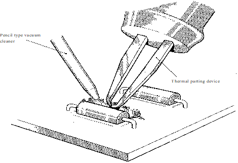 Figure: Removal of coating by thermal parting device
ANNEX(informative)Solder joint removal and unclinching
Introduction
A basic step for the repair of an electronic circuit is the removal of the solder joint retaining the component in position. There are various methods of achieving this and avoiding thermal and mechanical damage during component replacement. The following clauses describe a number of removal methods which can be used according to the facilities and the specific conditions.
Tools and materials
Soldering iron or hot jet blower (as applicable),
solder sucker: continuous vacuum device, hand, wicking wire (as applicable), and
thermal parting device, tweezers, pliers (as applicable).
Methods for solder joint removal and unclinching
Method for solder extraction with continuous vacuum
To obtain the continuous vacuum the operator either uses a vacuum pump or a separate vacuum device attached to the soldering iron. The solder can then be withdrawn from the joint either directly through the tip of the soldering iron or through a separate vacuum device attached to the soldering iron. The heated tip of the iron is applied to the soldered joint and, when a melt is noted, the vacuum is activated, e.g. by means of a foot switch, causing the solder to be withdrawn from the joint and deposited into a collecting chamber.
With appropriate handling, this method will minimise the overheating problem. The correct positioning of the vacuum device tip is shown in Figure B-1.
 Figure: Continuous vacuum solder extraction on stud lead
Method for solder extraction using sucker
This is a method in which the molten solder is removed by means of a sucker tip. There are several variations of this technique, but all of them have the disadvantage that the vacuum is applied only in short pulses and the procedure may have to be repeated several times. In addition, since the work is performed with two different devices simultaneously, i.e. soldering iron and sucker tip (refer to Figure B-2), this method finds only limited use.
 Figure: Pulsetype solder sucker in use
Method for hot jet extraction
This method relies on a thin jet of heated air (200 C to 300 C) to melt the defective solder joint. It is well suited to circuits in flat packages. Owing to the controlled dimensions of the jet, one can unsolder connecting wires individually without affecting the other joints. The molten solder is then wicked off or vacuumed away (refer to Figure B-3). This method finds only limited use.
 Figure: Lifting individual leads with hot jet
Method for the use of wicking braid
This method (refer to Figure B-4) incorporates braiding saturated with flux or stranded wire heated in contact with the solder joint. Capillary action causes the molten solder to be drawn into the wick. This method works well on large surface joints and can be applied to throughhole solder joints or, with more difficulty, to the solder between a clinched lead and a terminal area. As the amount of wickedout solder increases, the capillary action becomes less effective. Thus, joints containing a large amount of solder often require the repeated application of heat, creating a danger of overheating.
 Figure: Crosssectional view of wicking method
Method for unclinching of leads
Initial solder removal: first use method B.3.1 (Vacuum) or method B.3.4 (Wicking) to remove at least the surface solder from around the clinched lead and terminal area. This permits observation of the true circumstances of the clinched lead contact to the terminal area and the extent of the remaining solder joint between them.
After solder removal from the clinched area, the joint is allowed to cool down for a few seconds and the wire is carefully lifted with a thin plastic rod or similar device. The method, shown in Figure B-5, is designed to prevent damage to the terminal area. In lieu of the thermal parting device, tweezers or pliers may be used, provided that no contact is made with the terminal area.
Final solder removal: once the clinched leads are straightened, one may proceed to remove the solder joints by method B.3.1, treating them as if they were originally unclinched leads.
 Figure: Hot unclinching with thermal parting device
ANNEX(informative)Repair of damaged goldplated areas
Introduction
Goldplating can be damaged as a result of:
solder splatter on gold plating;
uneven scratched plating.
Tools and materials
Soldering iron,
solder sucker, wicking wire, penciltype vacuum cleaner,
safety glasses (or similar protecting device),
rubber gloves,
glass fibre eraser,
cleaning tissue, and
approved solvent.
Methods for the repair of damaged goldplated areas
Method for the removal of solder splatter on gold plating
Remove solder by vacuuming or by wicking with a flux impregnated wire (refer to method B.3.1 or B.3.4). Apply heat just long enough for melting and removal of the solder.
Remove remaining solder with a glass fibre eraser or similar and employing a vacuum cleaner.
Clean repair area with approved solvent.
ANNEX(informative)Repair of damaged conductor tracks
Introduction
The damage to the conductor can be in one of the following forms:
complete break;
scratches or nicks that reduce the currentcarrying capacity of the conductor to levels below standard requirement.
Tools and materials
Soldering iron and solder,
Tweezers,
Epoxy resin,
Approved solvent,
Fibre eraser,
Cleaning tissue.
Method for the repair of damaged conductor tracks
Clean both sides of break in conductor, to at least three times the track width on each side, with a fibre eraser and then with an approved solvent.
Cut a piece of applicable gauge tinned copper or silver wire to at least six times the track width.
Hold the wire with a pair of tweezers on centre line of conductor and solder in place.
Clean area with approved solvent.
Flow a small amount of epoxy resin over the entire repair and cure. Alternative coatings according to disposition by NRB may be used.
ANNEX(informative)Repair of lifted conductors
Introduction
This procedure is applicable where a portion of the conductor has lifted from the substrate but not broken (refer to Figure E-1).
 Figure: Lifted conductors
Tools and materials
Approved solvent,
spaceapproved epoxy adhesive (compatible with base epoxy),
plastic or wooden toothpicks,
strip of thin PTFE sheet,
small weights.
Methods for repair of lifted conductors
Method for the use of epoxy under conductor
(Refer to Figure E-2)
Clean underside of lifted conductor and surrounding area with an approved solvent.
Remove all particles that prevent the lifted conductor from making intimate contact with the surface of the substrate.
Using a hot air lance, gently blow the adhesive under the entire length of lifted conductor. Ensure the epoxy does not come into contact with surfaces required subsequently for soldering.
Press conductor into contact with substrate by the application of small weights; cover the interface between the weights and track with a thin piece of PTFE. Cure in conformance with the manufacturer data sheet
Do not handle repaired units until the epoxy has cured.
 Figure: Repair using epoxy under conductor
Method for the use of epoxy over conductor
(Refer to Figure E-3)
Clean the upper face of the lifted conductor and surrounding area with an approved solvent
Apply epoxy to the surface of the lifted conductor and to its surroundings to a distance of at least 3 mm in all directions from the damaged area.
Cure in conformance with the manufacturer data sheet.
Do not handle repaired units until the epoxy has cured.
 Figure: Repair using epoxy over conductor
ANNEX(informative)Repair of lifted terminal areas (pads)
Introduction
This procedure is applicable to:
any terminal area that has been separated, loosened or lifted or which is otherwise no longer bonded to the base material, as shown in Figure F-1;
any terminal area that has been damaged by tearing, cutting, or other mechanical means in excess of established acceptance limits (refer to Figure F-2 and Figure F-3);
terminal areas designed to accommodate clinched leads.
 Figure: Lifted terminal area
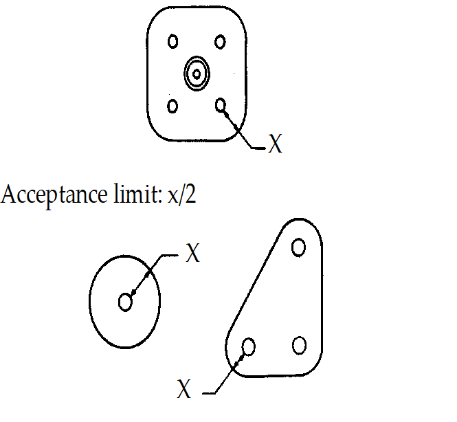 Figure: Terminal areas without track
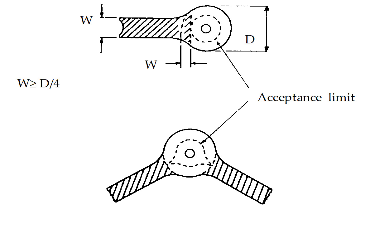 Figure: Terminal areas with track attached
Tools and materials
Solder remover (vacuum type),
oven (if thermal curing epoxy is used),
soldering iron,
plastic or wooden toothpicks (for lifting terminal area whilst cleaning),
approved solvent,
spaceapproved epoxy resin compatible with base epoxy,
weights.
Method for the repair of lifted terminal areas (pads)
Clean all dirt, fingerprints, flux residue and foreign matter from under and around pad with isopropyl alcohol or other approved solvent.
Insert spaceapproved epoxy adhesive under the copper with a camelhair brush, syringe or other suitable applicator.
Clean solder side of repair of terminal area.
Press terminal area down with a clamp or weight unit set.
Air cure or bake to manufacturer’s instructions before attempting further work.
ANNEX(informative)Terminal post replacement
Introduction
This procedure is applicable when terminal posts have become damaged.
Tools and materials
Replacement terminal posts,
side cutters,
soldering iron,
approved solder,
approved solvent,
appropriate PCB drill bits,
suitable support jigs,
pliers,
pencil vacuum cleaner.
Method for the replacement of terminal post
Remove the conformal coating from the area surrounding the damaged post (see clause 4.6).
Remove the component connected to the terminal post by cutting the component leads. Remove the section of component lead remaining at the nondamaged side of the component using the method described in Annex J.
Turn the printed circuit assembly over and support it on suitable jigging so that the subsequent drilling operation does not cause flexing of the assembly.
Select a drill bit that is approximately 80 % of the post diameter and drill into the post to a depth that just exceeds the thickness of the epoxy board (refer to Figure G-1).
With a drill bit the exact size of the terminal post, slowly drill into the post until the swaged section has been removed (refer to Figure G-1).
Remove the solder from the base of the post.
Take the post between the jaws of a pair of pliers and, with a slight rocking motion, pull the post from the printed circuit assembly. Apply heat if the terminal post is installed in a platedthrough hole.
Clean the surrounding area with approved solvent and pencil vacuum cleaner.
Fit replacement terminal post in conformance with normal manufacturing procedure.
Clean with approved solvent.
Inspect joint for correctness of swage and soldering.
Fit new component.
Reapply conformal coating to the area.
On PCBs with more than 2 layers and PTHs make sure that the internal layers are still connected.
 Figure: Terminal post replacement
ANNEX(informative)Wiretowire joints
Introduction
Wiretowire joints are used for wires that are broken or require lengthening for modification purposes.
Tools and materials
Side cutters,
soldering iron, solder and flux,
heating means (infrared or hot air),
approved solvent,
wire stripper,
heat shunt,
heat shrink sleeving (transparent, approved type),
approved insulated wire,
wire clamping device and
cotton gloves or finger cots.
Method for wiretowire joining
Cut wires to the correct length.
Remove wire insulation as detailed in clause 9.9.2 of ECSS-Q-ST-70-08 and ensure that the insulation clearance is as prescribed in clause 7.2.1.4 of ECSS-Q-ST-70-08.
If disturbed, restore the lay of a stranded conductor. Do not use bare fingers to achieve this.
Pretin the wires in conformance with clause 7 of ECSS-Q-ST-70-08.
Place heatshrink sleeving over the wire insulation in readiness for sliding over the joined wire.
If necessary, position wires into joined configuration and maintain position with clamping device (refer to Figure H-1).
Solder wires together (using heat shunt on each lead) to form a laptype joint. Ensure a low contact angle between the solder and wires and ensure that the contour of the individual conductor wires is visible.
Clean area with approved solvent to remove flux.
Inspect joint in conformance with clause 12 of ECSS-Q-ST-70-08.
Position shrink sleeve over joint and shrink to size in conformance with manufacturer’s instructions. Ensure that the shrink temperature is always below the melting point of the solder. For the configurations described in clauses Annex I and Annex L, a wraparound joint can be used for component lead extension.
Position the extended wire on the board and bond to the board using a suitable spaceapproved adhesive. Bond the lead along its length at intervals of not more than 2,5 cm. Make the first spot bond of the extension wire within 1,5 cm from the componenttowire soldered joint.
 Figure: Use of approved type support clamp/heat sink
ANNEX(informative)Addition of components
Introduction
Additional components can be required on a printed circuit assembly for the following reasons:
an oversight in design;
subsequent testing of the manufactured assembly indicates a need for modification;
a change in the design requirement.
Tools and materials
Soldering iron,
approved solder,
side cutters,
heat shunt,
wire stripper,
approval solvent and cleaning brushes,
approved epoxy paste staking compound,
approved thixotropic polyurethane staking compound,
terminal pins,
wire insulation,
approved insulated wire,
lintfree paper, and
pencil type vacuum cleaner.
Methods for addition of components
Method for additional components mounted on reverse (noncomponent) side of board
Using lintfree paper, mask as much as possible of the circuitry surrounding the area to be worked.
Carefully remove any conformal coating from the area to be worked. Use the method described in Annex A.
If the new component lead traverses conductors, assemble insulating sleeving to the section of lead that will not be soldered (refer to Figure I-1).
Form the component lead as shown in Figure I-1. Form the section of lead to be soldered so that it follows the centreline of the conductor track. Observe forming in conformance with clause 8.1.5 of ECSS-Q-ST-70-08.
Use component lead diameter (or width) less or equal to two thirds of track width.
Solder into position.
Remove protective paper.
Clean soldered area with approved solvent.
Inspect with respect to clause 8.1.5 of ECSS-Q-ST-70-08 .
Reapply conformal coating and cure in conformance with the manufacturer data sheet
 Figure: Additional components mounted on reverse (noncomponent) side of board
Method for additional components mounted on component side of board
Using lintfree paper, mask as much as possible of the circuitry surrounding the area to be worked.
Carefully remove any conformal coating from the area to be worked. Use the method described in Annex A.
Drill holes in the printed circuit assembly adjacent to the conductor tracks to which the component is to be joined. Use the vacuum cleaner during this operation to remove swarf. Drill holes with diameters which are of the size component lead diameter, plus 0,25 mm to 0,50 mm. Position the hole that the edge of the hole is a minimum of 0,2 mm from the edge of the conductor.
Form the component leads and assemble the component to the board as shown in Figure I-2. Components may also be mounted parallel with existing tracks to avoid additional bending of leads. Consider the stress relief and bend radius requirements of clause 8.1.5 in ECSS-Q-ST-70-08.
Place the section of the component lead to be soldered along the centre line of the conductor and solder into this position (refer to Figure I-2).
Use component lead diameter (or width) less or equal to two thirds of track width.
Clean soldered area with approved solvent.
Inspect in conformance with clause 8.1.5 of ECSS-Q-ST-70-08.
Reapply conformal coating and cure according to the manufacturer data sheet
 Figure: Additional components mounted on component side of board
Method for additional components mounted on terminal posts, including “piggyback“ mounting
Using lintfree paper, mask as much as possible of the circuitry surrounding the area to be worked.
Carefully remove any conformal coating from the area to be worked. Use the method described in Annex A.
Drill the terminal post holes into suitable land areas of the conductor track. Use the vacuum cleaner during this operation.
Mount and solder the terminal posts in their respective holes.
Solder the component to the terminal posts in conformance with clause 9 ECSSQ-ST7008.
If it is necessary to attach the leads of the component to the noncomponent side of the board, use method I.3.2 step c. Mount components parallel to each other with one side of each component lying on the PCB. However, it is also permissible to mount one component on top of another (“piggyback” mounting). If this is required, solder the second component to the terminal posts as shown in Figure I-3.
For a “piggyback” configuration, apply an approved staking compound to join component bodies together and the lower component to the board.
Reapply conformal coating and cure according to the manufacturer data sheet
 Figure:“Piggyback” mounting of one component on top of another
Method for additional components mounted (on reverse side or on component side of board) using staking compound
The bonding of components avoids subsequent vibration problems. Several configurations are permissible (refer to Figure I-4, Figure I-5, Figure I-6, and Figure I-7).
Using lintfree paper, mask as much as possible of the circuitry surrounding the area to be worked.
Carefully remove any conformal coating from the area to be worked. Use the method described in Annex A.
For the configuration shown in Figure I-7 only, drill holes in the doublesided printed circuit board at the position where the component is to be mounted. Use the vacuum cleaner during this operation to remove swarf. Drill holes with diameters which are of the size component lead diameter, plus 0,25 mm to 0,50 mm. This procedure can be applied to multilayer boards, if controls are applied to ensure that internal conductors are not damaged.
Form the component leads. Bond the component to the board with epoxy paste or thixotropic polyurethane staking compound as illustrated in Figure I-4, Figure I-5, Figure I-6, and Figure I-7. Cure according the manufacturer data sheet.
If a DIL package is mounted upside down, degold and pretin leads in conformance with clause 7.2.3 of ECSS-Q-ST-70-08. Re-mark part coding onto the underside to preserve identification.
Consider the stress relief and bend radius requirements (clause 8.1.5 of ECSS-Q-ST7008).
Strip, pretin (with use of a heat sink to prevent wicking) and form spaceapproved insulated wire for component lead extension.
For connecting top/bottom sides of doublesided or multilayer printed circuit boards, insulated wire can be passed through unused plated through holes. Holes should not be drilled or solderwicked to enable the wire to be inserted. (AWG 30, silver plated, stranded, insulated wire fits adequately in a plated through hole of diameter 0,75 mm).
Solder wires to component leads using a wraparound connection as per clause “Turret and straight pin terminals” of ECSS-Q-ST-70-08 (refer to Figure I-4, Figure I-5,Figure I-6, and Figure I-7).
For some component types, use a heat sink to prevent reflow of low melting point soldered connections within the component body.
Clean soldered area with approved solvent.
Inspect in conformance with clause 12 of ECSS-Q-ST-70-08.
Position wire extensions on board and bond to the board in conformance with Annex H.
Reapply conformal coating and cure according to the manufacturer data sheet
Method for additional components mounted (on reverse side or on component side of board) to leads of adjacent components
Different configurations in conformance with the Figure I-8, Figure I-9, and Figure I-10 may be used.
Using lintfree paper, mask as much as possible of the circuitry surrounding the area to be worked.
Carefully remove any conformal coating from the area to be worked. Use the method described in clause Annex A.
For the configurations shown in Figure I-8 and Figure I-9, remove existing components in the adjacent positions (to which connections of the additional component are required). Use the method described in Annex J. Replace with new components which have either leads extended in the “Z” direction (refer to Figure I-8) or a formed “pigtail” lead (refer to Figure I-9).
Form the leads of the additional component. Consider the stress relief and bend radius requirements (clause 8.1.5 of ECSS-Q-ST-70-08. For the configuration shown in Figure I-10, assemble insulating sleeving to the section of lead that will not be soldered if lead passes above a conductor.
Solder leads onto the leads of adjacent components using a wraparound connection as per clause “Turret and straight pin terminals” of ECSS-QST7008.
Clean soldered area with approved solvent.
Inspect in conformance with clause 12 of ECSS-Q-ST-70-08.
For the configurations shown in Figure I-9 and Figure I-10, bond components to the board.
Reapply conformal coating and cure in conformance with the manufacturer data sheet
 Figure: Mounting and wiring of additional axiallyleaded components mounted (on reverse side or on component side of board) using staking compound
 Figure: Upside down mounting and wiring of additional sidebrazed DIL component (on reverse side or on component side of board) using staking compound
 Figure: Mounting of additional nonaxially leaded components, e.g. capacitors, with wire connecting top or bottom sides of the circuit board using staking compound (on reverse side or on component side of board)
 Figure: Mounting of additional component (on component side of board) with wire connections on reverse side of board using staking compound
 Figure: Mounting of additional component (on reverse side of board) across extended leads of adjacent components
 Figure: Mounting of additional component by linking to a “pigtailed” lead of an adjacent component
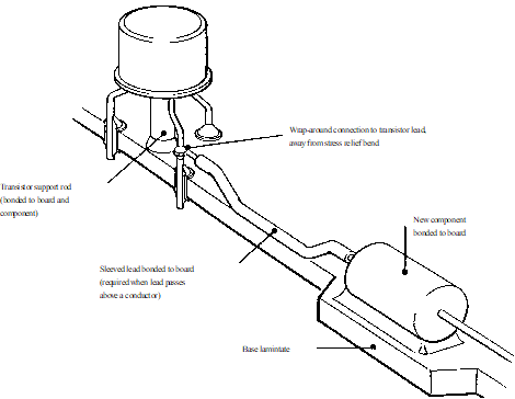 Figure: Mounting of additional component by linking to lead of an adjacent transistor (or other large component)
Method for the addition of a wire link onto soldered chips on a single side piece of PCB with appropriate pads
The number of pieces of PCB should not exceed two within any one area of 25 cm2. It is possible to glue a piece of PCB onto a tinned surface if this does not exceed 50 % of piece surface.
Glue with epoxy pieces of PCB on PCB board and cure.
Solder wire on appropriate pads on piece of PCB. With a length greater than 1,2 mm.
Clean soldered area with approved solvent.
Inspect joint in conformance with clause 12 ECSS-Q-ST-70-08.
Position the extended wire on the board and bond to the board by using a suitable spaceapproved adhesive (epoxy spot). Bond the lead along its length at intervals of not more than 3 cm, if it is longer than 3 cm. Make the first spot bond of the extension wire just after the wire stress relief.
Reapply conformal coating and cure in conformance with the manufacturer data sheet.
Method for the addition of a wire link onto metallized cap of chips directly glued on PCB
Put an epoxy spot at the centre of component, suited with the size of package.
Bond the chip on PCB and cure.
Check that the epoxy spot does not extend onto metallized cap.
Solder silver wires or insulated wire (refer to Figure I-11.
Clean soldered area with approved solvent.
Inspect in conformance with clause 12 of ECSS-Q-ST-70-08.
Position the extended wire on the board and bond to the board by using a suitable spaceapproved adhesive (epoxy spot). Bond the lead along its length at intervals of not more than 3 cm, if it is longer than 3 cm. Make the first spot bond of the extension wire just after the wire stress relief.
Reapply conformal coating and cure in conformance with the manufacturer data sheet.
 Figure: Addition of a wire link onto metallized cap of chips directly glued on PCB
ANNEX(informative)Removal and replacement of axial and multilead components
Introduction
This procedure is applicable to components having axial or multilead configurations.
Tools and materials
Sidecutting pliers or diamond saw,
soldering iron,
longnose pliers, and
approved solvent.
Methods for removal and replacement of axial and multilead components
Method for the removal of components with axial leads (destructive removal)
Cut the vertical section of the component leads just above the solder fillet and parallel to the surface of the board. Ensure that burrs are not formed.
Remove the remaining portion of the lead on the other side of the board using either a soldering iron with wick or vacuum extractor, then gently pull the lead with longnose pliers when the solder is molten.
Remove excess solder with a vacuum extractor or solder remover.
Clean up the area of the joint with an approved solvent.
Fit new component and solder it in place in conformance with clause 8 ECSSQ-ST-70-08.
Method for the removal of multilead components (destructive removal)
Cut component leads using diamond saw or sidecutting pliers (refer to Figure J-1 and Figure J-2).
Unsolder and remove the remaining portion of the leads on the other side of the board, whilst gently pulling with longnose pliers when the solder is molten.
Remove excess solder with a vacuum extractor or by the wicking method.
Clean the area of the joint with an approved solvent.
Fit new component and solder in place in conformance with clause 8 of ECSS-Q-ST-70-08.
 Figure: Removal of multilead components, clipping of component leads
 Figure: Removal of multilead components, removal of remaining component leads
ANNEX(informative)Removal and replacement of flatpack components
Introduction
This procedure is applicable to components in flatpack configuration mounted on the printed circuit board, in the same plane as the conductive pattern by means of lapsoldered joints.
Tools and materials
Soldering iron, heat controlled,
solder,
wicking braid,
strip Kapton or Teflon sheet (approx. 6 cm long),
leadbending fixture for flatpack circuits, and
approved solvent and cleaning tissue.
Method for the removal and replacement of flatpack components
Apply heat to the soldered joint, simultaneously lifting the leads by sliding a piece of thin Kapton or Teflon sheet progressively from the nonsoldered section of the lead towards the soldered section (refer to Figure K-1).
Remove adhesive bonding, if applicable, by suitable means as dispositioned by NRB.
Clean solder area using an approved cleaning solvent.
Inspect surface of joint for raised areas of track and overheated solder.Repair raised surfaces in conformance with the methods described in Annex E. Remove overheated solder by wicking and re-tin the solder area.
Position new component, tack it to the board for stability if required and solder in place using a heatcontrolled soldering iron. If package density allows, a reflow machine with a single lead tip (pegtip) may be used.
Apply new adhesive if required by component size, in conformance with the clause 8.1.2 of ECSS-Q-ST-70-08.
 Figure: Removal of flatpack components
ANNEX(informative)Modification of component connections
Introduction
Modification of the connections from components to the printed circuit board can be required for the same reasons as those given in clause I.1.
Tools and materials
Soldering iron,
approved solder,
side cutters,
approved solvent and cleaning brushes,
lintfree paper,
pencil type vacuum cleaner,
approved epoxy paste staking compound,
approved insulated wire,
plain copper wire,
Teflon sleeve tubing,
handheld drill,
scalpel blade, and
longnose pliers.
Methods for modification of component connections
Method for the soldering of a wraparound connection to an extended component lead
Using lintfree paper, mask as much as possible of the circuitry surrounding the area to be worked.
Carefully remove any conformal coating from the area to be worked. Use the method described in Annex A.
Remove existing component in the location at which a wrap around connection is required. Use the method described in Annex J. Replace with a new component with lead extended in the “Z”-direction (refer to Figure L-1).
Strip, pretin (with use of a heat sink to prevent wicking) and form spaceapproved insulated wire for wraparound connection to extended lead.
Solder wire to extended component lead using a wraparound connection as per clause “Turret and straight pin terminals” of ECSS-Q-ST7008.
Clean soldered area with approved solvent.
Inspect in conformance with clause 12 of ECSS-Q-ST-70-08.
Position wire connection on board and bond to the board as defined in Annex H.
Reapply conformal coating and cure in conformance with the manufacturer data sheet.
 Figure: Soldering of a wraparound connection to an extended component lead
Method for the soldering of component lead to a stud lead mounted into an existing hole
Pretin and solder a suitable diameter plain copper wire into the plated through hole.
Mount component by attaching component lead to stud lead using a wraparound connection (refer to Figure L-2) as per clause “Turret and straight pin terminals” of ECSS-Q-ST-70-08.
Clean soldered area with approved solvent.
Inspect in conformance with clause 12 of ECSS-Q-ST-70-08.
Ensure stress relief is provided in component lead.
 Figure: Soldering of component lead to a stud lead mounted into an existing hole
Method for mounting a dualinline (DIL) package with or without a wire link soldered onto a cropped lead
Using lintfree paper, mask as much as possible of the circuitry surrounding the area to be worked.
Remove the existing DIL package. Use the method described in Annex J.
As required, crop leads of a replacement component in line with the bottom of the component body as shown in Figure L-3. (The component may be of either a “J”lead or a “sidebrazed” lead configuration).
Degold and pretin the leads in two operations in conformance with clause 7 of ECSS-Q-ST-70-08. If connection of cropped leads to the board is required, then de-gold and pre-tin the cropped leads by hand. For cropped sidebrazed leads de-gold and pre-tin the entire lead shoulder (but this does not necessarily include the goldplating on the braze fillet).
Solder the replacement component into position. If no connection of cropped leads to the board is required, proceed to step h.
Strip, pretin (with use of a heat sink to prevent wicking) and form spaceapproved insulated wire for connection of cropped leads to board.
Solder wires to cropped leads to form a lap joint. Wires may be led down onto the board or may pass away from the board (refer to Figure L-3 and Figure L-4). Use the lap joint with a length of three times the stripped wire diameter. For cropped “J”leads, solder for not ore than 3 seconds at a tip temperature of (250 5) C. For cropped “sidebrazed” leads, solder for not more than 3 seconds at a tip temperature of (295 5) C.
Clean soldered area with approved solvent.
Inspect in conformance with clause 12 of ECSS-Q-ST-70-08. Position wire connections on board and bond to the board as defined in Annex H.
Reapply conformal coating and cure in conformance with the manufacturer data sheet.
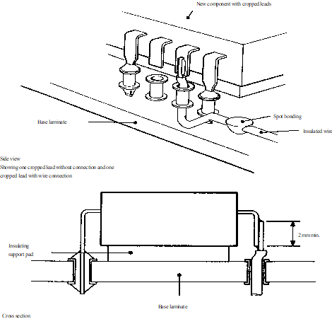 Figure: Mounting a dualinline package with or without a wire link soldered onto a cropped lead (cropped lead without connection and cropped lead with connection led through hole and onto board)
 Figure: Mounting a dualinline package with or without a wire link soldered onto a cropped lead (wire link passing away from board)
Method for mounting a connector with or without a wire link soldered onto a cropped lead
Using lintfree paper, mask as much as possible of the circuitry surrounding the area to be worked.
Remove the existing connector from the board. Use the method described in Annex J.
As required, crop leads of a replacement connector as shown in Figure L-5.
Degold and pretin connector leads, including cropped leads, if connection of cropped leads to the board is required.
Solder the replacement connector into position. If no connection of cropped leads to the board is required, proceed to step h.
Strip, pretin (with use of a heat sink to prevent wicking) and form spaceapproved insulated wire for connection of cropped leads to board.
Solder wires to cropped leads using a wraparound connection as per clause “Turret and straight pin terminals” of ECSSQST7008.
Clean soldered area with approved solvent.
Inspect in conformance with clause 12 of ECSS-Q-ST-70-08.
Position wire connections on board and bond to the board as defined in Annex H.
Reapply conformal coating and cure in conformance with the manufacturer data sheet.
 Figure: Mounting a connector with a wire link soldered onto a cropped lead
Method for the addition of a wire link into a platedthrough hole occupied by a flatsection lead
Volume limitations prevent the insertion of a wire link into a hole occupied by a roundsection lead.
Using lintfree paper, mask as much as possible of the circuitry surrounding the area to be worked.
Remove conformal coating from the area surrounding the plated through hole requiring addition of a wire link. Use the method described in Annex A.
Desolder the lead occupying the hole. Use the method described in Annex B.
Strip, pretin (with use of a heat sink to prevent wicking) and form spaceapproved insulated AWG 30 wire for making a link into the plated through hole.
Insert wire into plated through hole to lie alongside the existing component lead. The wire may enter from either the reverse side of the board (refer to Figure L-6) or from the component side of the board (refer to Figure L-7). Solder wire or component lead into place. (Figure L-6 and Figure L-7 illustrate the solder fillet to be achieved).
Clean soldered area with approved solvent.
Inspect in conformance with clause 12 of ECSS-Q-ST-70-08.
Position wire link on board and bond to the board as defined in Annex H.
Reapply conformal coating and cure in conformance with the manufacturer data sheet
 Figure: Addition of a wire link into a plated through hole occupied by a flatsection lead (wire link entering from the reverse side of the board)
 Figure: Addition of a wire link into a plated through hole occupied by a flatsection lead (wire link entering from the component side of the board)
Method for the addition of a wire link on top of a flatpack lead
Using lintfree paper, mask as much as possible of the circuitry surrounding the area to be worked.
Remove conformal coating from the area surrounding the flatpack lead requiring addition of a wire link. Use the method described in Annex A.
Strip, pretin (with use of a heat sink to prevent wicking) and form spaceapproved insulated wire for making a link on top of the flatpack lead.
Place the section of the wire to be soldered along the centre line of the lead and solder into this position (refer to Figure L-8 and, for the solder fillet appropriate for a lap joint, Figure I-1 and Figure I-2). Use a wire with diameter less or equal to two thirds lead width.
Clean soldered area with approved solvent.
Inspect in conformance with clause 12 of ECSS-Q-ST-70-08.
Position wire link on board and bond to the board as defined in Annex H.
Reapply conformal coating and cure in conformance with the manufacturer data sheet .
 Figure: Addition of a wire link on top of a flatpack lead
Method for the isolation of a component lead
This “drillingisolation” method is critical.
Using lintfree paper, mask as much as possible of the circuitry surrounding the area to be worked.
Remove the existing component. Use the method described in Annex J.
Where isolation is required, drill out plated through holes, using a handheld drill. Hold the drill vertically with respect to the board. For example, a 1,1 mm diameter drill can be used for a 0,75 mm diameter hole.
Remove pads on both sides of the board using a new scalpel blade. Take care that no glass fibres within the board are cut.
Drill out further. For example, after using a 1,1 mm diameter drill (refer to step c.) use a 1,3 mm diameter handheld drill. Use the vacuum cleaner to remove swarf from the drilling operations.
Insert lengths of Teflon sleeve tubing into drilled out holes so that the tube isolates the lead between component body and soldering spot in such a way that a minimum distance of 0,5 mm is achieved (refer to Figure L-9). (For the example above, use tubing of 0,5 mm internal bore diameter).
Insert new component with appropriate leads passing through the isolated holes. Solder remaining leads.
When required, attach stripped, pretinned and formed insulated wire to the isolated lead using a wraparound connection as per clause “Turret and straight pin terminals” of ECSS-Q-ST-70-08.
Clean soldered area with approved solvent.
Inspect in conformance with clause 12 of ECSS-Q-ST-70-08
Spot bond component and wire connections using epoxy staking compound and cure in conformance with standard requirements.
Reapply conformal coating and cure in conformance with the manufacturer data sheet .
 Figure: Isolation of a component lead
Method for the addition of a wire link onto terminal pad of soldered chips
Flux the chip solder joint with brush.
Solder silver wires or insulated wires (refer to Figure L-10) over a length greater than 1,2 mm.
Clean soldered area with approved solvent.
Inspect joint in conformance with clause 12 of ECSS-Q-ST-70-08.
Position the extended wire on the board and bond to the board by using a suitable spaceapproved adhesive (epoxy spot). Bond the lead along its length at intervals of not more than 3 cm, if it is longer than 3 cm. Make the first spot bond of the extension wire just after the wire stress relief.
Reapply conformal coating and cure in conformance with the manufacturer data sheet.
 Figure: Addition of a wire link onto terminal pad of soldered chips
ANNEX(informative)Cutting of internal track of a multilayer printed circuit board
Introduction
This procedure can be used when it is necessary to interrupt an internal connection of a multilayer printed circuit board.
Tools and materials
Lintfree paper,
approved solvent and cleaning brushes,
pencil type vacuum cleaner,
approved PCB repair facility (work station), including a milling attachment, and
approved epoxy compound.
Method for cutting the internal track of a multilayer printed circuit board
Using lintfree paper, mask as much as possible of the circuitry surrounding the area to be worked.
Carefully remove any conformal coating from the area to be worked. Use the method described in clause Annex A.
Mill through successive layers of the board progressively (to ensure clear visibility of layer separation and to avoid the presence of shorts caused by burrs) until there is clear visibility of the internal track to be cut (refer to Figure M-1). Use the vacuum cleaner to remove swarf from the milling operation.
Cut the track and check that the resistance is greater than 2 M.Ensure there is no damage to mounted parts during electrical monitoring.
Remove protective paper.
Clean milled area with approved solvent.
Fill hole with epoxy compound and cure to the manufacturer data sheet
Reapply conformal coating and cure to the manufacturer data sheet.
 Dimensions are for guidance only
Figure: Cutting of internal track of a multilayer circuit board
Bibliography
|
ECSS-S-ST-00
|
ECSS system — Description and implementation and general requirements
|