
Space engineering
ASIC, FPGA and IP Core engineering
Foreword
This Standard is one of the series of ECSS Standards intended to be applied together for the management, engineering, product assurance and sustainability in space projects and applications. ECSS is a cooperative effort of the European Space Agency, national space agencies and European industry associations for the purpose of developing and maintaining common standards. Requirements in this Standard are defined in terms of what shall be accomplished, rather than in terms of how to organize and perform the necessary work. This allows existing organizational structures and methods to be applied where they are effective, and for the structures and methods to evolve as necessary without rewriting the standards.
This Standard has been prepared by the ECSS-E-ST-20-40C and ECSS-Q-ST-60-03C Working Group, reviewed by the ECSS Executive Secretariat and approved by the ECSS Technical Authority.
Disclaimer
ECSS does not provide any warranty whatsoever, whether expressed, implied, or statutory, including, but not limited to, any warranty of merchantability or fitness for a particular purpose or any warranty that the contents of the item are error-free. In no respect shall ECSS incur any liability for any damages, including, but not limited to, direct, indirect, special, or consequential damages arising out of, resulting from, or in any way connected to the use of this Standard, whether or not based upon warranty, business agreement, tort, or otherwise; whether or not injury was sustained by persons or property or otherwise; and whether or not loss was sustained from, or arose out of, the results of, the item, or any services that may be provided by ECSS.
Published by: ESA Requirements and Standards Section ESTEC, P.O. Box 299, 2200 AG Noordwijk The NetherlandsCopyright: 2023© by the European Space Agency for the members of ECSS## Change log
|
ECSS-E-ST-20-40C
|
First issue
|
Introduction
Developing custom designed monolithic integrated circuits such as ASICs or FPGAs, and developing IP Cores, as off-the-shelf Building Blocks for these complex ICs, make certain engineering and technical management activities crucial to the success of these developments.
ECSS-E-ST-20-40 was written in parallel and in co-ordination with the writing ECSS-Q-ST-60-03, by the same ECSS Working Group. These two new and complementary standards cover respectively the engineering and the product assurance requirements to be applied when developing ASICs, FPGAs and IP Cores, and these two new standards together supersede ECSS-Q-ST-60-02C.
The DEVICE qualification status is assessed based on the requirements from both ECSS-E-ST-20-40 and ECSS-Q-ST-60-03. In order for a DEVICE to be qualified and accepted according to ECSS standards, the DEVICE development reviews defined in ECSS-E-ST-20-40 have to be declared successful by the customer engineering and PA responsible persons and project management who monitored the DEVICE development.
Scope
This standard defines a comprehensive set of engineering requirements for the successful development of digital, analogue and mixed analogue-digital signal custom designed integrated circuits, such as application specific integrated circuits (ASICs), field programmable gate arrays (FPGAs) and Intellectual Property Cores (IP Cores), from now on referred to with the single and generic term DEVICEs.
Microelectronics systems created by more than one DEVICE die but that are interconnected and packaged together as a single DEVICE are not considered single monolithic DEVICEs. However ECSS-ST-20-40 is to be applied to (a) the development of each individual monolithic die, (b) also for their integration onto a multi-die single DEVICE considering those dice as IP Cores.
This standard may be tailored for the specific characteristic and constraints of a space project in conformance with ECSS-S-ST-00. A pre-tailoring based on the actual DEVICE type and criticality category of the DEVICE is addressed in clause 5.1.2.This standard does not cover requirements for the selection, control, procurement or usage of DEVICEs for space projects nor DEVICE ESCC qualification requirements, as those requirements are covered by ECSS-Q-ST-60C EEE components standard and the ESCC generic specification No. 9000 respectively. Nevertheless, this standard contemplates the possibility for the DEVICE to undergo ESCC qualification after the DEVICE customer acceptance as an ECSS qualified DEVICE, and thus a DEVICE ESCC Detail Specification and DEVICE Radiation Test Plan and Report are optional expected outputs.### Normative references
The following normative documents contain provisions which, through reference in this text, constitute provisions of this ECSS Standard. For dated references, subsequent amendments to, or revisions of any of these publications do not apply. However, parties to agreements based on this ECSS Standard are encouraged to investigate the possibility of applying the most recent editions of the normative documents indicated below. For undated references the latest edition of the publication referred to applies.
|
ECSS-S-ST-00-01
|
ECSS system – Glossary of terms
|
|
ECSS-Q-ST-30
|
Space product assurance – Dependability
|
|
ECSS-Q-ST-40
|
Space product assurance – Safety
|
|
ECSS-Q-ST-60-03
|
Space product assurance – ASIC, FPGA and IP Core product assurance
|
Terms, definitions and abbreviated terms
Terms from other standards
For the purpose of this Standard, the terms and definitions from ECSS-SST0001 apply, in particular the following terms:
- acceptance
- component
- customer
- engineering model
- flight model
- informative
- maintenance
- model
- normative
- performance
- project
- requirement
- risk
- supplier
The old term firmware is defined in ECSS-S-ST-00-01C, and it is not used in the context of ECSS-E-ST-20-40 because with the emergence of new technologies it is now ambiguous and unnecessary. It is important not to confuse terms like FPGA, FPGA programming file or FPGA programming bit stream with firmware.
Terms specific to the present standard
Application Specific Integrated Circuit
full custom or semi custom designed monolithic integrated circuit
ASICs can be digital, analogue or a mixed function.
block diagram
abstract graphical presentation of interconnected named boxes or blocks representing an architectural or functional drawing
Building Block
reusable IC design element that implements a self-standing function or group of functions for which ownership rights exist and that has been developed in the context of a specific IC project or technology, without the intention to be shared with third parties for its reuse in other IC projects
For example, an HDL model such as synthesizable VHDL code, or gate-level netlist, or an analogue function.
cell
specific circuit function including digital or analogue basic blocks
cell library
collection of all mutually compatible cells which conforms to a set of common constraints and standardized interfaces designed and characterized for a specified technology
code
string of words, numbers, letters and symbols that is used to model a DEVICE or its verification and validation environment
For example, Hardware Description Languages like VHDL, Verilog or System-C are used to code DEVICE behavioral or synthesisable models, and code in other languages like C, Python or Tool Command Languages (Tcl) can be used in the DEVICE verification and validation.
data sheet
detailed functional, operational and parametric description of a DEVICE
A data sheet can include, for instance, a block diagram, truth table, pin and signal description, environmental, electrical and performance parameters, tolerances, timing information, and package description.
design for test
technique used to allow a complex integrated circuit to be tested with respect to potential manufacturing faults or to accelerate otherwise too slow validation tests
- 1 For example, any dedicated circuits aimed to provide better observability or commandability of internal nodes of the DEVICE not accessible through primary inputs and outputs.
- 2 Other examples of DFT are test busses, boundary scan as in JTAG, see IEEE 1149.1-2013, built-in self-test, and test modes for functional tests performed at DEVICE Validation, Qualification and Acceptance Phase.
design iteration
design changes that occur in any single phase or between two consecutive phases as defined in the DEVICE Development Plan, before the final DEVICE is released
DEVICE
integrated circuit or an IP Core
-
1 A DEVICE can be a digital, analogue or mixed-signal ASIC, a programmed FPGA, a blank FPGA, a microprocessor, and a model of an IC function that is conceived for reuse as an IP Core.
-
2 A DEVICE can also be a group of dice or chiplets interconnected and integrated inside a single package, such as a system-in-package or a multi-chip-module.
DEVICE Database
set of all digital files that are needed for the development of a DEVICE -
1 Examples of files integrating this database are behavioral and HDL models of the DEVICE, layout description files, models of the DEVICE system environment used to verify by simulation the DEVICE functionality, configuration files and SW programs used for the automation of the verification and validation of the DEVICE, input and output files used and generated by the different CAD tools used, for example files describing the resources, area, timing and power constraints, stimuli and expected output values files, or FPGA bit stream binary files.
-
2 This database of files is incrementally updated throughout the DEVICE development phases, and all necessary elements that enable support, maintenance and a new development of the same or a modified version of the DEVICE can be found in the DEVICE database at the end of the DEVICE Validation, Qualification and Acceptance Phase.
DEVICE development flow
selection and sequence of engineering methods and tools applied during the definition, design, verification, implementation and validation of the DEVICE
DEVICE model
textual or graphical representation of a DEVICE, or a part of it, which defines one or several DEVICE characteristics
-
1 For example, digital or analogue functional behavior, timing performance, power consumption, sizes and interconnections of physical internal structures, input and output external interfaces, environmental effects due to temperature, radiation or aging.
-
2 DEVICE models can be created graphically as graphical design drawings or with textual Hardware Description Languages like VHDL, Verilog, System-C or EDIF.
-
3 DEVICE models can implement several levels of abstraction such as behavioral, Register-Transfer-Level, gate-level netlist or transistor-level, and accuracy such as untimed, loosely timed or approximately timed.
-
4 DEVICE models can be generated manually, assisted by CAD specialized IC design tools or a mix of both.
DEVICE technology
totality of all elements needed for the design, physical implementation and test of either ASIC or FPGA components -
1 For example, design tools and their description, cell libraries, procedures, design rules, manufacturing process, programming tools, test equipment
-
2 Sometimes the terms ASIC technology or FPGA technology are used when referring to the technology of only that type of DEVICE
fault coverage
measure expressed as a percentage of the proportion of actually detectable faults versus all possible faults in a digital circuit, for a given set of test patterns and with respect to a specific fault model
Field Programmable Gate Array
standard semiconductor device that becomes customized when programmed by the user with specific software and hardware tools
FPGA Programming Test
test performed to validate the successful programming of an FPGA
For example, to detect inaccurate programming procedures, incorrect programming files, poor calibration of FPGA programmer, or material defects in the FPGA.
floorplan
abstracted, scaled layout drawing of the die, outlining the form, size and position of the major functional blocks and the pads including power and ground lines, clock distribution and interconnect channels
HDL model
textual description of an integrated circuit based on a hardware description language suitable for the behavioural or structural description and simulation
IP Core
integrated circuit design element that implements a self-standing function or group of functions for which ownership rights exist and is developed for reuse and released with comprehensive verification, validation and documentation
- 1 IP core can be acquired by a customer, for a given price and under an owner-defined license agreement specifying the customer's acquired rights.
- 2 IP core can be supplied as an HDL model, as a synthesizable VHDL code or gate-level netlist, and with the essential complementary documentation that allows the customer to successfully integrate and use it in a system for example User’s Manual and verification files. From this point of view, it can be seen as a semi-finished product.
- 3 IP Cores can be analogue functions provided by DEVICE technology providers as macrocells.
- 4 In contrast with Building Blocks, IP Cores have gone through comprehensive verification, validation and documentation intended for reuse of third parties.
- 5 IP Cores sometimes are referred as hard IPs if they are already placed and routed for one specific IC technology. For example, a macrocell already pre-diffused inside an FPGA or an already layouted function that is included in an ASIC, or a netlist that cannot be modified and is treated as a black-box.
- 6 An IP Core can be composed by combination of different IP Cores.
macrocell
module that contains complex functions in a given technology’s cell library built up out of hard-wired primitive cells
Macrocells can be provided as a library component for ASIC design, for example RAM blocks, or be present inside pre-diffused devices such as DSP blocks or microprocessor cores existing inside FPGAs.
netlist
formatted list of cells, basic circuits, and their interconnections
-
1 The term pre-layout netlist is used for DEVICE netlists that do not contain yet the DEVICE layout information. For example, detailed timing behavior of the cells, timing impact of the interconnections.
-
2 For FPGA, pre-layout netlist means usually the netlist obtained through synthesis tools.
phase
set of interrelated DEVICE development activities -
1 A DEVICE generic development flow usually consists of seven phases as depicted in Figure 51. See Annex J for more development flow examples.
-
2 The concept of phase is equivalent to the concept of process defined in ECSS-S-ST-00-01.
processing unit
function which is defined to execute software -
1 The term covers hardware functions such as general purpose processing cores, and more specialized Graphical Processing Unit (GPU), Vision Processing Unit (VPU), Tensor Processing Unit (TPU), Neural Processing Unit (NPU), Physics Processing Unit (PPU), Digital Signal Processor (DSP), or Image Signal Processor (ISP).
-
2 In the context of SW engineering, it also covers software processing units such as interpreters, emulators and virtual machines.
Production Test
test performed on the manufactured DEVICEs to detect functional problems resulting from faults or random material defects during wafer manufacturing, die assembly and packaging -
1 Production Tests are normally performed with test vectors generated by the DEVICE designer and Automatic Test Equipment (ATE) by the DEVICE manufacturer.
-
2 Production Tests include for example stuck-at faults scan tests, timing delay faults, I/O parametric tests for digital ASICs.
-
3 Analogue ASICs Production Tests examples are reference voltage or current tests, AD/DA converters tests or tests to catch manufacturing defects affecting any analogue function.
-
4 Production Tests are not DEVICE Validation tests, which are tests performed on the final DEVICE, ASIC or FPGA, to validate that all requirements in DRS are met. Validation tests are normally performed by the DEVICE development team (the supplier), and not by the DEVICE manufacturer (the foundry), and they include functional, environmental and mechanical tests.
prototype
fabricated ASIC or programmed FPGA used to verify preliminary implementations of the DEVICE against the DEVICE Requirements Specification
redesign
design changes which were not planned in the DEVICE Development Plan and which involve reopening an already closed phase
These design changes can be motivated by unexpected changes in the DRS, wrong interpretation of the DRS or design mistakes.
software
set of instructions and data executed on a processing unit
- 1 A processing unit can be hardware, for example a processor chip, or software, for example a virtual machine or an interpreter.
- 2 Some processing units only require data, for example configuration of state machines or configuration data of a neural network.
- 3 Files using Hardware Description Languages (VHDL, Verilog, System-C) used to model ASICs or bit stream files used to program FPGAs are not software.
stimuli
input data set for simulation or test to show a specific functionality or performance of a DEVICE
synthesis tool
tool that automatically converts a high-level textual representation of an integrated circuit, usually coded in Hardware Description Language at register–transfer-level, into an optimized gate-level netlist representation of the integrated circuit
system requirement
functional, electrical, environmental, mechanical, test or quality requirement of the system wherein the DEVICE is used
Validation
<CONTEXT: ASIC, FPGA, IP Core engineering>
process which demonstrates through the provision of objective evidence that the DEVICE, in its final manufactured (ASIC) or programmed (FPGA) form, is able to perform and behave as expected in the intended system, operational environment and application scenarios
- 1 DEVICE verification is normally performed before DEVICE validation.
- 2 Typical validation methods are hardware tests of the DEVICE integrated in its intended or a representative system, operational environment and application scenarios.
- 3 This term is defined in the present standard with a different meaning than in ECSS-S-ST-00-01. The term with the meaning defined herein is applicable only to the present standard.
Verification
<CONTEXT: ASIC, FPGA, IP Core engineering>
process which demonstrates through the provision of objective evidence that the DEVICE is free of design mistakes and is designed according to its DEVICE Requirements Specification, target technology and manufacturability requirements, as well as any agreed deviations and waivers
- 1 A waiver can arise as an output of the verification process.
- 2 DEVICE verification is normally performed before DEVICE validation
- 3 Verification can be accomplished by one or more of the following methods: analysis (including similarity), simulations of DEVICE models, test of preliminary prototypes, review of design and inspection.
- 4 This term is defined in the present standard with a different meaning than in ECSS-S-ST-00-01. The term with the meaning defined herein is applicable only to the present standard.
Abbreviated terms
For the purpose of this Standard, the abbreviated terms from ECSS-S-ST-00-01 and the following apply:
|
Abbreviation
|
Meaning
|
|
AC
|
alternating current
|
|
ADR
|
DEVICE Architecture Definition Phase Review
|
|
ASIC
|
Application Specific Integrated Circuit
|
|
CAD
|
Computer Aided Design
|
|
DADR
|
DEVICE Architecture Definition Report
|
|
DC
|
direct current
|
|
DDP
|
DEVICE Development Plan
|
|
DDR
|
DEVICE Detailed Design Phase Review
|
|
DDS
|
DEVICE Data Sheet
|
|
DFT
|
design for test
|
|
DPR
|
DEVICE Definition Phase Review
|
|
DRC
|
design rule check
|
|
DRD
|
document requirements definition
|
|
DRS
|
DEVICE Requirements Specification
|
|
DSMP
|
DEVICE Support and Maintenance Plan
|
|
DVaP
|
DEVICE Validation Plan
|
|
DVeP
|
DEVICE Verification Plan
|
|
DVR
|
DEVICE Design and Verification Phase Review
|
|
EDA
|
electronic design automation
|
|
EDIF
|
electronic design interchange format
|
|
EM
|
engineering model
|
|
ERC
|
electrical rule check
|
|
ESCC
|
European Space Components Coordination
|
|
ESD
|
electrostatic discharge
|
|
FM
|
flight model
|
|
FPGA
|
field-programmable gate array
|
|
DFRAR
|
DEVICE Feasibility and Risk Assessment Report
|
|
GDSII
|
graphic design system two (industry standard graphics entry database file format for ASICs)
|
|
HDL
|
hardware description language
|
|
HW
|
hardware
|
|
I/O
|
input-output
|
|
IC
|
integrated circuit
|
|
IEEE
|
Institute of Electrical and Electronics Engineers
|
|
IP
|
intellectual property
|
|
IPR
|
DEVICE Implementation Phase Review
|
|
JTAG
|
joint test action group
|
|
LPR
|
DEVICE Layout Phase Review
|
|
LUT
|
look up table
|
|
MoM
|
minutes of meeting
|
|
P&R
|
place and route
|
|
RTL
|
register-transfer level
|
|
SDF
|
standard delay format
|
|
SEU
|
single event upset
|
|
SPEF
|
standard parasitic exchange format
|
|
SW
|
software
|
|
VQAR
|
DEVICE Validation, Qualification and Acceptance Phase Review
|
|
VCD
|
Verification Control Document
|
|
VHDL
|
Very High Speed Integrated Circuit Hardware Description Language
|
Conventions
Names of DEVICE development phases and reviews
The names of DEVICE development phases and reviews defined in ECSS-E-ST-20-40 do not follow the naming conventions defined in ECSS-M-ST-10 in an effort to use widely established ASIC, FPGA and IP Core engineering terminology which is self-explanatory and commonly used by IC engineers. In order to facilitate collaboration between IC and PA engineers ECSS-E-ST-20-40 provides a comparison between the ECSS-E-ST-20-40 phases and ECSS-M-ST-10 phases and key names in Annex L.
Companies involved in the DEVICE development
In addition to supplier and customer terms used in ECSS standards, the following other terms for other companies that can be part of the DEVICE development are used in ECSS-E-ST-20-40:
FPGA technology provider
ASIC technology provider
ASIC manufacturer
Company developing DEVICE layout
The term technology vendor, even if widely used in the ASIC, FPGA and IP Core community, is avoided in ECSS-E-ST-20-40 in favour of technology provider for the sake of simplicity.
Types of DEVICEs and requirements tailoring tag notation
Find below the basic notation for the different types of DEVICEs in the scope of ECSS-E-ST-20-40 marked in blue color:
|
D-ASIC
|
applicable to fully digital ASICs, or the digital part of mixed-signal ASICs
|
|
A-ASIC
|
applicable to fully analogue ASICs, or the analogue part of mixed-signal ASICs
|
|
FPGA
|
applicable to FPGAs, which can also be mixed-signal DEVICEs
|
|
IP
|
applicable to digital or analogue IP Cores
|
Every requirement in ECSS-E-ST-20-40 contains a “tailoring tag” at the end of the last sentence of the requirement that indicates to which type of DEVICE the requirement is applicable. The tailoring tag can contain one, two or three of the following elements, always in the same order:
[D-ASIC, A-ASIC, FPGA, IP]
If applicable to all four DEVICE types indistinctly, the tag is a simpler
[ALL]
Whenever one of more DEVICEs types shall not be concerned by the requirement, the expression
“-- “
is found in the relevant position. For example
[D-ASIC, A-ASIC, FPGA, --] requirement applicable to all DEVICE types, except for IP Cores.
[--, A-ASIC, --, --] requirement only applicable to analogue ASICs or to the analogue part of mixed-signal ASICs.
[D-ASIC, --, FPGA, IP] requirement applicable to all DEVICE types, except for analogue ASICs.
In the context of ECSS-E-ST-20-40, the development of general purpose complex ICs such as microprocessors, microcontrollers, blank FPGAs or other (re)programmable or extensively configurable DEVICEs commonly known as DSP, GPU, VPU are treated as ASIC developments.
Nomenclature
The following nomenclature applies throughout this document:
The word “shall” is used in this Standard to express requirements. All the requirements are expressed with the word “shall”.
The word “should” is used in this Standard to express recommendations. All the recommendations are expressed with the word “should”.
It is expected that, during tailoring, recommendations in this document are either converted into requirements or tailored out.
The words “may” and “need not” are used in this Standard to express positive and negative permissions, respectively. All the positive permissions are expressed with the word “may”. All the negative permissions are expressed with the words “need not”.
The word “can” is used in this Standard to express capabilities or possibilities, and therefore, if not accompanied by one of the previous words, it implies descriptive text.
In ECSS “may” and “can” have completely different meanings: “may” is normative (permission), and “can” is descriptive.
The present and past tenses are used in this Standard to express statements of fact, and therefore they imply descriptive text.
Principles
DEVICE development
The end-to-end DEVICE development involves several phases. The DEVICE supplier derives from the system requirements WHAT are the functional, performance, environmental and physical requirements that the DEVICE has to meet. The detailed process of HOW the DEVICE will be developed, which includes detailed verification and validation plans, is incrementally defined and implemented by the supplier and reviewed with the customer applying the requirements of ECSS-E-ST-20-40.
The supplier derives requirements and plans of actions for the development of the DEVICE within the boundaries of ECSS-E-ST-20-40. The DEVICE requirements are based on the requirements of the system for which it is intended and take into consideration the operational and environmental requirements of the space project or programme where the DEVICE will be used.
Starting with a global development plan, the verification and validation plans are defined and executed incrementally by the supplier as the DEVICE design progresses through several development phases and until fully verified and validated DEVICEs are accepted by the customer.
Verification methods
Verification methods allow to provide objective evidence that the DEVICE or parts of it are designed according to its requirements specifications and being free of design errors. Such methods can be grouped in five major categories:
ANALYSIS of documents and DEVICE models, often using specialised IC design CAD tools for the analysis of the DEVICE timing, power consumption, resources occupation, parasitic effects, etc.
SIMULATIONS of DEVICE models using IC design CAD tools to perform behavioural and time-accurate simulations of DEVICE internal and output signals obtained when stimuli are applied at DEVICE inputs or internal DEVICE circuit nodes.
TEST of DEVICE hardware prototypes prior to final DEVICE manufacturing or programming.
REVIEW of DEVICE models or circuit schematics performed visually or aided by ad-hoc computer programs. This category includes what is known as review-of-design (ROD) in ECSS-E-ST-10-02.
INSPECTION of the DEVICE hardware. For example, visual inspection of the prototypes used for verification tests in order to check correct mounting on the board or the use of the correct part.
DEVICE engineering
General requirements
Overview
The development of a new DEVICE involves going through a flow of several phases which encompass several engineering steps. It is important to agree with the customer what is the final set of requirements in compliance with ECSS-E-ST-20-40 that are applied and thus define the engineering steps to go through, taking into consideration the type of DEVICE, its criticality category and the specific constraints of the project. In addition, several general requirements apply when defining the DEVICE development flow, when implementing certain recurrent steps in every phase, including the review at the end of each phase which, if successful, implies customer authorisation to start of the next phase.
Tailoring according to DEVICE type and DEVICE criticality
ECSS-E-ST-20-40_1580001Criticality category of the DEVICE under development shall be discussed and agreed with the customer. [ALL]
ECSS-E-ST-20-40_1580002Customer and supplier shall define the final tailoring of the requirements of ECSS-E-ST-20-40 according to the type of DEVICE and according to its criticality category in compliance with clause 6. [ALL]
DEVICE engineering development flow
ECSS-E-ST-20-40_1580003The DEVICE development phases and milestones shall be in conformance with the generic engineering flow presented in Figure 51. [ALL]
- 1 The equivalence of ECSS-M-ST-10 phases and milestone names with respect to ECSS-E-ST-20-40 is presented in Annex L.
- 2 The most complex expected document outputs are defined in DRD annexes, while the content of other expected documents outputs is defined in the main chapters of the standard, and this information is summarized in Table K-2.
ECSS-E-ST-20-40_1580004If the DEVICE Development Plan includes any variations with respect to the generic flow shown in Figure 51, all the outputs expected at every new phase and associated review shall reflect these changes too. [ALL] - 1 For example, in case of having phase iterations or additional sub-phases and reviews, the Verification and Validation Plans include what requirements are covered in each new phase.
- 2 Annex J describes the main types of DEVICE development flow variations.
ECSS-E-ST-20-40_1580005Each planned additional intermediate step, parallel step or not planned design iteration leading to a new DEVICE database release shall undergo its own dedicated review. [ALL]
ECSS-E-ST-20-40_1580006If the DEVICE development is planned to undergo a first Engineering Model development followed by a Flight Model development, customer and supplier shall agree whether EM and FM are treated as two independent DEVICE developments or as a single DEVICE development where the EM is mainly a prototype verification step for the development of the final FM DEVICE. [ALL] - 1 Treating EM and FM as independent developments can be adequate whenever their respective implementation technologies are significantly different, and therefore the models of EM and FM DEVICEs are significantly different too.
- 2 Treating EM and FM as independent developments can also be adequate if EM DEVICE is planned to be used as a stand-alone product and not just as an intermediate verification step for the FM DEVICE.
ECSS-E-ST-20-40_1580007All inputs and tools used to reproduce DEVICE development steps in every phase shall follow the documentation and configuration management requirements in compliance with clause 8 of ECSS-Q-ST-60-03. [ALL] - 1 Examples of such inputs are simulation test patterns, schematics, VHDL source codes and synthesis scripts.
- 2 Examples of DEVICE development steps are netlist generation and netlist verification.
- 3 Tools are any design, verification and validation software and hardware tools used during the DEVICE development.
ECSS-E-ST-20-40_1580008The supplier shall ensure automatic repeatability of all development steps that make use of CAD tools that support automation in order to facilitate iterations in the flow. [ALL]
Examples of planned iterations include repetitions of self-checking simulations as the design is maturing. But iterations in the development flow can also be needed due to unexpected changes to the requirements, the technology or any unforeseen modifications to the design
ECSS-E-ST-20-40_1580009In order to reopen a phase that was successfully closed already, supplier and customer shall discuss and reach an agreement on it. [ALL]
ECSS-E-ST-20-40_1580010Every output shall be updated at the end of every phase with any relevant new information gathered during the phase. [ALL]
Phase Reviews
ECSS-E-ST-20-40_1580011The outputs generated within each phase shall be reviewed by the customer with the support of the supplier. [ALL]
ECSS-E-ST-20-40_1580012The reviewers shall analyse the preventive measures and contingency plans for all identified open issues and risk items identified in the DEVICE Feasibility and Risk Assessment to define and agree with the customer the risks that are taken for starting the next phase. [ALL]
ECSS-E-ST-20-40_1580013The reviewers shall check that all expected outputs contain all the relevant information and with a level of detail that avoids ambiguity. [ALL]
ECSS-E-ST-20-40_1580014Any missing information and open points and their impact on following phases shall be assessed, registered and agreed with the customer in the MoM of the phase review with an indication of the expected time of completion of the open points. [ALL]
ECSS-E-ST-20-40_1580015The criteria for a successful phase review shall be defined in advance. [ALL]
ECSS-E-ST-20-40_1580016Phase reviews shall be conducted in accordance with ECSS-M-ST-10 and ECSS-M-ST-10-01. [ALL]
DEVICE Verification Control Document
ECSS-E-ST-20-40_1580017At DEVICE Definition Phase review the supplier shall provide for customer approval an initial DEVICE VCD, in compliance with ECSS-E-ST-10-02 Annex B VDC DRD, including [ALL]
the DEVICE requirements with the combination of the selected verification and validation methods for the different verification and validation levels at the applicable development phases and the applicable verification stages.
The traceability between DEVICE requirements and System requirements in compliance with ECSS-E-ST-10-06 clause 8.2.3.
- 1 Verification stages can be qualification, acceptance, prelaunch, in-orbit (including commissioning) and postlanding, as defined in ECSS-E-ST-10-02 clause 4.2.4.
- 2 Verification methods are defined in ECSS-E-ST-20-40 clause 4.2.
- 3 Some verification and validation information can be found in ECSS-E-ST-20-40 reports and used to populate parts of the VCD. These reports are Design Verification Report, Netlist Verification Report, Layout Verification Report, ASIC Production Test Report, FPGA Programming Test Report, DEVICE Validation Report and Radiation Test Report.
- 4 References to relevant sections of the DVerP, DValP, or reports, waivers, RFD, NCR, NRB or customer closeout reports can be added to VCD to demonstrate compliance with the requirements.
- 5 The DEVICE VCD can be included in the upper level VCD, for example, equipment or unit VCD.
ECSS-E-ST-20-40_1580018The supplier shall provide for customer approval an updated DEVICE VCD with the verification and validation close out status for the DEVICE at each phase review in compliance with ECSS-E-ST-10-02 Annex B VCD DRD. [ALL]
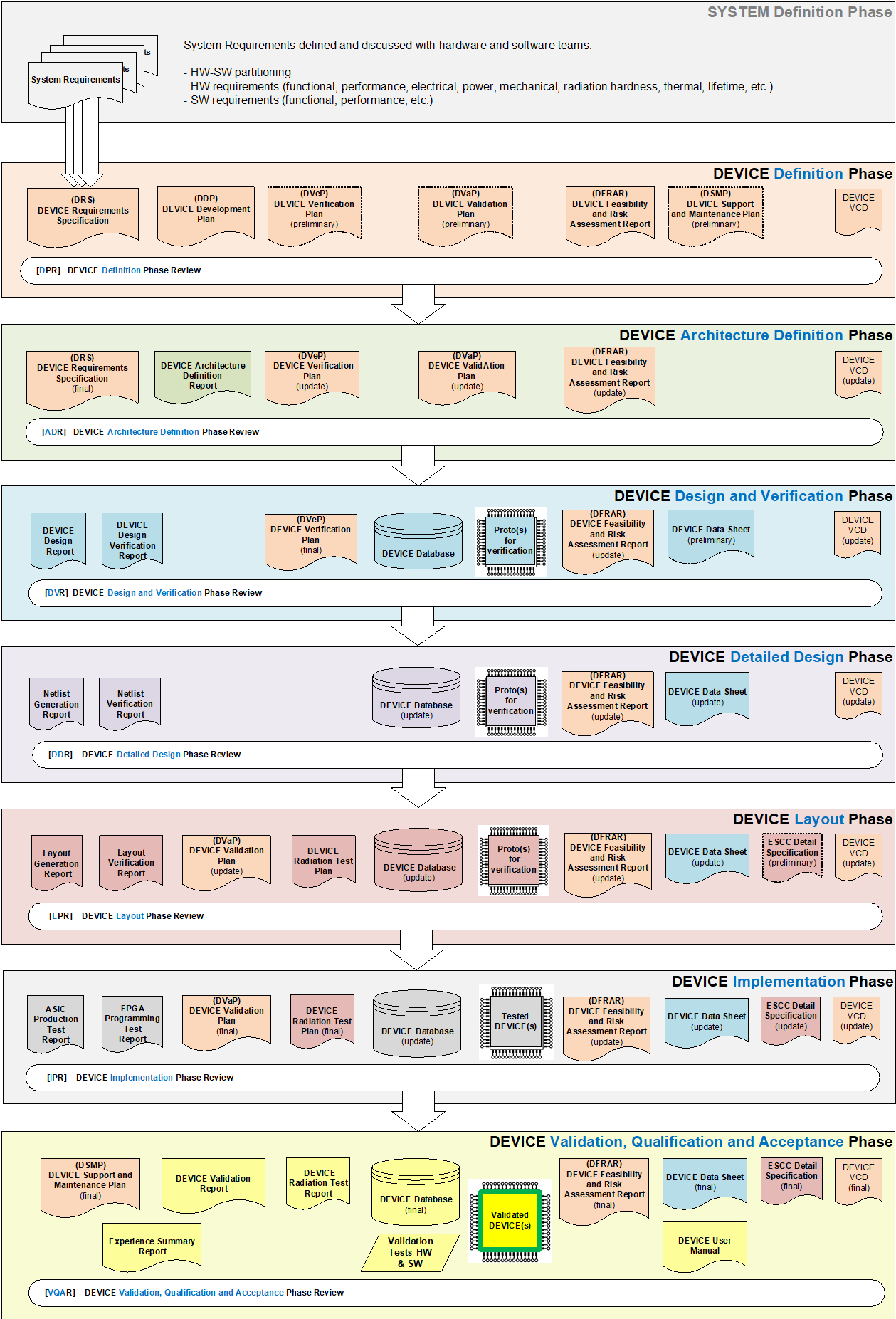 Figure 51: DEVICE development flow (generic case)
DEVICE Definition Phase
Overview
The aim of this initial DEVICE Definition Phase is to establish a DEVICE Development Plan that defines the development flow, indicating the resources and schedules, a DEVICE Requirements Specification that results from carefully flowing down the requirements of the system(s) where the DEVICE is used and ensuring good traceability between the DEVICE requirements and the System Requirements. In addition, a Feasibility and Risk Assessment of the DEVICE development is an important part of this initial DEVICE Definition Phase and is revised in the following phases in order to minimise risks.
DEVICE Requirements Specification
ECSS-E-ST-20-40_1580019The supplier shall specify the complete set of DEVICE requirements in the DEVICE Requirements Specification in compliance with DRD from Annex A. [ALL]
ECSS-E-ST-20-40_1580020The supplier shall ensure that all System Requirements that are relevant to the DEVICE are flowed down to the DRS allowing back traceability. [ALL]
ECSS-E-ST-20-40_1580021If the DEVICE contains one or more processing unit, the supplier shall flow the HW-SW partitioning requirements in the System Requirements down into the DEVICE Requirements Specification. [D-ASIC, --, FPGA, IP]
HW-SW partitioning is usually done by the System team, often the customer, in collaboration with HW and SW development teams (see requirement 5.2.2.4.a of ECSS-E-ST-40).
DEVICE Development Plan
ECSS-E-ST-20-40_1580022The supplier shall provide the customer with a complete description of the DEVICE development global strategy in the DEVICE Development Plan which in compliance with DRD from Annex B. [ALL]
ECSS-E-ST-20-40_1580023The development methodology of any subcontractors in charge of developing any of the Building Blocks for the DEVICE shall be ascertained by the supplier and agreed with the customer. [ALL]
For example, whether deviations or tailoring to ECSS-E-ST-20-40 are applied.
ECSS-E-ST-20-40_1580024Design and verification responsibilities shall be assigned to different people in order to guarantee independent verification. [ALL]
For example, the FPGA Responsible Engineer can take over the role of the FPGA Designer or of the FPGA Verification Engineer, but not both.
ECSS-E-ST-20-40_1580025If the DEVICE contains one or more processing units, the supplier shall plan and document how to synchronise the DEVICE development flow key milestones with the System and SW development flows key milestones in order to manage dependencies between DEVICE, SW and System developments. [D-ASIC, --, FPGA, IP]
ECSS-E-ST-20-40_1580026If the DEVICE contains both analogue and digital blocks, the supplier shall plan and document how to synchronise the DEVICE development flow key milestones with the analogue and digital development flows key milestones in order to manage dependencies. [ALL]
ECSS-E-ST-20-40_1580027Modifications to IP Cores shall be justified and agreed between supplier and customer, documented in the DDP, DVeP and DVaP, specified in DRDs of Annex B, Annex C, and Annex D, and updated accordingly whenever these modifications are agreed. [ALL]
Preliminary Verification and Validation Plans
ECSS-E-ST-20-40_1580028The supplier shall define the general approach to verifying and validating the DEVICE in preliminary Verification and Validation Plans in compliance with DRDs from Annex C and Annex D. [ALL]
ECSS-E-ST-20-40_1580029The supplier shall include the different types of verification and validation methods and test procedures, and a preliminary matrix for the traceability. [ALL]
For example, which parts of the DEVICE are verified and validated separately, whether or not preliminary HW prototypes are used for DEVICE verification, specific Design-for-Test and test modes needed to accelerate otherwise too lengthy verification or validation steps, verification and validation approach when processing units are part of the DEVICE.
ECSS-E-ST-20-40_1580030Modified IP Cores shall be treated as Building Blocks that undergo full verification and validation. [ALL]
Preliminary DEVICE Support and Maintenance Plan
ECSS-E-ST-20-40_1580031If agreed between supplier and customer a preliminary DEVICE Support and Maintenance Plan shall be produced by the supplier in compliance with DRD from Annex E. [ALL]
Feasibility and Risk Assessment
ECSS-E-ST-20-40_1580032The supplier shall perform a feasibility and risk assessment of the development of the DEVICE and document it in the DEVICE Feasibility and Risk Assessment Report in compliance with DRD in Annex F. [ALL]
DEVICE Definition Phase Review
ECSS-E-ST-20-40_1580033The DEVICE Definition Phase shall be concluded by a DEVICE Definition Phase Review in compliance with requirements from clause 5.1.4. [ALL]
ECSS-E-ST-20-40_1580034The reviewers shall check that the DEVICE development activity as defined in the DDP as in DRD in Annex B is feasible within the limits imposed by the project requirements, resources, schedule and budgetary constraints. [ALL]
ECSS-E-ST-20-40_1580035The following expected outputs shall be reviewed during DEVICE Definition Phase Review: [ALL]
- DEVICE Requirements Specification (DRS) as in DRD in Annex A
- DEVICE Development Plan (DDP) as in DRD in Annex B
- DEVICE Verification Plan (preliminary) as in DRD in Annex C
- DEVICE Validation Plan (preliminary) as in DRD in Annex D
- DEVICE Support and Maintenance Plan (preliminary) as in DRD in Annex E
- DEVICE Feasibility and Risk Assessment Report (DFRAR) as in DRD in Annex F
- DEVICE VCD (preliminary)
DEVICE Architecture Definition Phase
Overview
The aim of this development phase is to define the architecture of the DEVICE design in terms of its main functional blocks, hierarchies and dependencies of these blocks, their interfaces and how they interconnect. The objective is to facilitate the modular and detailed design of all the blocks and their integration in the following phases.
Architecture Definition
ECSS-E-ST-20-40_1580036The supplier shall define the DEVICE architecture and document it in the DEVICE Architecture Definition Report in compliance with DRD in Annex G. [ALL]
ECSS-E-ST-20-40_1580037Any pertinent additions and modifications to the DRS of DRD in Annex A due to the DEVICE architecture definitions shall be included in a final DRS. [ALL]
This is done in order to guide the DEVICE designers’ work in the lower-level DEVICE Design and Verification Phase and later in the DEVICE Detailed Design Phase.
Updated DEVICE Verification and Validation Plans
ECSS-E-ST-20-40_1580038The supplier shall update and maintain the preliminary DEVICE Verification and Validation Plans in accordance with Annex C and Annex D, defining verification methods and validation test procedures for requirements impacting the DEVICE architecture definition. [ALL]
For example, test procedures to validate radiation effects mitigation techniques introduced at DEVICE architectural level or HW-SW interfaces and functional dependencies.
DEVICE Architecture Definition Phase Review
ECSS-E-ST-20-40_1580039The DEVICE Architecture Definition Phase shall be concluded by a DEVICE Architecture Definition Phase Review in compliance with requirements from clause 5.1.4. [ALL]
ECSS-E-ST-20-40_1580040The reviewers shall check that the selected architectural trade-offs meet the requirements fixed during the DEVICE Definition Phase. [ALL]
ECSS-E-ST-20-40_1580041The following expected outputs shall be reviewed during DEVICE Architecture Definition Phase Review: [ALL]
- DEVICE Architecture Definition Report as in DRD in Annex G
- DEVICE Requirements Specification (final) as in DRD in Annex A.
- DEVICE Verification plan (update) (DVeP) as in DRD in Annex C
- DEVICE Validation Plan (update) (DVaP) as in DRD in Annex D
- DEVICE Feasibility and Risk Assessment Report (update) (DFRAR) as in DRD in Annex F
- DEVICE VCD (update)
DEVICE Design and Verification Phase
Overview
The aim of the DEVICE Design and Verification Phase is to further develop the DEVICE creating the first DEVICE models and their verification environment. These models are part of the DEVICE Database. The DEVICE model creation and its verification is documented in the DEVICE Design Report and the DEVICE Design Verification Report respectively, a preliminary DEVICE Data Sheet is prepared, and the phase concludes with the DEVICE Design and Verification Phase Review securing that everything is ready for the DEVICE Detailed Design Phase.
DEVICE Verification Plan
ECSS-E-ST-20-40_1580042A DEVICE Verification Plan in compliance with DRD in Annex C shall be completed and ready at DEVICE Design and Verification Phase Review. [ALL]
DEVICE Design and Verification
ECSS-E-ST-20-40_1580043Tasks specified in requirements 5.4.3b to 5.4.3j shall be performed and documented by the supplier in a DEVICE Design Report. [ALL]
ECSS-E-ST-20-40_1580044The supplier shall generate the DEVICE models needed as input to the subsequent DEVICE Detailed Design Phase. [ALL]
- 1 For example, synthesizable RTL models for digital circuits, or behavioral models for analogue circuits.
- 2 Simulations of DEVICE behavioral models of critical functions and algorithms can be very useful during the DEVICE Architecture Definition Phase and Feasibility and Risk Assessment, as they can be valuable tools for further verification tasks.
ECSS-E-ST-20-40_1580045The supplier shall model analogue block interfaces, drivers and loads including their estimated parasitics. [--, A-ASIC, --, --]
For example, parasitics introduced by the package, bonding or wiring tracks.
ECSS-E-ST-20-40_1580046The supplier shall perform an analysis of key analogue parameters and their sensitivity to manufacturing and environmental variations in order to consequently protect the DEVICE analogue blocks against those variations. [--, A-ASIC, --, --]
For example, parameters such as circuit dimensions or electrical parameters which can be affected by process manufacturing and external T, V or I variations.
ECSS-E-ST-20-40_1580047The supplier shall define and document the global approach to integration of new and existing Building Blocks and IP Cores up until the entire DEVICE is integrated at top level. [ALL]
ECSS-E-ST-20-40_1580048The supplier shall generate the necessary DEVICE verification files, verify the DEVICE models following the DEVICE Verification Plan of DRD in Annex C and document results in the first iteration of the DEVICE Design Verification Report. [ALL]
Verification files examples are HDL simulation testbenches, external components models, and data files defining stimuli and expected outputs.
ECSS-E-ST-20-40_1580049The supplier shall perform a preliminary floorplan and a preliminary technology mapping to ensure a successful place-and-route and timing closure in cases where this early assessment can be of added value. [D-ASIC, A-ASIC, FPGA,--]
Technology mapping for digital circuits can be achieved for example by synthesis tools that transform RTL models into gate-level netlists.
ECSS-E-ST-20-40_1580050The supplier shall re-assess the feasibility and risks, including trade-offs for any conflicting requirements, update the DFRAR and implement the best design choices accordingly. [ALL]
For example, power consumption versus speed and performance, pin count versus package size and complexity versus die area, update the DFRAR and implement the best design choices accordingly.
ECSS-E-ST-20-40_1580051The supplier shall specify the configuration applied to IP Cores used in the DEVICE. [ALL]
ECSS-E-ST-20-40_1580052The supplier shall specify any modifications done to IP Cores as justified in the DFRAR and agreed between supplier and customer. [ALL]
ECSS-E-ST-20-40_1580053The radiation hardening approach shall be implemented and verified at this development level. [ALL]
For example, TMR, safe state machines or error detection and correction at RTL HDL level.
DEVICE Database
ECSS-E-ST-20-40_1580054The supplier shall create and maintain a DEVICE Database with all the files needed as inputs for the DEVICE Detailed Design Phase and phase reiterations, including items specified in 5.4.4b to 5.4.4d. [ALL]
ECSS-E-ST-20-40_1580055The DEVICE Database shall include the DEVICE models and other electronic files needed for the complete DEVICE netlist generation. [ALL]
For example, high-level simulation, behavioral and RTL models and analogue design models.
ECSS-E-ST-20-40_1580056The DEVICE Database shall include the executable and script files used for verification of the DEVICE models. [ALL]
For example, testbenches, simulation control or constraint files, external component models, stimuli input files and expected output files, ad-hoc executable files to process verification results and results log files.
ECSS-E-ST-20-40_1580057The DEVICE Database shall include the description of what the DEVICE Database contains, including the files’ structure, naming conventions and version control labels. [ALL]
Preliminary DEVICE Data Sheet
ECSS-E-ST-20-40_1580058If agreed with the customer, the supplier shall generate a preliminary DEVICE Data Sheet in compliance with DRD from Annex H. [ALL]
- 1 Data Sheets are in general intended for users of the DEVICE who do not have access to the DEVICE development documents such as the DEVICE Requirements Specification.
- 2 For example, if the DEVICE is marketed as an off-the-shelf product.
- 3 Some of the DEVICE technical parameters are inherent to the technology used to implement the DEVICE and therefore can be provided by the technology provider for example in the form of blank FPGA Data Sheets or ASIC manufacturer and standard cell library documents.
ECSS-E-ST-20-40_1580059The preliminary DEVICE Data Sheet shall contain all parts of the final DEVICE Data Sheet, with the same level of detail, using clearly identified estimated values for those parameter values that are not yet confirmed. [ALL]
For example, preliminary values can be obtained by simulation or measurements on a prototype, while final parameter values are confirmed with the validated DEVICE.
ECSS-E-ST-20-40_1580060The preliminary DEVICE Data Sheet shall contain at least the main functionalities and interfaces of the DEVICE. [ALL]
This information can be provided in the form of Interface Control Document (ICD) as defined in ECSS-E-ST-40 Annex E.
DEVICE Design and Verification Phase Review
ECSS-E-ST-20-40_1580061The DEVICE Design and Verification Phase shall be concluded by the DEVICE Design and Verification Phase Review in compliance with requirements from clause 5.1.4. [ALL]
ECSS-E-ST-20-40_1580062The following expected outputs shall be reviewed during DEVICE Design and Verification Phase Review: [ALL]
- DEVICE Verification Plan (final) (DVeP) as in DRD in Annex C
- DEVICE Design Report
- DEVICE Design Verification Report
- DEVICE Data Sheet (preliminary) as in DRD in Annex H
- DEVICE database
- DEVICE Feasibility and Risk Assessment Report (update) (DFRAR) as in DRD in Annex F
- DEVICE VCD (update)
DEVICE Detailed Design Phase
Overview
During the DEVICE Detailed Design Phase, the DEVICE design is translated into a structural description at the level of elementary cells of the selected technology and cell library: the pre-layout netlist.
Additional information is generated for the subsequent development phases, such as layout constraints, floorplanning, Production Tests programs and a detailed pin description.
For digital designs, the above-mentioned design description is the technology specific gate-level pre-layout netlist normally obtained by synthesis tools.
For analogue designs, it is a verified sized transistor-level netlist. However, in many analogue designs, there is no separation between circuit netlist design and layout.
Meeting DEVICE timing, occupancy and power targets sometimes can need performing iterations between netlist generation and layout generation.
Netlist Generation
ECSS-E-ST-20-40_1580063Tasks specified in requirements 5.5.2b to 5.5.2u shall be performed and documented by the supplier in a Netlist Generation Report. [ALL]
ECSS-E-ST-20-40_1580064The supplier shall confirm use of design tools version as specified in the DEVICE Development Plan of DRD in Annex B, including the tools maintenance status, known bugs and existing patches. [ALL]
ECSS-E-ST-20-40_1580065The supplier shall choose and implement the pre-layout netlist generation with the selected tool options and constraints. [ALL]
For example, script variables and commands to control the timing, area, power, types of library cells used or different synthesis modes for complex DEVICEs.
ECSS-E-ST-20-40_1580066Clock, reset or other signals needing specific generation, buffering and delay-controlled distribution with high fan-out shall be implemented using available netlist generation resources. [D-ASIC, A-ASIC, FPGA, --]
These buffers and signal distribution trees can be implemented during the Layout Phase also, depending on what is the target implementation technology.
ECSS-E-ST-20-40_1580067DFT and Production Tests requirements shall be implemented. [ALL]
ECSS-E-ST-20-40_1580068The radiation hardening approach shall be implemented and verified at netlist level. [ALL]
For example, TMR, safe state machines or error detection and correction generated by netlist synthesis tools.
ECSS-E-ST-20-40_1580069A floorplan shall be defined or refined if already existing. [ALL]
ECSS-E-ST-20-40_1580070I/O buffers and interfaces shall be confirmed and implemented. [ALL]
For example, HSSL, LVDS, tri-state buffers, etc.
ECSS-E-ST-20-40_1580071The supplier shall implement design parameter centring based on simulations, allowing margins that account for final layout and process variations, in order to maximise yield. [--, A-ASIC, --, IP]
ECSS-E-ST-20-40_1580072The supplier shall justify and document any library cells selections. [D-ASIC, A-ASIC, --, IP]
For example, some cells can be excluded from being used due to their weaker radiation performance, or some specific cells get higher priority in being used due to their more favorable timing characteristics.
ECSS-E-ST-20-40_1580073The supplier shall describe any logic cells that were specially developed for the DEVICE. [D-ASIC, A-ASIC, --, IP]
For example, to achieve higher radiation tolerance, to meet testability, manufacturability or power consumption DRS requirements, or to meet technology provider constraints.
ECSS-E-ST-20-40_1580074The supplier shall describe any Design-For-Manufacturability strategies applied during netlist generation. [D-ASIC, A-ASIC, --, --]
ECSS-E-ST-20-40_1580075The supplier shall specify and justify the use of any black-boxes in the netlist. [ALL]
For example, elements of the netlist that cannot be modified by using specific synthesis tool attributes or that cannot be interpreted by synthesis tool, or netlist blocks which are added at a later stage.
ECSS-E-ST-20-40_1580076The supplier shall document all settings applied during netlist generation, including those related to technology supplier or manufacturer-specific design rules. [ALL]
For example, timing, area or power constraints, process variations, temperature and voltage operating conditions, radiation environment constraints and IP Core synthesis constraints provided by the IP provider.
ECSS-E-ST-20-40_1580077Level of utilization of available resources shall be determined and documented. [ALL]
For example, the number of logic and memory cells used, and number of clock and reset dedicated buffers.
ECSS-E-ST-20-40_1580078The supplier shall specify the configuration and netlist generation constraints applied to IP Cores used in the DEVICE netlist. [ALL]
ECSS-E-ST-20-40_1580079Any deviations from IP Core provider recommendations for the netlist generation of the IP Core shall be documented and justified. [ALL]
ECSS-E-ST-20-40_1580080The supplier shall document any applied derating factors. [ALL]
For example, derating factors for timing, current density or power.
ECSS-E-ST-20-40_1580081The supplier shall document any applied margins. [ALL]
For example, margins for timing, area, number of I/Os, LUT or memory blocks.
ECSS-E-ST-20-40_1580082Influences from layout such as cross talk and matching shall be accounted for during the detail design work. [D-ASIC, A-ASIC, --, IP]
ECSS-E-ST-20-40_1580083The supplier shall document how parasitic effects are dealt with. [D-ASIC, A-ASIC, --, IP]
Netlist verification
ECSS-E-ST-20-40_1580084Tasks specified in requirements 5.5.3b to 5.5.3c shall be performed and documented by the supplier in a Netlist Verification Report. [ALL]
ECSS-E-ST-20-40_1580085Verification of the netlist shall be performed in compliance to the DEVICE Verification Plan of DRD in Annex C. [ALL]
ECSS-E-ST-20-40_1580086If Production Tests and functional test modes are planned, the supplier shall generate preliminary test vectors and verify the related DEVICE requirements. [ALL]
DEVICE Data Sheet update
ECSS-E-ST-20-40_1580087The supplier shall update the preliminary DEVICE Data Sheet of DRD in Annex H according to the results obtained during the DEVICE Detailed Design Phase. [ALL]
For example, new information about timing, power consumption, pin-out and resources occupation parameters.
DEVICE Database update
ECSS-E-ST-20-40_1580088The supplier shall update the DEVICE Database with the input files needed for the following DEVICE Layout and Implementation phases, including items specified in 5.5.5b to 5.5.5f. [ALL]
ECSS-E-ST-20-40_1580089The DEVICE Database shall include the pre-layout netlist. [ALL]
ECSS-E-ST-20-40_1580090The DEVICE Database shall include the preliminary set of constraints for layout. [ALL]
For example, a DEVICE floorplan, or timing, power and area constraints. [ALL]
ECSS-E-ST-20-40_1580091The DEVICE Database shall include the preliminary test vectors for Production Tests. [D-ASIC, A-ASIC, --, --]
ECSS-E-ST-20-40_1580092The DEVICE Database shall include the scripts used for an automatic and repeatable generation of the netlist and its verification, and the corresponding result log files. [D-ASIC, A-ASIC, FPGA, --]
ECSS-E-ST-20-40_1580093DEVICE Database description of files structure, naming conventions, and version control labels shall be updated to reflect all the changes. [ALL]
DEVICE Detailed Design Phase Review
ECSS-E-ST-20-40_1580094The DEVICE Detailed Design Phase shall be concluded by the DEVICE Detailed Design Phase Review in compliance with requirements from clause 5.1.4. [ALL]
ECSS-E-ST-20-40_1580095The reviewers shall confirm the complete list of items with name and format to be provided to the company developing the DEVICE layout and manufacturing. [D-ASIC, A-ASIC, --, -- ]
For example, pre-layout netlist files, stimuli files for Production Tests and constraints files.
ECSS-E-ST-20-40_1580096The following expected outputs shall be reviewed during DEVICE Detailed Design Phase Review: [ALL]
- Netlist Generation Report
- Netlist Verification Report
- DEVICE Data Sheet (update) as in DRD in Annex H
- DEVICE Database (update)
- DEVICE VCD (update)
- DEVICE Feasibility and Risk Assessment Report (update) (DFRAR) as in DRD in Annex F
DEVICE Layout Phase
Overview
The aim of the DEVICE Layout Phase is to generate a structural description of the DEVICE at the level of elementary cells of the selected technology and libraries creating a placed and routed model of the netlist and all the complementary files that are needed to manufacture or program the DEVICE.
Layout generation
ECSS-E-ST-20-40_1580097Tasks specified in requirements 5.6.2b to 5.6.2p shall be performed and documented by the supplier in a Layout Generation Report. [ALL]
ECSS-E-ST-20-40_1580098Floorplan of the DEVICE shall be finalised. [D-ASIC, A-ASIC, FPGA, --]
ECSS-E-ST-20-40_1580099The core and I/O-pad power distribution shall be generated. [D-ASIC, A-ASIC, --, --]
ECSS-E-ST-20-40_1580100Test pads, if needed, shall be generated. [D-ASIC, A-ASIC, --, --]
ECSS-E-ST-20-40_1580101The bonding diagram respecting bonding and package constraints shall be generated. [D-ASIC, A-ASIC, --, --]
ECSS-E-ST-20-40_1580102ESD protection circuits shall be generated. [D-ASIC, A-ASIC, --, --]
ECSS-E-ST-20-40_1580103The clock distribution, including clock tree and buffers shall be generated. [D-ASIC, --, --, --]
ECSS-E-ST-20-40_1580104Any other global networks that need place and route decisions shall be generated. [D-ASIC, --, --, --]
For example, reset networks.
ECSS-E-ST-20-40_1580105Final set of constraints and options for the layout generation shall be selected. [D-ASIC, --, FPGA, --]
For example, timing and physical resources.
ECSS-E-ST-20-40_1580106Place and route shall be performed applying all layout constraints. [D-ASIC, --, FPGA, --]
For example, timing and physical resources constraints.
ECSS-E-ST-20-40_1580107Final resources utilization shall be determined. [ALL]
For example, die size, number of logic elements, pre-diffused signal and power networks, in case of FPGAs, and number of I/Os.
ECSS-E-ST-20-40_1580108The supplier shall describe any Design-For-Manufacturability strategies applied during layout generation. [D-ASIC, A-ASIC, --, --]
ECSS-E-ST-20-40_1580109The radiation hardening approach shall be implemented and verified at layout level. [ALL]
For example, laying out asynchronous signal paths with filtering buffers or shaping the topology, widths and lengths of active areas of critical cells and the distances between them.
ECSS-E-ST-20-40_1580110The final ASIC post-layout netlist shall be generated applying manufacturer constraints and design rules and the new timing data extracted from the layout. [D-ASIC, --, --, --]
For example, the pre-layout netlist can be optimized by local re-synthesis or physical or topography synthesis in order to obtain the final post-layout netlist.
ECSS-E-ST-20-40_1580111The final FPGA place and route database files needed for the verification of the FPGA layout shall be generated. [--, --, FPGA, --]
For example, timing files such as SDF used for netlist timing simulation or static timing analysis, pin out assignment reports or power consumption reports.
ECSS-E-ST-20-40_1580112Input files needed for the generation of the ASIC masks or for the FPGA programming shall be generated. [D-ASIC, A-ASIC, FPGA, --]
For example, GDSII files for ASICs or programming bit stream files for FPGAs.
Layout verification
ECSS-E-ST-20-40_1580113The supplier shall perform comprehensive layout and post-layout or post-place-and-route netlist verification according to the DEVICE Verification Plan specified in DRD in Annex C and document the results in the Layout Verification Report. [D-ASIC, A-ASIC, FPGA, --]
ECSS-E-ST-20-40_1580114Major warnings and deviations from technology provider rules found during verification shall be analysed and reported in the Layout Verification Report. [D-ASIC, A-ASIC, FPGA, --]
DEVICE Validation Plan
ECSS-E-ST-20-40_1580115The supplier shall complete and consolidate the final DEVICE Validation Plan detailing all the validation test procedures to be carried out and in compliance with DRD in Annex D. [ALL]
ECSS-E-ST-20-40_1580116If agreed with the customer, radiation test procedures shall be defined and documented in a dedicated DEVICE Radiation Test Plan. [ALL]
DEVICE Database update
ECSS-E-ST-20-40_1580117Files generated during DEVICE Detailed Design Phase shall be added to the DEVICE Database. [D-ASIC, A-ASIC, FPGA, --]
For example, post-layout netlist, SDF files, FPGA bit stream files and ASIC GDSII files.
ECSS-E-ST-20-40_1580118The DEVICE Database shall include the scripts used for an automatic and repeatable generation of the layout files and their verification, and the corresponding result log files. [D-ASIC, A-ASIC, FPGA, --]
ECSS-E-ST-20-40_1580119The DEVICE Database description of files structure, naming conventions, version control labels shall be updated to reflect all the changes. [D-ASIC, A-ASIC, FPGA, --]
DEVICE Data Sheet update
ECSS-E-ST-20-40_1580120The supplier shall update the parameters in the DEVICE Data Sheet of DRD in Annex H according to the results obtained during the layout verification. [ALL]
For further details see Annex H.
Preliminary ESCC Detail Specification
ECSS-E-ST-20-40_1580121If agreed between supplier and customer, a preliminary ESCC Detail Specification shall be established in conformance with the ESCC system and based in the DEVICE information gathered so far and until DEVICE Layout Phase. [D-ASIC, A-ASIC, FPGA, --]
- 1 ESCC Detail Specification is usually needed when the DEVICE undergoes ESCC procurement, evaluation or qualification.
- 2 The final ESCC Detail Specification is consolidated later with additional information acquired during the DEVICE Validation Phase.
DEVICE Layout Phase Review
ECSS-E-ST-20-40_1580122The DEVICE Layout Phase shall be concluded by the DEVICE Layout Phase Review in compliance with requirements from clause 5.1.4. [ALL]
ECSS-E-ST-20-40_1580123The reviewers shall check that any outputs of previous phases that have not been reviewed yet are reviewed and confirmed as ready for the final physical implementation of the DEVICE. [ALL]
For example, if the DEVICE Detailed Design Phase Review was skipped and merged with the DEVICE Layout Phase Review.
ECSS-E-ST-20-40_1580124The following expected outputs shall be reviewed during DEVICE Layout Phase Review: [ALL]
- Layout Generation Report
- Layout Verification Report
- DEVICE Validation Plan (update) (DVaP) as in DRD in Annex D
- DEVICE Radiation Test Plan
- DEVICE Data Sheet (update) as in DRD in Annex H
- ESCC Detail Specification (preliminary)
- DEVICE database (update)
- DEVICE VCD (update)
- DEVICE Feasibility and Risk Assessment Report (update) (DFRAR) as in DRD in Annex F
DEVICE Implementation Phase
Overview
In the DEVICE Implementation Phase the final ASIC DEVICE is manufactured, packaged and prototypes go through Production Tests, the final FPGA DEVICE is programmed, or the final IP Core is implemented in a selected technology, in compliance with DEVICE Development Plan. The phase concludes by the delivery of the tested DEVICEs which undergo validation and customer acceptance in the DEVICE Validation, Qualification and Acceptance Phase, and with the DEVICE Implementation Phase Review.
Production and test
ECSS-E-ST-20-40_1580125Tasks specified in requirements 5.7.2b to 5.7.2e shall be performed and documented by the supplier in an ASIC Production Tests Report, for ASICs, and an FPGA Programming Test Report for FPGAs. [D-ASIC, A-ASIC, FPGA, --]
ECSS-E-ST-20-40_1580126The committed number of DEVICEs using the technology choices specified in the DEVICE Development Plan of DRD in Annex B and DEVICE Requirements Specification of DRD in Annex A shall be manufactured, for ASIC, or programmed, for FPGA. [D-ASIC, A-ASIC, FPGA, --]
ECSS-E-ST-20-40_1580127ASIC Production Tests shall be performed on the ASIC batch agreed between customer and supplier used for the validation tests during the DEVICE Validation, Qualification and Acceptance Phase in compliance with DEVICE Validation Plan specified in the DRD of Annex D. [D-ASIC, A-ASIC, --, --]
ECSS-E-ST-20-40_1580128FPGA Programming Test shall be performed on the same devices used for the validation tests during the DEVICE Validation, Qualification and Acceptance Phase. in compliance with DEVICE Validation Plan as per DRD Annex D. [--, --, FPGA, --]
ECSS-E-ST-20-40_1580129The supplier shall generate the FPGA Programming Test Report including the following: [--, --, FPGA, --]
- FPGA programming steps indicating compliance to the FPGA technology provider's "FPGA programming guidelines".
- Input and output files, specifying the format, identifier, version of netlist files, checksum and bit stream files used and generated during programming.
- HW and SW equipment used.
- The exact FPGA device part used, including serial number and date code.
DEVICE Database update
ECSS-E-ST-20-40_1580130Files generated during the DEVICE Implementation Phase shall be added to the DEVICE Database. [D-ASIC, A-ASIC, FPGA, --]
- 1 For example, new FPGA bit stream files for the final FPGA technology.
- 2 Expected outputs of the DEVICE Implementation phase are the ASIC Production Tests Report or FPGA Programming Test Report, all files used during the production or programming tests and the agreed number of tested DEVICEs.
DEVICE Validation Plan completion
ECSS-E-ST-20-40_1580131The final DEVICE Validation Plan shall be completed as per Annex D in order to start the DEVICE validation test procedures in the following phase. [ALL]
DEVICE Implementation Phase Review
ECSS-E-ST-20-40_1580132The DEVICE Implementation Phase shall be concluded by the DEVICE Implementation Phase Review in compliance with requirements from clause 5.1.4. [ALL]
ECSS-E-ST-20-40_1580133The following expected outputs shall be reviewed during DEVICE Implementation Phase Review: [ALL]
- DEVICE Validation Plan (final) (DVaP) as in DRD in Annex D
- DEVICE Radiation Test Plan (final)
- ASIC Production Tests Report or
- FPGA Programming Tests Report
- DEVICE Data Sheet (update) as in DRD in Annex H
- ESCC Detail Specification (update)
- DEVICE database (update)
- DEVICE VCD (update)
- DEVICE Feasibility and Risk Assessment Report (update) (DFRAR) as in DRD in Annex F
- Agreed number of tested DEVICEs
DEVICE Validation, Qualification and Acceptance Phase
Overview
This is the last phase of the development of the DEVICE. The manufactured or programmed parts which already went through Production Tests, in case of ASICs, or Programming Test, in case of FPGAs, now undergo validation test procedures, as defined in the DEVICE Validation Plan, and if agreed with the customer, radiation tests too. Sometimes these validation tests help to uncover problems or defects in the DEVICE technology provided by the ASIC manufacturer or the DEVICE technology provider. Sometimes the validation tests find design problems that were unfortunately not detected by verification due to tools or design kits limitations or not exhaustive verification coverage. With the data measured in all these tests, the existing versions of the DEVICE user and procurement documents, as agreed with the customer, are corrected and completed by the supplier. The DEVICE Validation, Qualification and Acceptance Phase Review, once declared successful, constitutes the acceptance by the customer of the outputs contractually agreed as deliverables.
In some cases, contractually agreed deliverables can include some of the expected output hardware such as validation tests boards, and software used for the validation test procedures.
DEVICE validation
ECSS-E-ST-20-40_1580134Tasks specified in requirements 5.8.2b to 5.8.2f shall be performed and documented by the supplier in the DEVICE Validation Report. [ALL]
ECSS-E-ST-20-40_1580135The DEVICE validation test procedures shall be performed in compliance with the DEVICE Validation Plan specified in DRD Annex D. [ALL]
ECSS-E-ST-20-40_1580136The supplier shall design and build the validation tests set-up representative of the intended system application environment as defined in the DEVICE Validation Plan. [ALL]
ECSS-E-ST-20-40_1580137The supplier shall use the validation tests set-up to perform validation test procedures that cover all requirements in compliance with DEVICE Validation Plan. [ALL]
Requirements validated include functional, electrical, environmental, test modes and stress conditions.
ECSS-E-ST-20-40_1580138If agreed with the customer and planned in the DEVICE Validation Plan, the supplier shall perform ESCC evaluation or qualification tests. [D-ASIC, A-ASIC, FPGA, --]
For example, as defined in ESCC 9000 specifications: burn-in, V/T stress tests or screening tests.
ECSS-E-ST-20-40_1580139If agreed with the customer and according to the DEVICE Radiation Test Plan, the supplier shall perform radiation test procedures and document the results in the DEVICE Radiation Test Report. [ALL]
DEVICE Support and Maintenance
ECSS-E-ST-20-40_1580140The final DEVICE Support and Maintenance Plan shall be agreed with the customer and produced by the supplier in compliance to DRD in Annex E. [ALL]
ECSS-E-ST-20-40_1580141Any support and maintenance activities done during this phase shall be logged in predefined formats and retained in maintenance records. [ALL]
Experience Summary Report
ECSS-E-ST-20-40_1580142If agreed with the customer, an Experience Summary Report shall be generated in compliance with DRD in Annex I. [ALL]
Final versions of application and procurement documents
ECSS-E-ST-20-40_1580143If agreed with the customer, the final ESCC Detail Specification shall be updated based on the validation test results. [D-ASIC, A-ASIC, FPGA, --]
ECSS-E-ST-20-40_1580144For DEVICEs that are used as off-the-shelf products the final DEVICE Data Sheet shall be updated based on the validation test results. [ALL]
ECSS-E-ST-20-40_1580145If agreed with the customer, a DEVICE User Manual document shall be established in order to guide DEVICE users through different electrical and functional configurations of the DEVICE in typical system applications. [ALL]
For example, describing suitable bias circuitry, supply voltages and configuration modes for typical use scenarios.
DEVICE Validation, Qualification and Acceptance Phase Review
ECSS-E-ST-20-40_1580146The DEVICE Validation, Qualification and Acceptance Phase shall be concluded by the DEVICE Validation, Qualification and Acceptance Phase Review in compliance with requirements from clause 5.1.4. [ALL]
ECSS-E-ST-20-40_1580147The reviewers shall review expected outputs of DEVICE Implementation Phase, in addition to all the expected outputs of this DEVICE Validation, Qualification and Acceptance Phase. [ALL]
ECSS-E-ST-20-40_1580148The reviewers shall check that the DEVICE meets all functional, performance, interface and other requirements in compliance with the DEVICE Requirements Specification as per DRD Annex A. [ALL]
ECSS-E-ST-20-40_1580149The reviewers shall check that preventive measures or contingency plans exist for all identified risk items reported in the DFRAR, including any new ones identified in the Validation, Qualification and Acceptance Phase, in order to accept the identified risks prior to: [ALL]
- DEVICE acceptance by the customer
- FM production, if planned. ECSS-E-ST-20-40_1580150The following expected outputs shall be reviewed during DEVICE Validation, Qualification and Acceptance Phase Review: [ALL]
- Agreed number of tested and validated DEVICEs
- DEVICE Validation Report
- DEVICE Radiation Test Report
- DEVICE Feasibility and Risk Assessment Report (final) (DFRAR) as in DRD in Annex F
- DEVICE Support and Maintenance Plan (final) (DSMP) as in DRD in Annex E
- Experience Summary Report as in DRD in Annex I
- DEVICE Data Sheet (final) as in DRD in Annex H
- ESCC Detail Specification (final)
- DEVICE User Manual
- Validation Tests hardware and software
- DEVICE Database (final)
- DEVICE VCD (final).
Pre-tailoring according to DEVICE criticality and type
DEVICE criticality categories
Criticality categories are assigned to DEVICE products as specified in ECSS-Q-ST-30 clause 5.4 which specifies the relationship between the criticality category of the DEVICE products, the highest criticality of the functions implemented by the DEVICE and the existing system compensating provisions.
To any DEVICE described in the second right column of Table 61 the corresponding criticality category in the left column is assigned. Dependability and safety consequences associated to each DEVICE criticality as per ECSS-Q-ST-30 Table 5-1 are also indicated in Table 61 below.
Table 61: DEVICE criticality categories
|
DEVICE criticality category
|
Definition
|
Dependability consequences
|
Safety consequences
|
|
A |
DEVICE involved in category I functions
|
Failure propagation (Only for lower than system level analysis) (refer to requirement 5.3.2.c of ECSS-Q-ST-30)
|
Loss of life, life-threatening or permanently disabling injury or occupational illness Loss of system Loss of an interfacing manned flight system Loss of launch site facilities Severe detrimental environmental effects |
|
DEVICE included in compensating provisions for category I functions
| |||
|
B |
DEVICE involved in category I functions
|
Loss of mission
|
Temporarily disabling but not life threatening injury, or temporary occupational illness Major damage to an interfacing flight system Major damage to ground facilities Major damage to public or private property Major detrimental environmental effects |
|
DEVICE involved in category II functions
| |||
|
DEVICE included in compensating provisions for category II functions
| |||
|
C |
DEVICE involved in category II functions
|
Major mission degradation
|
|
|
DEVICE involved in category III functions
| |||
|
DEVICE included in compensating provisions for category III functions
| |||
|
D |
DEVICE involved in category III functions
|
Minor mission degradation or any other effect
|
|
|
DEVICE involved in category IV functions
|
Pre-tailoring Matrix
The following applicability matrix, Table 62, represents a tailoring of the requirements of ECSS-E-ST-20-40 based on the DEVICE type and the DEVICE criticality category defined respectively in previous clause 6.1.
For each requirement of this Standard and for each DEVICE type and criticality category, an indication is given on whether that requirement is applicable (“yes”), not applicable (“no”), or partially applicable as specified for a DEVICE of criticality category D. By default, all requirements are applicable to DEVICEs of criticality categories A, B and C.
The right most column indicates with a “yes” which requirements are conditional requirements, because they are only applicable if the stated condition of the requirement main text is met.
This pre-tailoring matrix is not following the same structure as in ECSS-Q-ST-30 clause 8 where the pre-tailoring is done according to the following space product types such as space system, space segment element, launch segment element, ground segment element and sub-systems, etc.
Table 62: Pre-tailoring Matrix
|
ECSS Source ID |
Requirement main text |
Requirement NOTES |
Digital ASIC |
Analog ASIC |
FPGA |
IP Core |
ifCRITICALITY Category D |
Conditional requirement |
|
5.1 |
General requirements |
|
|
|
|
|
|
|
|
5.1.2 |
Tailoring according to DEVICE type and DEVICE criticality |
|
|
|
|
|
|
|
|
5.1.2a |
Criticality category of the DEVICE under development shall be discussed and agreed with the customer. [ALL] |
|
yes |
yes |
yes |
yes |
yes |
|
|
5.1.2b |
Customer and supplier shall define the final tailoring of the requirements of ECSS-E-ST-20-40 according to the type of DEVICE and according to its criticality category in compliance with clause 6. [ALL] |
|
yes |
yes |
yes |
yes |
yes |
|
|
5.1.3 |
DEVICE engineering development flow |
|
|
|
|
|
|
|
|
5.1.3a |
The DEVICE development phases and milestones shall be in conformance with the generic engineering flow presented in Figure 51. [ALL] |
NOTE 1 The equivalence of ECSS-M-ST-10 phases and milestone names with respect to ECSS-E-ST-20-40 is presented in Annex L.NOTE 2 The most complex expected document outputs are defined in DRD annexes, while the content of other expected documents outputs is defined in the main chapters of the standard, and this information is summarized in Table K-2. |
yes |
yes |
yes |
yes |
yes |
|
|
5.1.3b |
If the DEVICE Development Plan includes any variations with respect to the generic flow shown in Figure 51, all the outputs expected at every new phase and associated review shall reflect these changes too. [ALL] |
NOTE 1 For example, in case of having phase iterations or additional sub-phases and reviews, the Verification and Validation Plans include what requirements are covered in each new phase.NOTE 2 Annex J describes the main types of DEVICE development flow variations. |
yes |
yes |
yes |
yes |
yes |
yes |
|
5.1.3c |
Each planned additional intermediate step, parallel step or not planned design iteration leading to a new DEVICE database release shall undergo its own dedicated review. [ALL] |
|
yes |
yes |
yes |
yes |
no |
|
|
5.1.3d |
If the DEVICE development is planned to undergo a first Engineering Model development followed by a Flight Model development, customer and supplier shall agree whether EM and FM are treated as two independent DEVICE developments or as a single DEVICE development where the EM is mainly a prototype verification step for the development of the final FM DEVICE. [ALL] |
NOTE 1 Treating EM and FM as independent developments can be adequate whenever their respective implementation technologies are significantly different, and therefore the models of EM and FM DEVICEs are significantly different too.NOTE 2 Treating EM and FM as independent developments can also be adequate if EM DEVICE is planned to be used as a stand-alone product and not just as an intermediate verification step for the FM DEVICE. |
yes |
yes |
yes |
yes |
yes |
yes |
|
5.1.3e |
All inputs and tools used to reproduce DEVICE development steps in every phase shall follow the documentation and configuration management requirements in compliance with clause 8 of ECSS-Q-ST-60-03. [ALL] |
NOTE 1 Examples of such inputs are simulation test patterns, schematics, VHDL source codes and synthesis scripts.NOTE 2 Examples of DEVICE development steps are netlist generation and netlist verification.NOTE 3 Tools are any design, verification and validation software and hardware tools used during the DEVICE development. |
yes |
yes |
yes |
yes |
no |
|
|
5.1.3f |
The supplier shall ensure automatic repeatability of all development steps that make use of CAD tools that support automation in order to facilitate iterations in the flow. [ALL] |
NOTE Examples of planned iterations include repetitions of self-checking simulations as the design is maturing. But iterations in the development flow can also be needed due to unexpected changes to the requirements, the technology or any unforeseen modifications to the design |
yes |
yes |
yes |
yes |
no |
|
|
5.1.3g |
In order to reopen a phase that was successfully closed already, supplier and customer shall discuss and reach an agreement on it. [ALL] |
|
yes |
yes |
yes |
yes |
yes |
|
|
5.1.3h |
Every output shall be updated at the end of every phase with any relevant new information gathered during the phase. [ALL] |
|
yes |
yes |
yes |
yes |
yes |
|
|
5.1.4 |
Phase Reviews |
|
|
|
|
|
|
|
|
5.1.4a |
The outputs generated within each phase shall be reviewed by the customer with the support of the supplier. [ALL] |
|
yes |
yes |
yes |
yes |
yes |
|
|
5.1.4b |
The reviewers shall analyse the preventive measures and contingency plans for all identified open issues and risk items identified in the DEVICE Feasibility and Risk Assessment to define and agree with the customer the risks that are taken for starting the next phase. [ALL] |
|
yes |
yes |
yes |
yes |
yes |
|
|
5.1.4c |
The reviewers shall check that all expected outputs contain all the relevant information and with a level of detail that avoids ambiguity. [ALL] |
|
yes |
yes |
yes |
yes |
yes |
|
|
5.1.4d |
Any missing information and open points and their impact on following phases shall be assessed, registered and agreed with the customer in the MoM of the phase review with an indication of the expected time of completion of the open points. [ALL] |
|
yes |
yes |
yes |
yes |
yes |
|
|
5.1.4e |
The criteria for a successful phase review shall be defined in advance. [ALL] |
|
yes |
yes |
yes |
yes |
yes |
|
|
5.1.4f |
Phase reviews shall be conducted in accordance with ECSS-M-ST-10 and ECSS-M-ST-10-01. [ALL] |
|
yes |
yes |
yes |
yes |
no |
|
|
5.1.5 |
DEVICE Verification Control Document |
|
|
|
|
|
|
|
|
5.1.5a |
At DEVICE Definition Phase review the supplier shall provide for customer approval an initial DEVICE VCD, in compliance with ECSS-E-ST-10-02 Annex B VDC DRD, including [ALL]1. the DEVICE requirements with the combination of the selected verification and validation methods for the different verification and validation levels at the applicable development phases and the applicable verification stages.2. The traceability between DEVICE requirements and System requirements in compliance with ECSS-E-ST-10-06 clause 8.2.3. |
NOTE 1 Verification stages can be qualification, acceptance, prelaunch, in-orbit (including commissioning) and postlanding, as defined in ECSS-E-ST-10-02 clause 4.2.4. NOTE 2 Verification methods are defined in ECSS-E-ST-20-40 clause 4.2. NOTE 3 Some verification and validation information can be found in ECSS-E-ST-20-40 reports and used to populate parts of the VCD. These reports are Design Verification Report, Netlist Verification Report, Layout Verification Report, ASIC Production Test Report, FPGA Programming Test Report, DEVICE Validation Report and Radiation Test Report. NOTE 4 References to relevant sections of the DVerP, DValP, or reports, waivers, RFD, NCR, NRB or customer closeout reports can be added to VCD to demonstrate compliance with the requirements. NOTE 5 The DEVICE VCD can be included in the upper level VCD, for example, equipment or unit VCD. |
yes |
yes |
yes |
yes |
yes |
|
|
5.1.5b |
The supplier shall provide for customer approval an updated DEVICE VCD with the verification and validation close out status for the DEVICE at each phase review in compliance with ECSS-E-ST-10-02 Annex B VCD DRD. [ALL] |
|
yes |
yes |
yes |
yes |
yes |
|
|
5.2 |
DEVICE Definition Phase |
|
|
|
|
|
|
|
|
5.2.2 |
DEVICE Requirements Specification |
|
|
|
|
|
|
|
|
5.2.2a |
The supplier shall specify the complete set of DEVICE requirements in the DEVICE Requirements Specification in compliance with DRD from Annex A. [ALL] |
|
yes |
yes |
yes |
yes |
yes |
|
|
5.2.2b |
The supplier shall ensure that all System Requirements that are relevant to the DEVICE are flowed down to the DRS allowing back traceability. [ALL] |
|
yes |
yes |
yes |
yes |
yes |
|
|
5.2.2c |
If the DEVICE contains one or more processing unit, the supplier shall flow the HW-SW partitioning requirements in the System Requirements down into the DEVICE Requirements Specification. [D-ASIC, --, FPGA, IP] |
NOTE HW-SW partitioning is usually done by the System team, often the customer, in collaboration with HW and SW development teams (see requirement 5.2.2.4.a of ECSS-E-ST-40). |
yes |
no |
yes |
yes |
yes |
yes |
|
5.2.3 |
DEVICE Development Plan |
|
|
|
|
|
|
|
|
5.2.3a |
The supplier shall provide the customer with a complete description of the DEVICE development global strategy in the DEVICE Development Plan which in compliance with DRD from Annex B. [ALL] |
|
yes |
yes |
yes |
yes |
yes |
|
|
5.2.3b |
The development methodology of any subcontractors in charge of developing any of the Building Blocks for the DEVICE shall be ascertained by the supplier and agreed with the customer. [ALL] |
NOTE For example, whether deviations or tailoring to ECSS-E-ST-20-40 are applied. |
yes |
yes |
yes |
yes |
no |
|
|
5.2.3c |
Design and verification responsibilities shall be assigned to different people in order to guarantee independent verification. [ALL] |
NOTE For example, the FPGA Responsible Engineer can take over the role of the FPGA Designer or of the FPGA Verification Engineer, but not both. |
yes |
yes |
yes |
yes |
no |
|
|
5.2.3d |
If the DEVICE contains one or more processing units, the supplier shall plan and document how to synchronise the DEVICE development flow key milestones with the System and SW development flows key milestones in order to manage dependencies between DEVICE, SW and System developments. [D-ASIC, --, FPGA, IP] |
|
yes |
no |
yes |
yes |
yes |
yes |
|
5.2.3e |
If the DEVICE contains both analogue and digital blocks, the supplier shall plan and document how to synchronise the DEVICE development flow key milestones with the analogue and digital development flows key milestones in order to manage dependencies. [ALL] |
|
yes |
yes |
yes |
yes |
yes |
yes |
|
5.2.3f |
Modifications to IP Cores shall be justified and agreed between supplier and customer, documented in the DDP, DVeP and DVaP, specified in DRDs of Annex B, Annex C, and Annex D, and updated accordingly whenever these modifications are agreed. [ALL] |
|
yes |
yes |
yes |
yes |
yes |
|
|
5.2.4 |
Preliminary Verification and Validation Plans |
|
|
|
|
|
|
|
|
5.2.4a |
The supplier shall define the general approach to verifying and validating the DEVICE in preliminary Verification and Validation Plans in compliance with DRDs from Annex C and Annex D. [ALL] |
|
yes |
yes |
yes |
yes |
yes |
|
|
5.2.4b |
The supplier shall include the different types of verification and validation methods and test procedures, and a preliminary matrix for the traceability. [ALL] |
NOTE For example, which parts of the DEVICE are verified and validated separately, whether or not preliminary HW prototypes are used for DEVICE verification, specific Design-for-Test and test modes needed to accelerate otherwise too lengthy verification or validation steps, verification and validation approach when processing units are part of the DEVICE. |
yes |
yes |
yes |
yes |
yes |
|
|
5.2.4c |
Modified IP Cores shall be treated as Building Blocks that undergo full verification and validation. [ALL] |
|
yes |
yes |
yes |
yes |
yes |
|
|
5.2.5 |
Preliminary DEVICE Support and Maintenance Plan |
|
|
|
|
|
|
|
|
5.2.5a |
If agreed between supplier and customer a preliminary DEVICE Support and Maintenance Plan shall be produced by the supplier in compliance with DRD from Annex E. [ALL] |
|
yes |
yes |
yes |
yes |
yes |
yes |
|
5.2.6 |
Feasibility and Risk Assessment |
|
|
|
|
|
|
|
|
5.2.6a |
The supplier shall perform a feasibility and risk assessment of the development of the DEVICE and document it in the DEVICE Feasibility and Risk Assessment Report in compliance with DRD in Annex F. [ALL] |
|
yes |
yes |
yes |
yes |
yes |
|
|
5.2.7 |
DEVICE Definition Phase Review |
|
|
|
|
|
|
|
|
5.2.7a |
The DEVICE Definition Phase shall be concluded by a DEVICE Definition Phase Review in compliance with requirements from clause 5.1.4. [ALL] |
|
yes |
yes |
yes |
yes |
yes |
|
|
5.2.7b |
The reviewers shall check that the DEVICE development activity as defined in the DDP as in DRD in Annex B is feasible within the limits imposed by the project requirements, resources, schedule and budgetary constraints. [ALL] |
|
yes |
yes |
yes |
yes |
yes |
|
|
5.2.7c |
The following expected outputs shall be reviewed during DEVICE Definition Phase Review: [ALL]1. DEVICE Requirements Specification (DRS) as in DRD in Annex A2. DEVICE Development Plan (DDP) as in DRD in Annex B3. DEVICE Verification Plan (preliminary) as in DRD in Annex C4. DEVICE Validation Plan (preliminary) as in DRD in Annex D5. DEVICE Support and Maintenance Plan (preliminary) as in DRD in Annex E6. DEVICE Feasibility and Risk Assessment Report (DFRAR) as in DRD in Annex F7. DEVICE VCD (preliminary) |
|
yes |
yes |
yes |
yes |
yes |
|
|
5.3 |
DEVICE Architecture Definition Phase |
|
|
|
|
|
|
|
|
5.3.2 |
Architecture Definition |
|
|
|
|
|
|
|
|
5.3.2a |
The supplier shall define the DEVICE architecture and document it in the DEVICE Architecture Definition Report in compliance with DRD in Annex G. [ALL] |
|
yes |
yes |
yes |
yes |
yes |
|
|
5.3.2b |
Any pertinent additions and modifications to the DRS of DRD in Annex A due to the DEVICE architecture definitions shall be included in a final DRS. [ALL] |
NOTE This is done in order to guide the DEVICE designers’ work in the lower level DEVICE Design and Verification Phase and later in the DEVICE Detailed Design Phase. |
yes |
yes |
yes |
yes |
yes |
|
|
5.3.3 |
Updated DEVICE Verification and Validation Plans |
|
|
|
|
|
|
|
|
5.3.3a |
The supplier shall update and maintain the preliminary DEVICE Verification and Validation Plans in accordance with Annex C and Annex D, defining verification methods and validation test procedures for requirements impacting the DEVICE architecture definition. [ALL] |
NOTE For example, test procedures to validate radiation effects mitigation techniques introduced at DEVICE architectural level or HW-SW interfaces and functional dependencies. |
yes |
yes |
yes |
yes |
yes |
|
|
5.3.4 |
DEVICE Architecture Definition Phase Review |
|
|
|
|
|
|
|
|
5.3.4a |
The DEVICE Architecture Definition Phase shall be concluded by a DEVICE Architecture Definition Phase Review in compliance with requirements from clause 5.1.4. [ALL] |
|
yes |
yes |
yes |
yes |
yes |
|
|
5.3.4b |
The reviewers shall check that the selected architectural trade-offs meet the requirements fixed during the DEVICE Definition Phase. [ALL] |
|
yes |
yes |
yes |
yes |
yes |
|
|
5.3.4c |
The following expected outputs shall be reviewed during DEVICE Architecture Definition Phase Review: [ALL]1. DEVICE Architecture Definition Report as in DRD in Annex G2. DEVICE Requirements Specification (final) as in DRD in Annex A.3. DEVICE Verification plan (update) (DVeP) as in DRD in Annex C4. DEVICE Validation Plan (update) (DVaP) as in DRD in Annex D5. DEVICE Feasibility and Risk Assessment Report (update) (DFRAR) as in DRD in Annex F6. DEVICE VCD (update) |
|
yes |
yes |
yes |
yes |
yes |
|
|
5.4 |
DEVICE Design and Verification Phase |
|
|
|
|
|
|
|
|
5.4.2 |
DEVICE Verification Plan |
|
|
|
|
|
|
|
|
5.4.2a |
A DEVICE Verification Plan in compliance with DRD in Annex C shall be completed and ready at DEVICE Design and Verification Phase Review. [ALL] |
|
yes |
yes |
yes |
yes |
yes |
|
|
5.4.3 |
DEVICE Design and Verification |
|
|
|
|
|
|
|
|
5.4.3a |
Tasks specified in requirements 5.4.3b to 5.4.3j shall be performed and documented by the supplier in a DEVICE Design Report. [ALL] |
|
yes |
yes |
yes |
yes |
yes |
|
|
5.4.3b |
The supplier shall generate the DEVICE models needed as input to the subsequent DEVICE Detailed Design Phase. [ALL] |
NOTE 1 For example, synthesizable RTL models for digital circuits, or behavioural models for analogue circuits.NOTE 2 Simulations of DEVICE behavioural models of critical functions and algorithms can be very useful during the DEVICE Architecture Definition Phase and Feasibility and Risk Assessment, as they can be valuable tools for further verification tasks. |
yes |
yes |
yes |
yes |
yes |
|
|
5.4.3c |
The supplier shall model analogue block interfaces, drivers and loads including their estimated parasitics. [--, A-ASIC, --, --] |
NOTE For example, parasitics introduced by the package, bonding or wiring tracks. |
no |
yes |
no |
no |
yes |
|
|
5.4.3d |
The supplier shall perform an analysis of key analogue parameters and their sensitivity to manufacturing and environmental variations in order to consequently protect the DEVICE analogue blocks against those variations. [--, A-ASIC, --, --] |
NOTE For example, parameters such as circuit dimensions or electrical parameters which can be affected by process manufacturing and external T, V or I variations. |
no |
yes |
no |
no |
yes |
|
|
5.4.3e |
The supplier shall define and document the global approach to integration of new and existing Building Blocks and IP Cores up until the entire DEVICE is integrated at top level. [ALL] |
|
yes |
yes |
yes |
yes |
yes |
|
|
5.4.3f |
The supplier shall generate the necessary DEVICE verification files, verify the DEVICE models following the DEVICE Verification Plan of DRD in Annex C and document results in the first iteration of the DEVICE Design Verification Report. [ALL] |
NOTE Verification files examples are HDL simulation testbenches, external components models, and data files defining stimuli and expected outputs. |
yes |
yes |
yes |
yes |
yes |
|
|
5.4.3g |
The supplier shall perform a preliminary floorplan and a preliminary technology mapping to ensure a successful place-and-route and timing closure in cases where this early assessment can be of added value. [D-ASIC, A-ASIC, FPGA, --] |
NOTE Technology mapping for digital circuits can be achieved for example by synthesis tools that transform RTL models into gate-level netlists. |
yes |
yes |
yes |
no |
yes |
yes |
|
5.4.3h |
The supplier shall re-assess the feasibility and risks, including trade-offs for any conflicting requirements, update the DFRAR and implement the best design choices accordingly. [ALL] |
NOTE For example, power consumption versus speed and performance, pin count versus package size and complexity versus die area, update the DFRAR and implement the best design choices accordingly. |
yes |
yes |
yes |
yes |
yes |
|
|
5.4.3i |
The supplier shall specify the configuration applied to IP Cores used in the DEVICE. [ALL] |
|
yes |
yes |
yes |
yes |
yes |
|
|
5.4.3j |
The supplier shall specify any modifications done to IP Cores as justified in the DFRAR and agreed between supplier and customer. [ALL] |
|
yes |
yes |
yes |
yes |
yes |
|
|
5.4.3k |
The radiation hardening approach shall be implemented and verified at this development level. [ALL] |
NOTE For example, TMR, safe state machines or error detection and correction at RTL HDL level. |
yes |
yes |
yes |
yes |
yes |
|
|
5.4.4 |
DEVICE Database |
|
|
|
|
|
|
|
|
5.4.4a |
The supplier shall create and maintain a DEVICE Database with all the files needed as inputs for the DEVICE Detailed Design Phase and phase reiterations, including items specified in 5.4.4b to 5.4.4d. [ALL] |
|
yes |
yes |
yes |
yes |
yes |
|
|
5.4.4b |
The DEVICE Database shall include the DEVICE models and other electronic files needed for the complete DEVICE netlist generation. [ALL] |
NOTE For example, high-level simulation, behavioural and RTL models and analogue design models. |
yes |
yes |
yes |
yes |
yes |
|
|
5.4.4c |
The DEVICE Database shall include the executable and script files used for verification of the DEVICE models. [ALL] |
NOTE For example, testbenches, simulation control or constraint files, external component models, stimuli input files and expected output files, ad-hoc executable files to process verification results and results log files. |
yes |
yes |
yes |
yes |
yes |
|
|
5.4.4d |
The DEVICE Database shall include the description of what the DEVICE Database contains, including the files’ structure, naming conventions and version control labels. [ALL] |
|
yes |
yes |
yes |
yes |
yes |
|
|
5.4.5 |
Preliminary DEVICE Data Sheet |
|
|
|
|
|
|
|
|
5.4.5a |
If agreed with the customer, the supplier shall generate a preliminary DEVICE Data Sheet in compliance with DRD from Annex H. [ALL] |
NOTE 1 Data Sheets are in general intended for users of the DEVICE who do not have access to the DEVICE development documents such as the DEVICE Requirements Specification.NOTE 2 For example, if the DEVICE is marketed as an off-the-shelf product. NOTE 3 Some of the DEVICE technical parameters are inherent to the technology used to implement the DEVICE and therefore can be provided by the technology provider for example in the form of blank FPGA Data Sheets or ASIC manufacturer and standard cell library documents. |
yes |
yes |
yes |
yes |
yes |
yes |
|
5.4.5b |
The preliminary DEVICE Data Sheet shall contain all parts of the final DEVICE Data Sheet, with the same level of detail, using clearly identified estimated values for those parameter values that are not yet confirmed. [ALL] |
NOTE For example, preliminary values can be obtained by simulation or measurements on a prototype, while final parameter values are confirmed with the validated DEVICE. |
yes |
yes |
yes |
yes |
yes |
|
|
5.4.5c |
The preliminary DEVICE Data Sheet shall contain at least the main functionalities and interfaces of the DEVICE. [ALL] |
NOTE this information can be provided in the form of Interface Control Document (ICD) as defined in ECSS-E-ST-40 Annex E |
yes |
yes |
yes |
yes |
yes |
|
|
5.4.6 |
DEVICE Design and Verification Phase Review |
|
|
|
|
|
|
|
|
5.4.6a |
The DEVICE Design and Verification Phase shall be concluded by the DEVICE Design and Verification Phase Review in compliance with requirements from clause 5.1.4. [ALL] |
|
yes |
yes |
yes |
yes |
yes |
|
|
5.4.6b |
The following expected outputs shall be reviewed during DEVICE Design and Verification Phase Review: [ALL]1. DEVICE Verification Plan (final) (DVeP) as in DRD in Annex C2. DEVICE Design Report3. DEVICE Design Verification Report4. DEVICE Data Sheet (preliminary) as in DRD in Annex H5. DEVICE database6. DEVICE Feasibility and Risk Assessment Report (update) (DFRAR) as in DRD in Annex F7. DEVICE VCD (update) |
|
yes |
yes |
yes |
yes |
yes |
|
|
5.5 |
DEVICE Detailed Design Phase |
|
|
|
|
|
|
|
|
5.5.2 |
Netlist Generation |
|
|
|
|
|
|
|
|
5.5.2a |
Tasks specified in requirements 5.5.2b to 5.5.2u shall be performed and documented by the supplier in a Netlist Generation Report. [ALL] |
|
yes |
yes |
yes |
yes |
yes |
|
|
5.5.2b |
The supplier shall confirm use of design tools version as specified in the DEVICE Development Plan of DRD in Annex B, including the tools maintenance status, known bugs and existing patches. [ALL] |
|
yes |
yes |
yes |
yes |
no |
|
|
5.5.2c |
The supplier shall choose and implement the pre-layout netlist generation with the selected tool options and constraints. [ALL] |
NOTE For example, script variables and commands to control the timing, area, power, types of library cells used or different synthesis modes for complex DEVICEs. |
yes |
yes |
yes |
yes |
yes |
|
|
5.5.2d |
Clock, reset or other signals needing specific generation, buffering and delay-controlled distribution with high fan-out shall be implemented using available netlist generation resources. [D-ASIC, A-ASIC, FPGA, --] |
NOTE These buffers and signal distribution trees can be implemented during the Layout Phase also, depending on what is the target implementation technology. |
yes |
yes |
yes |
no |
yes |
|
|
5.5.2e |
DFT and Production Tests requirements shall be implemented. [ALL] |
|
yes |
yes |
yes |
yes |
yes |
|
|
5.5.2f |
The radiation hardening approach shall be implemented and verified at netlist level. [ALL] |
NOTE For example, TMR, safe state machines or error detection and correction generated by netlist synthesis tools. |
yes |
yes |
yes |
yes |
yes |
|
|
5.5.2g |
A floorplan shall be defined or refined if already existing. [ALL] |
|
yes |
yes |
yes |
yes |
no |
|
|
5.5.2h |
I/O buffers and interfaces shall be confirmed and implemented. [ALL] |
NOTE For example, HSSL, LVDS, tri-state buffers, etc. |
yes |
yes |
yes |
yes |
yes |
|
|
5.5.2i |
The supplier shall implement design parameter centring based on simulations, allowing margins that account for final layout and process variations, in order to maximise yield. [--, A-ASIC, --, IP] |
|
no |
yes |
no |
yes |
yes |
|
|
5.5.2j |
The supplier shall justify and document any library cells selections. [D-ASIC, A-ASIC, --, IP] |
NOTE For example, some cells can be excluded from being used due to their weaker radiation performance, or some specific cells get higher priority in being used due to their more favourable timing characteristics. |
yes |
yes |
no |
yes |
yes |
|
|
5.5.2k |
The supplier shall describe any logic cells that were specially developed for the DEVICE. [D-ASIC, A-ASIC, --, IP] |
NOTE For example, to achieve higher radiation tolerance, to meet testability, manufacturability or power consumption DRS requirements, or to meet technology provider constraints. |
yes |
yes |
no |
yes |
yes |
|
|
5.5.2l |
The supplier shall describe any Design-For-Manufacturability strategies applied during netlist generation. [D-ASIC, A-ASIC, --, --] |
|
yes |
yes |
no |
no |
no |
|
|
5.5.2m |
The supplier shall specify and justify the use of any black-boxes in the netlist. [ALL] |
NOTE For example, elements of the netlist that cannot be modified by using specific synthesis tool attributes or that cannot be interpreted by synthesis tool, or netlist blocks which are added at a later stage. |
yes |
yes |
yes |
yes |
yes |
|
|
5.5.2n |
The supplier shall document all settings applied during netlist generation, including those related to technology supplier or manufacturer-specific design rules. [ALL] |
NOTE For example, timing, area or power constraints, process variations, temperature and voltage operating conditions, radiation environment constraints and IP Core synthesis constraints provided by the IP provider. |
yes |
yes |
yes |
yes |
no |
|
|
5.5.2o |
Level of utilization of available resources shall be determined and documented. [ALL] |
NOTE For example, the number of logic and memory cells used, and number of clock and reset dedicated buffers. |
yes |
yes |
yes |
yes |
yes |
|
|
5.5.2p |
The supplier shall specify the configuration and netlist generation constraints applied to IP Cores used in the DEVICE netlist. [ALL] |
|
yes |
yes |
yes |
yes |
no |
|
|
5.5.2q |
Any deviations from IP Core provider recommendations for the netlist generation of the IP Core shall be documented and justified. [ALL] |
|
yes |
yes |
yes |
yes |
yes |
|
|
5.5.2r |
The supplier shall document any applied derating factors. [ALL] |
NOTE For example, derating factors for timing, current density or power. |
yes |
yes |
yes |
yes |
no |
|
|
5.5.2s |
The supplier shall document any applied margins. [ALL] |
NOTE For example, margins for timing, area, number of I/Os, LUT or memory blocks. |
yes |
yes |
yes |
yes |
no |
|
|
5.5.2t |
Influences from layout such as cross talk and matching shall be accounted for during the detail design work. [D-ASIC, A-ASIC, --, IP] |
|
yes |
yes |
no |
yes |
yes |
|
|
5.5.2u |
The supplier shall document how parasitic effects are dealt with. [D-ASIC, A-ASIC, --, IP] |
|
yes |
yes |
no |
yes |
yes |
|
|
5.5.3 |
Netlist verification |
|
|
|
|
|
|
|
|
5.5.3a |
Tasks specified in requirements 5.5.3b to 5.5.3c shall be performed and documented by the supplier in a Netlist Verification Report. [ALL] |
|
yes |
yes |
yes |
yes |
yes |
|
|
5.5.3b |
Verification of the netlist shall be performed in compliance to the DEVICE Verification Plan of DRD in Annex C. [ALL] |
|
yes |
yes |
yes |
yes |
yes |
|
|
5.5.3c |
If Production Tests and functional test modes are planned, the supplier shall generate preliminary test vectors and verify the related DEVICE requirements. [ALL] |
|
yes |
yes |
yes |
yes |
yes |
yes |
|
5.5.4 |
DEVICE Data Sheet update |
|
|
|
|
|
|
|
|
5.5.4a |
The supplier shall update the preliminary DEVICE Data Sheet of DRD in Annex H according to the results obtained during the DEVICE Detailed Design Phase. [ALL] |
NOTE For example, new information about timing, power consumption, pin-out and resources occupation parameters. |
yes |
yes |
yes |
yes |
yes |
|
|
5.5.5 |
DEVICE Database update |
|
|
|
|
|
|
|
|
5.5.5a |
The supplier shall update the DEVICE Database with the input files needed for the following DEVICE Layout and Implementation phases, including items specified in 5.5.5b to 5.5.5f. [ALL] |
|
yes |
yes |
yes |
yes |
yes |
|
|
5.5.5b |
The DEVICE Database shall include the pre-layout netlist. [ALL] |
|
yes |
yes |
yes |
yes |
yes |
|
|
5.5.5c |
The DEVICE Database shall include the preliminary set of constraints for layout. [ALL] |
NOTE For example, a DEVICE floorplan, or timing, power and area constraints. [ALL] |
yes |
yes |
yes |
yes |
yes |
|
|
5.5.5d |
The DEVICE Database shall include the preliminary test vectors for Production Tests. [D-ASIC, A-ASIC, --, --] |
|
yes |
yes |
no |
no |
yes |
|
|
5.5.5e |
The DEVICE Database shall include the scripts used for an automatic and repeatable generation of the netlist and its verification, and the corresponding result log files. [D-ASIC, A-ASIC, FPGA, --] |
|
yes |
yes |
yes |
no |
yes |
|
|
5.5.5f |
DEVICE Database description of files structure, naming conventions, and version control labels shall be updated to reflect all the changes. [ALL] |
|
yes |
yes |
yes |
yes |
yes |
|
|
5.5.6 |
DEVICE Detailed Design Phase Review |
|
|
|
|
|
|
|
|
5.5.6a |
The DEVICE Detailed Design Phase shall be concluded by the DEVICE Detailed Design Phase Review in compliance with requirements from clause 5.1.4. [ALL] |
|
yes |
yes |
yes |
yes |
yes |
|
|
5.5.6b |
The reviewers shall confirm the complete list of items with name and format to be provided to the company developing the DEVICE layout and manufacturing. [D-ASIC, A-ASIC, --, -- ] |
NOTE For example, pre-layout netlist files, stimuli files for Production Tests and constraints files. |
yes |
yes |
no |
no |
yes |
|
|
5.5.6c |
The following expected outputs shall be reviewed during DEVICE Detailed Design Phase Review: [ALL]1. Netlist Generation Report2. Netlist Verification Report3. DEVICE Data Sheet (update) as in DRD in Annex H4. DEVICE Database (update)5. DEVICE VCD (update)6. DEVICE Feasibility and Risk Assessment Report (update) (DFRAR) as in DRD in Annex F |
|
yes |
yes |
yes |
yes |
yes |
|
|
5.6 |
DEVICE Layout Phase |
|
|
|
|
|
|
|
|
5.6.2 |
Layout generation |
|
|
|
|
|
|
|
|
5.6.2a |
Tasks specified in requirements 5.6.2b to 5.6.2p shall be performed and documented by the supplier in a Layout Generation Report. [ALL] |
|
yes |
yes |
yes |
yes |
yes |
|
|
5.6.2b |
Floorplan of the DEVICE shall be finalised. [D-ASIC, A-ASIC, FPGA, --] |
|
yes |
yes |
yes |
no |
partial (noreport required) |
|
|
5.6.2c |
The core and I/O-pad power distribution shall be generated. [D-ASIC, A-ASIC, --, --] |
|
yes |
yes |
no |
no |
yes |
|
|
5.6.2d |
Test pads, if needed, shall be generated. [D-ASIC, A-ASIC, --, --] |
|
yes |
yes |
no |
no |
partial (no report required) |
yes |
|
5.6.2e |
The bonding diagram respecting bonding and package constraints shall be generated. [D-ASIC, A-ASIC, --, --] |
|
yes |
yes |
no |
no |
yes |
|
|
5.6.2f |
ESD protection circuits shall be generated. [D-ASIC, A-ASIC, --, --] |
|
yes |
yes |
no |
no |
partial (no report required) |
|
|
5.6.2g |
The clock distribution, including clock tree and buffers shall be generated. [D-ASIC, --, --, --] |
|
yes |
no |
no |
no |
yes |
|
|
5.6.2h |
Any other global networks that need place and route decisions shall be generated. [D-ASIC, --, --, --] |
NOTE For example, reset networks. |
yes |
no |
no |
no |
yes |
|
|
5.6.2i |
Final set of constraints and options for the layout generation shall be selected. [D-ASIC, --, FPGA, --] |
NOTE For example, timing and physical resources. |
yes |
no |
yes |
no |
yes |
|
|
5.6.2j |
Place and route shall be performed applying all layout constraints. [D-ASIC, --, FPGA, --] |
NOTE For example, timing and physical resources constraints. |
yes |
no |
yes |
no |
yes |
|
|
5.6.2k |
Final resources utilization shall be determined. [ALL] |
NOTE For example, die size, number of logic elements, pre-diffused signal and power networks, in case of FPGAs, and number of I/Os. |
yes |
yes |
yes |
yes |
yes |
|
|
5.6.2l |
The supplier shall describe any Design-For-Manufacturability strategies applied during layout generation. [D-ASIC, A-ASIC, --, --] |
|
yes |
yes |
no |
no |
no |
|
|
5.6.2m |
The radiation hardening approach shall be implemented and verified at layout level. [ALL] |
NOTE For example, laying out asynchronous signal paths with filtering buffers or shaping the topology, widths and lengths of active areas of critical cells and the distances between them. |
yes |
yes |
yes |
yes |
yes |
|
|
5.6.2n |
The final ASIC post-layout netlist shall be generated applying manufacturer constraints and design rules and the new timing data extracted from the layout. [D-ASIC, --, --, --] |
NOTE For example, the pre-layout netlist can be optimized by local re-synthesis or physical or topography synthesis in order to obtain the final post-layout netlist. |
yes |
no |
no |
no |
yes |
|
|
5.6.2o |
The final FPGA place and route database files needed for the verification of the FPGA layout shall be generated. [--, --, FPGA, --] |
NOTE For example, timing files such as SDF used for netlist timing simulation or static timing analysis, pin out assignment reports or power consumption reports. |
no |
no |
yes |
no |
yes |
|
|
5.6.2p |
Input files needed for the generation of the ASIC masks or for the FPGA programming shall be generated. [D-ASIC, A-ASIC, FPGA, --] |
NOTE For example, GDSII files for ASICs or programming bit stream files for FPGAs. |
yes |
yes |
yes |
no |
yes |
|
|
5.6.3 |
Layout verification |
|
|
|
|
|
|
|
|
5.6.3a |
The supplier shall perform comprehensive layout and post-layout or post-place-and-route netlist verification according to the DEVICE Verification Plan specified in DRD in Annex C and document the results in the Layout Verification Report. [D-ASIC, A-ASIC, FPGA, --] |
|
yes |
yes |
yes |
no |
yes |
|
|
5.6.3b |
Major warnings and deviations from technology provider rules found during verification shall be analysed and reported in the Layout Verification Report. [D-ASIC, A-ASIC, FPGA, --] |
|
yes |
yes |
yes |
no |
yes |
|
|
5.6.4 |
DEVICE Validation Plan |
|
|
|
|
|
|
|
|
5.6.4a |
The supplier shall complete and consolidate the final DEVICE Validation Plan detailing all the validation test procedures to be carried out and in compliance with DRD in Annex D. [ALL] |
|
yes |
yes |
yes |
yes |
yes |
|
|
5.6.4b |
If agreed with the customer, radiation test procedures shall be defined and documented in a dedicated DEVICE Radiation Test Plan. [ALL] |
|
yes |
yes |
yes |
yes |
yes |
yes |
|
5.6.5 |
DEVICE Database update |
|
|
|
|
|
|
|
|
5.6.5a |
Files generated during DEVICE Detailed Design Phase shall be added to the DEVICE Database. [D-ASIC, A-ASIC, FPGA, --] |
NOTE For example, post-layout netlist, SDF files, FPGA bit stream files and ASIC GDSII files. |
yes |
yes |
yes |
no |
yes |
|
|
5.6.5b |
The DEVICE Database shall include the scripts used for an automatic and repeatable generation of the layout files and their verification, and the corresponding result log files. [D-ASIC, A-ASIC, FPGA, --] |
|
yes |
yes |
yes |
no |
yes |
|
|
5.6.5c |
The DEVICE Database description of files structure, naming conventions, version control labels shall be updated to reflect all the changes. [D-ASIC, A-ASIC, FPGA, --] |
|
yes |
yes |
yes |
no |
yes |
|
|
5.6.6 |
DEVICE Data Sheet update |
|
|
|
|
|
|
|
|
5.6.6a |
The supplier shall update the parameters in the DEVICE Data Sheet of DRD in Annex H according to the results obtained during the layout verification. [ALL] |
NOTE For further details see Annex H. |
yes |
yes |
yes |
yes |
yes |
|
|
5.6.7 |
Preliminary ESCC Detail Specification |
|
|
|
|
|
|
|
|
5.6.7a |
If agreed between supplier and customer, a preliminary ESCC Detail Specification shall be established in conformance with the ESCC system and based in the DEVICE information gathered so far and until DEVICE Layout Phase. [D-ASIC, A-ASIC, FPGA, --] |
NOTE 1 ESCC Detail Specification is usually needed when the DEVICE undergoes ESCC procurement, evaluation or qualification. NOTE 2 The final ESCC Detail Specification is consolidated later with additional information acquired during the DEVICE Validation Phase. |
yes |
yes |
yes |
no |
yes |
yes |
|
5.6.8 |
DEVICE Layout Phase Review |
|
|
|
|
|
|
|
|
5.6.8a |
The DEVICE Layout Phase shall be concluded by the DEVICE Layout Phase Review in compliance with requirements from clause 5.1.4. [ALL] |
|
yes |
yes |
yes |
yes |
yes |
|
|
5.6.8b |
The reviewers shall check that any outputs of previous phases that have not been reviewed yet are reviewed and confirmed as ready for the final physical implementation of the DEVICE. [ALL] |
NOTE For example, if the DEVICE Detailed Design Phase Review was skipped and merged with the DEVICE Layout Phase Review. |
yes |
yes |
yes |
yes |
yes |
|
|
5.6.8c |
The following expected outputs shall be reviewed during DEVICE Layout Phase Review: [ALL]1. Layout Generation Report2. Layout Verification Report3. DEVICE Validation Plan (update) (DVaP) as in DRD in Annex D4. DEVICE Radiation Test Plan5. DEVICE Data Sheet (update) as in DRD in Annex H6. ESCC Detail Specification (preliminary)7. DEVICE database (update)8. DEVICE VCD (update)9. DEVICE Feasibility and Risk Assessment Report (update) (DFRAR) as in DRD in Annex F |
|
yes |
yes |
yes |
yes |
yes |
|
|
5.7 |
DEVICE Implementation Phase |
|
|
|
|
|
|
|
|
5.7.2a |
Tasks specified in requirements 5.7.2b to 5.7.2e shall be performed and documented by the supplier in an ASIC Production Tests Report, for ASICs, and an FPGA Programming Test Report for FPGAs. [D-ASIC, A-ASIC, FPGA, --] |
|
yes |
yes |
yes |
no |
yes |
|
|
5.7.2b |
The committed number of DEVICEs using the technology choices specified in the DEVICE Development Plan of DRD in Annex B and DEVICE Requirements Specification of DRD in Annex A shall be manufactured, for ASIC, or programmed, for FPGA. [D-ASIC, A-ASIC, FPGA, --] |
|
yes |
yes |
yes |
no |
yes |
|
|
5.7.2c |
ASIC Production Tests shall be performed on the ASIC batch agreed between customer and supplier used for the validation tests during the DEVICE Validation, Qualification and Acceptance Phase in compliance with DEVICE Validation Plan specified in the DRD of Annex D. [D-ASIC, A-ASIC, --, --] |
|
yes |
yes |
no |
no |
yes |
|
|
5.7.2d |
FPGA Programming Test shall be performed on the same devices used for the validation tests during the DEVICE Validation, Qualification and Acceptance Phase. in compliance with DEVICE Validation Plan as per DRD Annex D. [--, --, FPGA, --] |
|
no |
no |
yes |
no |
partial (no report required) |
|
|
5.7.2e |
The supplier shall generate the FPGA Programming Test Report including the following: [--, --, FPGA, --]1. FPGA programming steps indicating compliance to the FPGA technology provider's "FPGA programming guidelines".2. Input and output files, specifying the format, identifier, version of netlist files, checksum and bit stream files used and generated during programming.3. HW and SW equipment used. 4. The exact FPGA device part used, including serial number and date code. |
|
no |
no |
yes |
no |
no |
|
|
5.7.3 |
DEVICE Database update |
|
|
|
|
|
|
|
|
5.7.3a |
Files generated during the DEVICE Implementation Phase shall be added to the DEVICE Database. [D-ASIC, A-ASIC, FPGA, --] |
NOTE 1 For example, new FPGA bit stream files for the final FPGA technology.NOTE 2 Expected outputs of the DEVICE Implementation phase are the ASIC Production Tests Report or FPGA Programming Test Report, all files used during the production or programming tests and the agreed number of tested DEVICEs. |
yes |
yes |
yes |
no |
yes |
|
|
5.7.4 |
DEVICE Validation Plan completion |
|
|
|
|
|
|
|
|
5.7.4a |
The final DEVICE Validation Plan shall be completed as per Annex D in order to start the DEVICE validation test procedures in the following phase. [ALL] |
|
yes |
yes |
yes |
yes |
yes |
|
|
5.7.5 |
DEVICE Implementation Phase Review |
|
|
|
|
|
|
|
|
5.7.5a |
The DEVICE Implementation Phase shall be concluded by the DEVICE Implementation Phase Review in compliance with requirements from clause 5.1.4. [ALL] |
|
yes |
yes |
yes |
yes |
yes |
|
|
5.7.5b |
The following expected outputs shall be reviewed during DEVICE Implementation Phase Review: [ALL]1. DEVICE Validation Plan (final) (DVaP) as in DRD in Annex D2. DEVICE Radiation Test Plan (final)3. ASIC Production Tests Report or4. FPGA Programming Tests Report5. DEVICE Data Sheet (update) as in DRD in Annex H6. ESCC Detail Specification (update)7. DEVICE database (update)8. DEVICE VCD (update)9. DEVICE Feasibility and Risk Assessment Report (update) (DFRAR) as in DRD in Annex F 10. Agreed number of tested DEVICEs |
|
yes |
yes |
yes |
yes |
yes |
|
|
5.8 |
DEVICE Validation, Qualification and Acceptance Phase |
|
|
|
|
|
|
|
|
5.8.2 |
DEVICE validation |
|
|
|
|
|
|
|
|
5.8.2a |
Tasks specified in requirements 5.8.2b to 5.8.2f shall be performed and documented by the supplier in the DEVICE Validation Report. [ALL] |
|
yes |
yes |
yes |
yes |
yes |
|
|
5.8.2b |
The DEVICE validation test procedures shall be performed in compliance with the DEVICE Validation Plan specified in DRD Annex D. [ALL] |
|
yes |
yes |
yes |
yes |
yes |
|
|
5.8.2c |
The supplier shall design and build the validation tests set-up representative of the intended system application environment as defined in the DEVICE Validation Plan. [ALL] |
|
yes |
yes |
yes |
yes |
yes |
|
|
5.8.2d |
The supplier shall use the validation tests set-up to perform validation test procedures that cover all requirements in compliance with DEVICE Validation Plan. [ALL] |
NOTE Requirements validated include functional, electrical, environmental, test modes and stress conditions. |
yes |
yes |
yes |
yes |
yes |
|
|
5.8.2e |
If agreed with the customer and planned in the DEVICE Validation Plan, the supplier shall perform ESCC evaluation or qualification tests. [D-ASIC, A-ASIC, FPGA, --] |
NOTE For example, as defined in ESCC 9000 specifications: burn-in, V/T stress tests or screening tests. |
yes |
yes |
yes |
no |
yes |
yes |
|
5.8.2f |
If agreed with the customer and according to the DEVICE Radiation Test Plan, the supplier shall perform radiation test procedures and document the results in the DEVICE Radiation Test Report. [ALL] |
|
yes |
yes |
yes |
yes |
yes |
yes |
|
5.8.3 |
DEVICE Support and Maintenance |
|
|
|
|
|
|
|
|
5.8.3a |
The final DEVICE Support and Maintenance Plan shall be agreed with the customer and produced by the supplier in compliance to DRD in Annex E. [ALL] |
|
yes |
yes |
yes |
yes |
yes |
yes |
|
5.8.3b |
Any support and maintenance activities done during this phase shall be logged in predefined formats and retained in maintenance records. [ALL] |
|
yes |
yes |
yes |
yes |
yes |
yes |
|
5.8.4 |
Experience Summary Report |
|
|
|
|
|
|
|
|
5.8.4a |
If agreed with the customer, an Experience Summary Report shall be generated in compliance with DRD in Annex I. [ALL] |
|
yes |
yes |
yes |
yes |
no |
yes |
|
5.8.5 |
Final versions of application and procurement documents |
|
|
|
|
|
|
|
|
5.8.5a |
If agreed with the customer, the final ESCC Detail Specification shall be updated based on the validation test results. [D-ASIC, A-ASIC, FPGA, --] |
|
yes |
yes |
yes |
no |
yes |
yes |
|
5.8.5b |
For DEVICEs that are used as off-the-shelf products the final DEVICE Data Sheet shall be updated based on the validation test results. [ALL] |
|
yes |
yes |
yes |
yes |
yes |
|
|
5.8.5c |
If agreed with the customer, a DEVICE User Manual document shall be established in order to guide DEVICE users through different electrical and functional configurations of the DEVICE in typical system applications. [ALL] |
NOTE For example, describing suitable bias circuitry, supply voltages and configuration modes for typical use scenarios. |
yes |
yes |
yes |
yes |
yes |
yes |
|
5.8.6 |
DEVICE Validation, Qualification and Acceptance Phase Review |
|
|
|
|
|
|
|
|
5.8.6a |
The DEVICE Validation, Qualification and Acceptance Phase shall be concluded by the DEVICE Validation, Qualification and Acceptance Phase Review in compliance with requirements from clause 5.1.4. [ALL] |
|
yes |
yes |
yes |
yes |
yes |
|
|
5.8.6b |
The reviewers shall review expected outputs of DEVICE Implementation Phase, in addition to all the expected outputs of this DEVICE Validation, Qualification and Acceptance Phase. [ALL] |
|
yes |
yes |
yes |
yes |
yes |
|
|
5.8.6c |
The reviewers shall check that the DEVICE meets all functional, performance, interface and other requirements in compliance with the DEVICE Requirements Specification as per DRD Annex A. [ALL] |
|
yes |
yes |
yes |
yes |
yes |
|
|
5.8.6d |
The reviewers shall check that preventive measures or contingency plans exist for all identified risk items reported in the DFRAR, including any new ones identified in the Validation, Qualification and Acceptance Phase, in order to accept the identified risks prior to: [ALL]1. DEVICE acceptance by the customer.2. FM production, if planned. |
|
yes |
yes |
yes |
yes |
yes |
|
|
5.8.6e |
The following expected outputs shall be reviewed during DEVICE Validation, Qualification and Acceptance Phase Review: [ALL]1. Agreed number of tested and validated DEVICEs2. DEVICE Validation Report3. DEVICE Radiation Test Report4. DEVICE Feasibility and Risk Assessment Report (final) (DFRAR) as in DRD in Annex F5. DEVICE Support and Maintenance Plan (final) (DSMP) as in DRD in Annex E 6. Experience Summary Report as in DRD in Annex I7. DEVICE Data Sheet (final) as in DRD in Annex H8. ESCC Detail Specification (final)9. DEVICE User Manual10. Validation Tests hardware and software11. DEVICE Database (final)12. DEVICE VCD (final) |
|
yes |
yes |
yes |
yes |
yes |
|
|
A |
Annex A (normative) - DEVICE Requirements Specification (DRS) - DRD |
|
|
|
|
|
|
|
|
A.2.1<1> |
A.2.1<1> General |
|
|
|
|
|
|
|
|
A.2.1<1>a |
The DRS shall include an overview of the system for which the DEVICE is intended, showing the system partitioning, interfaces, configurations, operating modes and known environmental conditions. [ALL] |
|
yes |
yes |
yes |
yes |
yes |
|
|
A.2.1<1>b |
The DRS shall include an overview of the DEVICE showing the DEVICE internal architectural partitioning, interfaces, configurations and operating modes. [ALL] |
|
yes |
yes |
yes |
yes |
yes |
|
|
A.2.1<1>c |
The DRS shall specify the preliminary architectural and HW-SW partitioning, including external and internal memory mapping. [D-ASIC, --, FPGA, IP] |
|
yes |
no |
yes |
yes |
yes |
|
|
A.2.1<1>d |
If the DEVICE contains one or more processing units, the DRS shall specify the requirements related to interfaces between the software items and the hardware interfaces of the DEVICE [D-ASIC, --, FPGA, IP] |
NOTE See ECSS-E-ST-40 5.2.4.3.a |
yes |
no |
yes |
yes |
yes |
yes |
|
A.2.1<2> |
A.2.1<2> Reuse |
|
|
|
|
|
|
|
|
A.2.1<2>a |
The DRS shall specify the functions which are intended for future reuse either internally by the supplier, or externally by third parties. [ALL] |
NOTE Functions intended for external use by third parties are IP Cores. |
yes |
yes |
yes |
yes |
yes |
|
|
A.2.1<2>b |
The DRS shall specify the requirements for the use of Building Blocks or IP Cores. [ALL] |
|
yes |
yes |
yes |
yes |
yes |
|
|
A.2.1<2>c |
The DRS shall specify the requirements concerning intellectual property rights of the DEVICE. [ALL] |
|
yes |
yes |
yes |
yes |
yes |
|
|
A.2.1<2>d |
The DRS shall specify the export and import license requirements. [ALL] |
|
yes |
yes |
yes |
yes |
yes |
|
|
A.2.1<3> |
A.2.1<3> Conventions |
|
|
|
|
|
|
|
|
A.2.1<3>a |
The DRS shall specify the bit numbering, endianness and naming conventions for all signals and the format of any used data structures that are maintained throughout the DRS and all development flow documentation. [ALL] |
NOTE Examples of such data structures are data packages or frames, memory banks and processor page tables. |
yes |
yes |
yes |
yes |
yes |
|
|
A.2.1<4> |
A.2.1<4> Functions and performance |
|
|
|
|
|
|
|
|
A.2.1<4>a |
The DRS shall specify the internal communication protocols. [ALL] |
NOTE For example, standardized communication busses like AMBA or Wishbone, or proprietary or custom ones. |
yes |
yes |
yes |
yes |
yes |
|
|
A.2.1<4>b |
The DRS shall specify the signal processing algorithms. [ALL] |
|
yes |
yes |
yes |
yes |
yes |
|
|
A.2.1<4>c |
The DRS shall specify the operating frequencies and clock domains requirements. [ALL] |
NOTE For example, duty cycle, jitter or tolerance to clock parameters deviations. |
yes |
yes |
yes |
yes |
yes |
|
|
A.2.1<4>d |
The DRS shall specify the reset domains requirements. [ALL] |
|
yes |
yes |
yes |
yes |
yes |
|
|
A.2.1<4>e |
The DRS shall specify the functional and performance requirements of each internal element of the DEVICE, indicating their internal and external interfaces. [ALL] |
NOTE 1 Examples of elements of the DEVICE are any digital functions such as FIFOs, state machines or bus controllers, and any analogue functions like converters, mixers, amplifiers, V or I sources.NOTE 2 Performance of typical analogue and digital functions can be described following existing standards such as IEEE Std 1241-2010 for ADC, JEDEC or ECSS. |
yes |
yes |
yes |
yes |
yes |
|
|
A.2.1<4>f |
The DRS shall specify the function availability, allowed error rates and limits in performance degradation requirements. [ALL] |
|
yes |
yes |
yes |
yes |
yes |
|
|
A.2.1<4>g |
The DRS shall specify the requirements for the external interfaces and communication protocols of the DEVICE with other elements of the system at functional interface level. [ALL] |
|
yes |
yes |
yes |
yes |
yes |
|
|
A.2.1<4>h |
The DRS shall specify the requirements for the external interfaces of the DEVICE with other elements of the system at physical interface level. [ALL] |
NOTE Examples of physical interface levels are electrical, optical, thermal and timing. |
yes |
yes |
yes |
yes |
yes |
|
|
A.2.1<4>i |
The DRS shall specify the functionality for handling externally induced errors. [ALL] |
NOTE For example, errors induced by not nominal external signals or induced by the environment such as radiation, electromagnetic and thermal. |
yes |
yes |
yes |
yes |
yes |
|
|
A.2.1<4>j |
The DRS shall specify the Design-for-Test requirements including test modes in the DEVICE to facilitate the tests that are performed on ground with systems containing the DEVICE. [ALL] |
NOTE 1 Examples of such systems are the actual modules, units or system-on-chips that contain the DEVICE or test systems developed ad-hoc for those tests.NOTE 2 DFT for preliminary prototypes of the final DEVICE, if any, are defined in the first iteration of the DEVICE Verification Plan. |
yes |
yes |
yes |
yes |
yes |
|
|
A.2.1<5> |
A.2.1<5> Technology |
|
|
|
|
|
|
|
|
A.2.1<5>a |
The DRS shall specify the requirements for Production Tests. [D-ASIC, A-ASIC, --, --] |
NOTE Examples of such type of requirements are fault coverage of stuck-at tests, Delay Transition Faults test vectors, at-speed Production Tests, parametric test or tests to detect manufacturing defects affecting analogue functions. |
yes |
yes |
no |
no |
yes |
|
|
A.2.1<5>b |
The DRS shall specify the requirements related to the target technologies intended for the implementation of the DEVICE. [ALL] |
NOTE 1 Examples of such type of technology requirements are maximum number of resources used in a given FPGA, maximum number of gates for a given ASIC technology or portability to several technologies.NOTE 2 In some cases several technologies can be targeted if DEVICE portability to other technologies is needed, in particular for IP Cores, with long term availability or multiple usage requirements. |
yes |
yes |
yes |
yes |
yes |
|
|
A.2.1<5>c |
The DRS shall include the definitions of programmable memory elements and their state after reset. [ALL] |
|
yes |
yes |
yes |
yes |
yes |
|
|
A.2.1<5>d |
The DRS shall specify the requirements concerning partial or total reconfiguration of the DEVICE. [ALL] |
NOTE 1 For example, for reconfigurable FPGAs or DEVICEs containing FPGA IP Cores or any reconfigurable cores controlled by DEVICE input signals.NOTE 2 Partial or total reconfiguration can be a system requirement on the DEVICE in order to implement planned functional swaps or to recover from temporal or permanent DEVICE faults induced by radiation environment or aging. |
yes |
yes |
yes |
yes |
yes |
|
|
A.2.1<6> |
A.2.1<6> Electrical |
|
|
|
|
|
|
|
|
A.2.1<6>a |
The DRS shall specify the requirements for DEVICE I/Os during the reset assertion and de-assertion. [ALL] |
|
yes |
yes |
yes |
yes |
yes |
|
|
A.2.1<6>b |
The DRS shall specify the requirements for DEVICE I/Os during power-up and power-down. [D-ASIC, A-ASIC, FPGA, --] |
NOTE For example, power-on control for the I/Os. |
yes |
yes |
yes |
no |
yes |
|
|
A.2.1<6>c |
The DRS shall specify the electrical requirements of I/Os. [D-ASIC, A-ASIC, FPGA, --] |
NOTE Examples of such type requirements are voltage and current supply, drive capabilities and external load, ESD protection, maximum rating of analogue I/Os and cold sparing. |
yes |
yes |
yes |
no |
yes |
|
|
A.2.1<7> |
A.2.1<7> Package |
|
|
|
|
|
|
|
|
A.2.1<7>a |
The DRS shall specify the physical and mechanical requirements. [D-ASIC, A-ASIC, FPGA, --] |
NOTE Examples of such requirements are pad assignment, pin assignment, package size, die size, form-fit-function compatibility with other existing packages, sockets or assembly technologies. |
yes |
yes |
yes |
no |
yes |
|
|
A.2.1<8> |
A.2.1<8> Power |
|
|
|
|
|
|
|
|
A.2.1<8>a |
The DRS shall specify the power consumption requirements. [D-ASIC, A-ASIC, FPGA, --] |
|
yes |
yes |
yes |
no |
yes |
|
|
A.2.1<9> |
A.2.1<9> Thermal |
|
|
|
|
|
|
|
|
A.2.1<9>a |
The DRS shall specify the thermal environment and DEVICE thermal dissipation requirements. [D-ASIC, A-ASIC, FPGA, --] |
|
yes |
yes |
yes |
no |
yes |
|
|
A.2.1<10> |
A.2.1<10> Radiation |
|
|
|
|
|
|
|
|
A.2.1<10>a |
The DRS shall specify the radiation environment requirements. [ALL] |
NOTE for IP Cores, radiation hardness requirements and the radiation hardening approach to be implemented depend on the intended target technologies. |
yes |
yes |
yes |
yes |
yes |
|
|
B |
Annex B (normative) - DEVICE Development Plan (DDP) - DRD |
|
|
|
|
|
|
|
|
B.2.1<1> |
B.2.1<1> DEVICE technology and development constraints |
|
|
|
|
|
|
|
|
B.2.1<1>a |
The DDP shall include the name of the DEVICE and its basic function. [ALL] |
|
yes |
yes |
yes |
yes |
yes |
|
|
B.2.1<1>b |
The DDP shall include the references to all the applicable and reference documents used during the DEVICE development, including best design practices and coding rules. [ALL] |
NOTE For example, internal and external standards.. |
yes |
yes |
yes |
yes |
yes |
|
|
B.2.1<1>c |
The DDP shall include the target DEVICE technologies used in the different phases of the development. [ALL] |
NOTE For example, an FPGA technology can be used for verification of a preliminary prototype, while the final DEVICE uses a different FPGA technology or an ASIC technology. |
yes |
yes |
yes |
yes |
yes |
|
|
B.2.1<1>d |
The DDP shall include the package selection baseline for the DEVICE and any preliminary prototypes based in packaging requirements of DRS of DRD in Annex A. [D-ASIC, A-ASIC, FPGA, --] |
|
yes |
yes |
yes |
no |
yes |
|
|
B.2.1<2> |
B.2.1<2> Development flow, responsibilities, dependencies and resources |
|
|
|
|
|
|
|
|
B.2.1<2>a |
The DDP shall include the versions and platforms of tools used, including design kits or specific tools, and a statement for the availability of each tool at each site and for every phase of the development. [ALL] |
|
yes |
yes |
yes |
yes |
Partial (statement of availability per site or per phase not requested) |
|
|
B.2.1<2>b |
The DDP shall define the DEVICE development flow, including a brief description of the phases, the main tasks of each phase and any variations with respect to the generic flow shown in Figure 51. [ALL] |
NOTE Examples of flow variations are merging of phases, introduction of additional intermediate phases, iterate one or more phases, or developing in parallel two or more DEVICE modules that are later integrated to form the DEVICE, as explained in Annex J. |
yes |
yes |
yes |
yes |
yes |
|
|
B.2.1<2>c |
The DDP shall include a description of the inputs and outputs of each phase indicating their format. [ALL] |
|
yes |
yes |
yes |
yes |
yes |
|
|
B.2.1<2>d |
The DDP shall include the subdivision of the DEVICE development into work packages in conformance with Annex D of ECSS‐M‐ST‐10, including estimated manpower effort, dependencies, inputs, outputs, duration of each work package, the planned dates of milestones and review meetings. [ALL] |
|
yes |
yes |
yes |
yes |
yes |
|
|
B.2.1<2>e |
The DDP shall include a description of the supplier’s development team, any subcontracted companies involved, indicating technical and administrative interfaces, and clear assignment of tasks. [ALL] |
NOTE For example, subcontracted companies in charge of parts of the design work, manufacturing or programming the DEVICE, or testing the DEVICE. |
yes |
yes |
yes |
yes |
yes |
|
|
B.2.1<2>f |
If the DEVICE contains one or more processing units, the DDP shall indicate what are the HW, SW and documentation inputs and outputs exchanged with the SW development team, indicating as well at which phase and step during the DEVICE development flow the exchanges are expected. [D-ASIC, --, FPGA, IP] |
NOTE 1 HW inputs to SW team can be for example early DEVICE simulation models, high abstraction level, like SystemC, that are functionally equivalent to the HW and can be simulated with the SW, or early DEVICE prototypes that can facilitate SW development. NOTE 2 SW inputs to the HW team can be for example intermediate versions of SW elements that can facilitate the HW verification, and also the Interface Requirements Document and Interface Control Document as defined in ECSS-E-ST-40 Annexes C and E respectively for the interfaces between the software items and the hardware interfaces of the DEVICE. |
yes |
no |
yes |
yes |
yes |
yes |
|
B.2.1<2>g |
If the DEVICE contains both analogue and digital blocks, the DDP shall indicate what are the inputs and outputs exchanged between the analogue and digital development teams, indicating as well at which phase and step during the DEVICE development flow the exchanges are expected. [D-ASIC, A-ASIC, --, --] |
NOTE For example, what design models, database elements, documents are produced and exchanged between the analogue and digital design teams. |
yes |
yes |
no |
no |
yes |
yes |
|
B.2.1<2>h |
The DDP shall define the radiation hardening approach. [ALL] |
|
yes |
yes |
yes |
yes |
yes |
|
|
B.2.1<2>i |
The DDP shall define the Design-for-Test, Production Tests and any other testability baselines. [ALL] |
|
yes |
yes |
yes |
yes |
yes |
|
|
B.2.1<2>j |
The DDP shall define the strategy intended to achieve best design practices and coding rules as agreed with the customer. [ALL] |
NOTE 1 For example, conformity to a set of good coding rules and IC best design practices to prevent problems related to asynchronous signals, metastability, clock domain crossing, reset management, glitches, pipelining, or timing or area or power optimization.NOTE 2 Good examples of such set of rules and design practices are available commercially or sometimes already exist at supplier level. |
yes |
yes |
yes |
yes |
no |
|
|
B.2.1<3> |
B.2.1<3> Design, Verification and Validation |
|
|
|
|
|
|
|
|
B.2.1<3>a |
The DDP shall specify what models of the DEVICE are generated automatically using dedicated CAD auto-coding tools. [D-ASIC, --, FPGA, IP] |
|
yes |
no |
yes |
yes |
yes |
|
|
B.2.1<4> |
B.2.1<4> Other |
|
|
|
|
|
|
|
|
B.2.1<4>a |
The DDP shall include the supplier's plans for storing the complete DEVICE database, development tools and SW elements used for the DEVICE development. [ALL] |
|
yes |
yes |
yes |
yes |
no |
|
|
C |
Annex C (normative) - DEVICE Verification Plan (DVeP) - DRD |
|
|
|
|
|
|
|
|
C.2.1<1> |
C.2.1<1> General verification approach |
|
|
|
|
|
|
|
|
C.2.1<1>a |
The DVeP shall include a description of the verification environment for the methods applied, including the analysis tools, simulation tools and HW-SW test platforms used. [ALL] |
|
yes |
yes |
yes |
yes |
yes |
|
|
C.2.1<1>b |
The DVeP shall include the type of verification method applied for each requirement, including a matrix for traceability of their execution and the results obtained. [ALL] |
NOTE Examples of verification methods are analysis, design review, simulation, HW tests of a preliminary prototype or inspection, as described in 4.2. |
yes |
yes |
yes |
yes |
yes |
|
|
C.2.1<1>c |
The DVeP shall include a detailed description of the steps of the verification methods applied for the verification of each requirement. [ALL] |
NOTE Examples of verification steps details are simulation testbenches details, HW tests sequences, and how the analysis tools, simulation tools and HW-SW platforms are used. |
yes |
yes |
yes |
yes |
no |
|
|
C.2.1<1>d |
The DVeP shall identify limitations of some verification methods applied, and how to counter act those limitations. [ALL] |
NOTE 1 An example of limitations is that a preliminary FPGA prototyping cannot always allow to verify all aspects of a requirement, as there can be substantial differences between this prototype and the final DEVICE.NOTE 2 Another example of limitation is that a complete simulation of all modes, including test modes, at top level cannot be performed possibly due to run-time restrictions, only allowing to simulate a representative subset.NOTE 3 Examples of how to counter act some of these limitations are extrapolation analysis or validation tests. |
yes |
yes |
yes |
yes |
no |
|
|
C.2.1<1>e |
The DVeP shall define the global approach to verify newly created Building Blocks individually and after integration with other Building Blocks and IP Cores up until the entire DEVICE is verified at top level. [ALL] |
NOTE For example, a description of the verification strategy for analogue-on-top, or digital-on-top, or a hybrid approach applied for mixed-signal DEVICE. |
yes |
yes |
yes |
yes |
no |
|
|
C.2.1<1>f |
The DVeP shall define the strategy to verify analogue functional and performance requirements, including the interfaces. [--, A-ASIC, --, --] |
|
no |
yes |
no |
no |
yes |
|
|
C.2.1<1>g |
The DVeP shall define the verification strategy of existing Building Blocks, IP cores and macro cells used in the DEVICE. [ALL] |
|
yes |
yes |
yes |
yes |
no |
|
|
C.2.1<1>h |
If the verification strategy includes HW tests with preliminary prototypes, the DVeP shall identify test coverage targets and margin figures, to the level of detail agreed with the customer, in order to verify that requirements are met. [ALL] |
NOTE For example, maximum or minimum margin performance figures of timing and power consumption, or target occupation of DEVICE resources such as area, pins or pre-diffused functional blocks and networks. |
yes |
yes |
yes |
yes |
no |
yes |
|
C.2.1<1>i |
The DVeP shall define the strategy to verify that the specified Design-for-Test concept is correctly implemented. [ALL] |
NOTE For example, scan paths, DFT or BIST logic, observability and controllability points and test busses. |
yes |
yes |
yes |
yes |
no |
|
|
C.2.1<1>j |
The DVeP shall define the strategy to verify that the chosen radiation hardening approach is applied meeting expected results. [ALL] |
NOTE 1 For example, verification techniques proposed in the ECSS-E-HB-20-40 section 16 like netlist inspection or SEU injection simulations.NOTE 2 For example, SET injection can be used for verification of analogue functions hardened by design. |
yes |
yes |
yes |
yes |
yes |
|
|
C.2.1<1>k |
The DVeP shall define the strategy to verify that the specified power consumption is respected. [ALL] |
|
yes |
yes |
yes |
yes |
yes |
|
|
C.2.1<1>l |
The DVeP shall define the strategy to verify the power distribution. [ALL] |
|
yes |
yes |
yes |
yes |
no |
|
|
C.2.1<1>m |
The DVeP shall define the strategy to verify the key analogue parameters. [D-ASIC, A-ASIC, --, --] |
NOTE For example, bias voltages, operating point, frequencies, bandwidth, matching, s-parameters, noise, dynamic, linear ranges or shaping times. |
yes |
yes |
no |
no |
yes |
|
|
C.2.1<1>n |
The DVeP shall define the strategy to verify robustness to environmental variations. [ALL] |
NOTE Temperature and power variations can affect DEVICE performance. |
yes |
yes |
yes |
yes |
yes |
|
|
C.2.1<1>o |
The DVeP shall define the strategy to verify timing of I/Os and propagation delays. [ALL] |
NOTE Verification methods can vary, from automated verification setting minimum and maximum timing constraints, to more manual verification methods. |
yes |
yes |
yes |
yes |
yes |
|
|
C.2.1<1>p |
The DVeP shall define the strategy to verify pinout assignment and electrical requirements. [ALL] |
NOTE Electrical requirements can include V pull-up, pull-down or special drive strength/slew rate circuitry. |
yes |
yes |
yes |
yes |
yes |
|
|
C.2.1<2> |
C.2.1<2> Design rules and coverage |
|
|
|
|
|
|
|
|
C.2.1<2>a |
The DVeP shall define the strategy to verify the correct application of the coding and design rules as defined in DEVICE Development Plan as per DRD Annex B, specifying which tools are used for the verification. [ALL] |
NOTE For example, tools to check code style and any coding rules. |
yes |
yes |
yes |
yes |
no |
|
|
C.2.1<2>b |
The DVeP shall define the code and functional coverage verification strategy, indicating which types of coverage and which target figures and margins are applicable, as agreed with the customer. [ALL] |
NOTE examples of typical code coverage are: statement coverage, branch coverage, finite state machine coverage and focused expression coverage. |
yes |
yes |
yes |
yes |
no |
|
|
C.2.1<2>c |
If the planned coverage cannot be achieved, justification for the impossibility to reach that coverage and what is the maximum coverage achieved, shall be provided and approved by the customer. [ALL] |
|
yes |
yes |
yes |
yes |
no |
yes |
|
C.2.1<2>d |
Justifications for keeping, changing or eliminating the uncovered code shall be provided and approved by the customer. [ALL] |
|
yes |
yes |
yes |
yes |
no |
|
|
C.2.1<2>e |
The DVeP shall specify which tools are used for the code and functional coverage verification. [ALL] |
NOTE For example, tools to evaluate code execution coverage or netlist toggle. |
yes |
yes |
yes |
yes |
yes |
|
|
C.2.1<2>f |
The DVeP shall define the strategy to verify automatically generated models of parts of the DEVICE generated by auto-coding tools, as defined in the DEVICE Development Plan of DRD in Annex B. [D-ASIC, --, FPGA, IP] |
|
yes |
no |
yes |
yes |
no |
|
|
C.2.1<3> |
C.2.1<3> Pre/Post Layout and technology variations |
|
|
|
|
|
|
|
|
C.2.1<3>a |
The DVeP shall define the strategy to verify the pre-layout netlist functionality. [ALL] |
NOTE 1 For example, using a complete test suit, static timing analysis and formal verification.NOTE 2 Timing target and margin figures are agreed with the customer, and depend on the technology being used and its limits, how demanding the requirements are, and how much risk can be accepted in the DEVICE development project. |
yes |
yes |
yes |
yes |
yes |
|
|
C.2.1<3>b |
The DVeP shall define the strategy to verify robustness to manufacturing variations. [D-ASIC, A-ASIC, --, IP] |
|
yes |
yes |
no |
yes |
yes |
|
|
C.2.1<3>c |
If there are DEVICE technology provider pre-layout design rules, the DVeP shall define the strategy to verify them. [ALL] |
NOTE For example, rules that apply to clock and reset structures or fan-out or fan-in limits. |
yes |
yes |
yes |
yes |
no |
yes |
|
C.2.1<3>d |
The DVeP shall define the strategy to verify compliance of the layout to the DEVICE technology provider specific design and electrical rules. [ALL] |
NOTE For example, through DRC, ERC, cross-talk, or place and route report analysis. |
yes |
yes |
yes |
yes |
no |
|
|
C.2.1<3>e |
The DVeP shall define the strategy to verify the netlist consistency with the layout. [D-ASIC, A-ASIC, --, --] |
NOTE For example, by performing a layout versus schematic (LVS) comparison, or a netlist consistency check (NCC) between the post-layout netlist and the layout-extracted netlist. |
yes |
yes |
no |
no |
yes |
|
|
C.2.1<3>f |
The DVeP shall define the strategy to verify the post-layout netlist functionality. [ALL] |
NOTE For example, by timing back-annotated simulations, timing analysis and formal methods. |
yes |
yes |
yes |
yes |
yes |
|
|
C.2.1<3>g |
The DVeP shall define the strategy to extract from the layout the parasitic information that contributes to model and to verify the circuit timing and delays. [D-ASIC, A-ASIC, --, --] |
NOTE For example, SDF, SPEF or other files that deliver capacitance, resistance and inductivity values, from which the actual signal propagating times are calculated. |
yes |
yes |
no |
no |
yes |
|
|
C.2.1<3>h |
The DVeP shall define the strategy to verify layout parasitic effects and their impact on analogue key parameters and timing delays. [D-ASIC, A-ASIC, --, --] |
NOTE For example, impact on signal integrity, voltage drop and frequency response. |
yes |
yes |
no |
no |
yes |
|
|
C.2.1<3>i |
The DVeP shall define the strategy to verify the post-layout internal timing performances and nets’ load values. [ALL] |
NOTE For example, maximum clock frequencies, clocks skew, clocks jitter, clocks duty cycles, time slacks, set-up and hold times, input-output propagation delays and latencies. |
yes |
yes |
yes |
yes |
yes |
|
|
C.2.1<3>j |
The DVeP shall define the strategy to verify post-layout clock skew and latency. [ALL] |
|
yes |
yes |
yes |
yes |
yes |
|
|
C.2.1<3>k |
The DVeP shall define the strategy to verify radiation hardening approach implemented at layout level. [ALL] |
NOTE For example, checking that any available radiation hardening rules provided by the DEVICE technology provider are applied with the objective to meet the DEVICE Requirements Specification of DRD in Annex A and implemented in compliance with DEVICE Development Plan of DRD in Annex B. |
yes |
yes |
yes |
yes |
yes |
|
|
D |
Annex D (normative) - DEVICE Validation Plan (DVaP) - DRD |
|
|
|
|
|
|
|
|
D.2.1a |
The DVaP shall define the test procedures and measurements performed, including a matrix for traceability of their execution and the results obtained. [ALL] |
|
yes |
yes |
yes |
yes |
yes |
|
|
D.2.1b |
The DVaP shall include a description of the HW and SW test set-up representative of the intended working system environment that is used to perform the validation tests and measurements. [ALL] |
NOTE For example, validation test set-up can include ad-hoc DEVICE test boards or engineering model system boards and dedicated test software. |
yes |
yes |
yes |
yes |
partial (light description) |
|
|
D.2.1c |
The DVaP shall define DEVICE configuration, the operating modes and test conditions of the DEVICE under validation. [ALL] |
|
yes |
yes |
yes |
yes |
yes |
|
|
D.2.1d |
The DVaP shall include the validation strategy of IP Cores integrated in the DEVICE, as agreed by customer and supplier. [ALL] |
|
yes |
yes |
yes |
yes |
no |
|
|
D.2.1e |
The DVaP shall define the Production Tests procedures to validate the correctness of the ASIC manufacturing in the DEVICE Implementation Phase. [D-ASIC, A-ASIC, --, --] |
|
yes |
yes |
no |
no |
yes |
|
|
D.2.1f |
The DVaP shall define the FPGA Programming Test procedures to validate the correctness of the FPGA programming in the DEVICE Implementation Phase. [--, --, FPGA, --] |
NOTE Tools to validate the successful programming are usually provided by the FPGA technology provider and can be complemented with by supplier’s ad-hoc validation steps, for example, to check correct programming of external memories involved in the FPGA programming. |
no |
no |
yes |
no |
yes |
|
|
E |
Annex E (normative) - DEVICE Support and Maintenance Plan (DSMP) - DRD |
|
|
|
|
|
|
|
|
E.2.1a |
The DSMP shall include the following as a minimum: [ALL]1. scope of support and maintenance; 2. identification of the version of the DEVICE for which support and maintenance is done; 3. support and maintenance team organization; 4. maintenance procedures flow and activities; 5. quality measures applied during the maintenance; 6. security measures applied during the maintenance;7. rules for support and maintenance records and reports. |
|
yes |
yes |
yes |
yes |
yes |
yes |
|
E.2.1b |
The DSMP shall define how to address DEVICE corrections by applying ECSS-E-ST-20-40 if unexpected anomalies are found. [ALL] |
|
yes |
yes |
yes |
yes |
yes |
yes |
|
E.2.1c |
The DSMP shall define how to address future DEVICE modifications by applying ECSS-E-ST-20-40. [ALL] |
NOTE For example, DEVICE modifications performed while the DEVICE is in use, for example during flight, due to planned changes such as swaps of different functional versions of the DEVICE foreseen during flight, or unplanned changes due for example to system changes or unexpected anomalies. |
yes |
yes |
yes |
yes |
no |
yes |
|
E.2.1d |
The DSMP shall define what resources and during which time frame are dedicated to support the customer in using or modifying the DEVICE. [ALL] |
|
yes |
yes |
yes |
yes |
no |
yes |
|
E.2.1e |
The DSMP shall define the intended know-how transfer from supplier to customer related to DEVICE use or modifications. [ALL] |
|
yes |
yes |
yes |
yes |
yes |
yes |
|
E.2.1f |
The DSMP shall define the planned transfers and storage of DEVICE Database, or parts of it, intended to support and maintain the DEVICE. [ALL] |
|
yes |
yes |
yes |
yes |
yes |
yes |
|
E.2.1g |
The DSMP shall specify the availability of IC development tools to debug, re-design or re-program the DEVICE. [ALL] |
|
yes |
yes |
yes |
yes |
yes |
yes |
|
E.2.1h |
The DSMP shall include rules for the submission of support and maintenance reports as agreed between customer and supplier. [ALL] |
|
yes |
yes |
yes |
yes |
yes |
yes |
|
E.2.1i |
The format for the support and maintenance records shall be established, including, as a minimum, the following information: [ALL]1. list of requests for assistance and status of problem reports that have been received and the current status of each2. version, configuration and working environment of the DEVICE of every support request 3. organization responsible for responding to requests for assistance or implementing the appropriate corrective actions4. priorities assigned to the corrective actions5. results of the corrective actions6. statistical data on failure occurrences and maintenance activities |
|
yes |
yes |
yes |
yes |
yes |
yes |
|
F |
Annex F (normative) - DEVICE Feasibility and Risk Assessment Report (DFRAR) - DRD |
|
|
|
|
|
|
|
|
F.2.1<1> |
F.2.1<1> DEVICE requirements |
|
|
|
|
|
|
|
|
F.2.1<1>a |
The DFRAR shall include conclusions regarding the completeness and unambiguity of all requirements in DRS of DRD in Annex A. [ALL] |
NOTE Tracing back and checking System Requirements or performing preliminary modelling and simulations can be necessary to assess feasibility and risks. |
yes |
yes |
yes |
yes |
yes |
|
|
F.2.1<2> |
F.2.1<2> Target technology |
|
|
|
|
|
|
|
|
F.2.1<2>a |
The DFRAR shall include conclusions regarding the suitability and quality level of the ASIC and FPGA technologies available to implement the DEVICE meeting all requirements. [ALL] |
NOTE For example, whether the DEVICE technology has ESCC or MIL or any other quality certification relevant for space use, as presented in ECSS-Q-ST-60. |
yes |
yes |
yes |
yes |
yes |
|
|
F.2.1<2>b |
The DFRAR shall include conclusions regarding the suitability and quality level of the cell libraries used. [ALL] |
NOTE For example, assessing the suitability of the frequency behaviour, power consumption, radiation effects, reliability or thermal characteristics of the cells modelled in the Design Kit used. |
yes |
yes |
yes |
yes |
yes |
|
|
F.2.1<2>c |
The DFRAR shall include conclusions regarding the remaining lifetime of the baseline DEVICE technology, including the package choices, for both the final DEVICE and any preliminary prototype versions. [ALL] |
|
yes |
yes |
yes |
yes |
yes |
|
|
F.2.1<2>d |
The DFRAR shall include conclusions regarding the radiation hardening approach to comply with radiation tolerance requirements and its impact on DEVICE resources utilisation and DEVICE working speed. [ALL] |
|
yes |
yes |
yes |
yes |
yes |
|
|
F.2.1<2>e |
If the DEVICE is intended for flight, and the target technology is not qualified for space use, the DFRAR shall include conclusions regarding risk and countermeasures of using of such technology. [ALL] |
NOTE Countermeasures can include for example the inclusion of radiation effects mitigation techniques at circuit architecture, detail design or layout level, or the inclusion of radiation tests in the DEVICE Validation Plan of DRD in Annex D. |
yes |
yes |
yes |
yes |
yes |
yes |
|
F.2.1<2>f |
The DFRAR shall include conclusions regarding the DEVICE packaging solutions and all related requirements. [ALL] |
|
yes |
yes |
yes |
yes |
yes |
|
|
F.2.1<2>g |
The DFRAR shall include conclusions regarding the DEVICE timing performances and acceptable margins. [ALL] |
|
yes |
yes |
yes |
yes |
yes |
|
|
F.2.1<3> |
F.2.1<3> DEVICE resources |
|
|
|
|
|
|
|
|
F.2.1<3>a |
The DFRAR shall include conclusions regarding the DEVICE design complexity in terms of number of physical resources available in the selected DEVICE implementation technology, and the target resources utilisation figures and acceptable margins. [ALL] |
NOTE 1 For example, LUT in the FPGA, number of gates, internal memory blocks, pins, clocks and resets. NOTE 2 Target and margin figures are agreed with the customer and depend on the technology being used and its resources, how demanding the requirements are, and how much risk can be accepted in the DEVICE development project. |
yes |
yes |
yes |
yes |
yes |
|
|
F.2.1<3>b |
The DFRAR shall include conclusions regarding the clock’s resources, complexity of clock domains and working frequency targets. [ALL] |
|
yes |
yes |
yes |
yes |
yes |
|
|
F.2.1<3>c |
The DFRAR shall include conclusions regarding the DEVICE needed number of pins and their characteristics. [ALL] |
NOTE For example, data I/Os, power, I/O type and simultaneous switching effects. |
yes |
yes |
yes |
yes |
yes |
|
|
F.2.1<3>d |
The DFRAR shall include conclusions regarding the DEVICE power consumption and proposed techniques to meet power consumption requirements. [ALL] |
NOTE For example, using clock gating, disabling parts of the circuit when not needed and using less power demanding cells. |
yes |
yes |
yes |
yes |
yes |
|
|
F.2.1<3>e |
The DFRAR shall include conclusions regarding the DEVICE thermal dissipation and proposed techniques to meet thermal dissipation requirements. [ALL] |
|
yes |
yes |
yes |
yes |
yes |
|
|
F.2.1<3>f |
The DFRAR shall include conclusions regarding undetermined I/O behaviour during DEVICE power-up and power-down. [ALL] |
|
yes |
yes |
yes |
yes |
yes |
|
|
F.2.1<4> |
F.2.1<4> IP reuse |
|
|
|
|
|
|
|
|
F.2.1<4>a |
The DFRAR shall include conclusions regarding using soft or hard supplier’s own IP Cores and Building Blocks. [ALL] |
|
yes |
yes |
yes |
yes |
yes |
|
|
F.2.1<4>b |
The DFRAR shall include conclusions regarding the functional suitability, availability, technical support, IP Core version, IP Core configuration, legal and financial aspects of reusing soft and hard IP Cores. [ALL] |
|
yes |
yes |
yes |
yes |
yes |
|
|
F.2.1<4>c |
The DFRAR shall include conclusions regarding the documentation available of the soft or hard IP Cores that are used in the DEVICE. [ALL] |
NOTE For example, IP Data Sheet, IP validated performance in certain technologies, IP use heritage and IP verification and validation data. |
yes |
yes |
yes |
yes |
yes |
|
|
F.2.1<4>d |
The DFRAR shall include conclusions on whether or not the IP Cores used in the DEVICE require additional verification and validation steps based on the assessment of the existing verification and validation data of those IP Cores. [ALL] |
|
yes |
yes |
yes |
yes |
yes |
|
|
F.2.1<4>e |
The DFRAR shall include conclusions regarding licensing and intellectual property rights of reusing soft and hard IP Cores, and the evidence that no patents or intellectual property rights are infringed, or that agreements exist or can be made with the patent or intellectual property rights holder. [ALL] |
NOTE This information is also included in the DEVICE Reuse File in compliance with ECSS-Q-ST-60-03 Annex C DRD. |
yes |
yes |
yes |
yes |
yes |
|
|
F.2.1<4>f |
The DFRAR shall include conclusions regarding the use of processing units and associated software. [ALL] |
|
yes |
yes |
yes |
yes |
yes |
|
|
F.2.1<4>g |
The DFRAR shall include conclusions regarding the impact of DEVICE debug means. [ALL] |
|
yes |
yes |
yes |
yes |
yes |
|
|
F.2.1<5> |
F.2.1<5> Development tools |
|
|
|
|
|
|
|
|
F.2.1<5>a |
The DFRAR shall include conclusions regarding the availability and maturity of the needed DEVICE design and test tools. [ALL] |
NOTE For example, hardware test equipment, software, CAD tools and design kits. |
yes |
yes |
yes |
yes |
yes |
|
|
F.2.1<5>b |
The DFRAR shall include conclusions regarding the Design-for-Test, ASIC Production Tests or FPGA Programming Test as proposed in the DEVICE Validation Plan from DRD in Annex D. [ALL] |
|
yes |
yes |
yes |
yes |
yes |
|
|
F.2.1<6> |
F.2.1<6> Verification and Validation |
|
|
|
|
|
|
|
|
F.2.1<6>a |
The DFRAR shall include conclusions regarding the risks of not being able to run a comprehensive verification and validation of complex DEVICEs and the feasibility of countermeasures proposed. [ALL] |
NOTE For example, highly reconfigurable or reprogrammable DEVICEs, many core DEVICEs or complex mixed-signal DEVICEs. |
yes |
yes |
yes |
yes |
yes |
|
|
F.2.1<7> |
F.2.1<7> Resources and planning |
|
|
|
|
|
|
|
|
F.2.1<7>a |
The DFRAR shall include conclusions regarding the calendar of major development milestones as in DEVICE Development Plan of DRD in Annex B. [ALL] |
|
yes |
yes |
yes |
yes |
yes |
|
|
F.2.1<7>b |
The DFRAR shall include conclusions regarding the availability of the necessary human resources. [ALL] |
|
yes |
yes |
yes |
yes |
yes |
|
|
F.2.1<7>c |
The DFRAR shall include conclusions regarding the adequacy the engineering resources with respect to the DEVICE type and complexity, and the target technology supply chain. [ALL] |
|
yes |
yes |
yes |
yes |
yes |
|
|
F.2.1<7>d |
The DFRAR shall include conclusions regarding the level of experience of the supplier’s DEVICE development team with respect to the DEVICE type and complexity, and the target technology and associated tools. [ALL] |
|
yes |
yes |
yes |
yes |
yes |
|
|
G |
Annex G (normative) - DEVICE Architecture Definition Report (DADR) - DRD |
|
|
|
|
|
|
|
|
G.2.1a |
The DADR shall include a subdivision of the DEVICE into its fundamental functions or blocks, identifying and documenting their main interfaces, functionalities, performances, hierarchical dependencies and flowing down all the requirements for each block. [ALL] |
|
yes |
yes |
yes |
yes |
yes |
|
|
G.2.1b |
The DADR shall include a description of the communication and data flow between the main functional blocks and the data paths. [ALL] |
|
yes |
yes |
yes |
yes |
yes |
|
|
G.2.1c |
The DADR shall include the definition of the architecture down to the level needed for the following DEVICE Design and Verification Phase. [ALL] |
NOTE For example, to a level that enables the HDL coding of digital circuits or the design entry of analogue circuits which starts in the DEVICE Design and Verification Phase. |
yes |
yes |
yes |
yes |
yes |
|
|
G.2.1d |
The DADR shall include suitable algorithms and circuit schemes including their parameters to implement the identified functions. [ALL] |
|
yes |
yes |
yes |
yes |
yes |
|
|
G.2.1e |
The DADR shall identify a suitable clocking and reset scheme ensuring correct transitions of data between clock domains and the strategy to ensure this at architectural level. [ALL] |
|
yes |
yes |
yes |
yes |
yes |
|
|
G.2.1f |
The DADR shall identify asynchronous parts of the design, functional asynchronisms and which parts need to be synchronized. [ALL] |
NOTE For example, asynchronous functional events that can perturb the correct functioning of the DEVICE such as interrupt signals, asynchronous polling on busses. |
yes |
yes |
yes |
yes |
yes |
|
|
G.2.1g |
The DADR shall include an analysis of DEVICE budgets distribution and dependencies across the foreseen architectural blocks [ALL] |
NOTE For example, power consumption, noise, distortion, resources occupation such as I/Os, die area or FPGA pre-diffused macrocells. |
yes |
yes |
yes |
yes |
yes |
|
|
G.2.1h |
The DADR shall identify what IP Cores and existing Building Blocks are used in the DEVICE, including an assessment of their quality and the needs in terms of additional verification in order to meet all requirements in DRS. [ALL] |
NOTE 1 IP Cores and Building Blocks can be digital or analogue functions, like macrocells, and can be of different origins as from a third party or from the supplier. NOTE 2 The additional verification can be done for example by test cases provided by the IP Core provider, by testbenches from an independent source, or by newly designed test programs.NOTE 3 Even if the supplier has already verified the IP Cores or Building Blocks in the past for their use in other system environments, for example in other DEVICEs, additional verification can be necessary due to the different use context inside the new DEVICE. |
yes |
yes |
yes |
yes |
yes |
|
|
G.2.1i |
The DADR shall identify and define new Building Blocks developed for the DEVICE. [ALL] |
|
yes |
yes |
yes |
yes |
yes |
|
|
G.2.1j |
The DADR shall identify any functional blocks which are reused at different locations of the DEVICE or with potential to become an IP Core or Building Block for reuse in other DEVICEs. [ALL] |
|
yes |
yes |
yes |
yes |
yes |
|
|
G.2.1k |
The DADR shall identify technology dependent custom macrocells used in the DEVICE, and document the verification of the consistency of the different models used. [ALL] |
NOTE For example, simulation models, layout and timing view models. |
yes |
yes |
yes |
yes |
yes |
|
|
G.2.1l |
The DADR shall identify which circuit architecture elements are introduced to meet the test requirements. [ALL] |
NOTE For example, Production Tests such as scan paths, DFT logic, observability and controllability points, measurement points, test busses and boundary scan as in JTAG, see IEEE 1149.1-2013, performed during verification and validation. |
yes |
yes |
yes |
yes |
yes |
|
|
G.2.1m |
The DADR shall identify which circuit architecture elements are introduced to meet the radiation hardness requirements. [ALL] |
NOTE 1 For example, TMR or safe state machines. NOTE 2 ECSS-E-HB-20-40 provides a description of many radiation effects mitigation techniques that can be applied to ASICs and FPGAs. |
yes |
yes |
yes |
yes |
yes |
|
|
H |
Annex H (normative) - DEVICE Data Sheet (DDS) - DRD |
|
|
|
|
|
|
|
|
H.2.1a |
The DDS shall contain a summary of the DEVICE functionality, a block diagram and a short list of main features. [ALL] |
NOTE For example, key functions, timing, voltage, thermal and radiation operating ranges. |
yes |
yes |
yes |
yes |
yes |
|
|
H.2.1b |
The DDS shall contain a system overview of the DEVICE and a description of how to use the DEVICE in a representative system environment. [ALL] |
|
yes |
yes |
yes |
yes |
yes |
|
|
H.2.1c |
The DDS shall contain a full functionality description including all operating modes. [ALL] |
|
yes |
yes |
yes |
yes |
yes |
|
|
H.2.1d |
The DDS shall specify in detail the internal registers or memory maps used to define functional operation. [ALL] |
|
yes |
yes |
yes |
yes |
yes |
|
|
H.2.1e |
The DDS shall specify in detail the input pins putting the DEVICE into different operating modes both test and nominal functions. [ALL] |
|
yes |
yes |
yes |
yes |
yes |
|
|
H.2.1f |
The DDS shall explain all test modes functions, indicating which pins and internal registers and memories are controlling them and providing external observability. [ALL] |
NOTE For example, JTAG, in system design debug test modes, memory cell tests and Production Tests. |
yes |
yes |
yes |
yes |
yes |
|
|
H.2.1g |
If some internal functions need special start up sequences to put the DEVICE in a correct operating mode, the DDS shall explain those start up sequences, and specify any internal registers or output pins used to do health checks of the correct status of the DEVICE. [ALL] |
NOTE For example, clock, timing, reset and power functions can be affected by start up sequences. |
yes |
yes |
yes |
yes |
yes |
yes |
|
H.2.1h |
The DDS shall contain a description of analogue functions key parameters. [ALL] |
NOTE For example, accuracy, bandwidth, noise or parameters drift due to aging and environmental effects. |
yes |
yes |
yes |
yes |
yes |
|
|
H.2.1i |
The DDS shall contain a description of the AC parameters, including waveform diagrams where timing parameters are referenced to the relevant signal edges. [ALL] |
NOTE For example, set‐up and hold times, cycle periods, output delays and tri‐state delays. |
yes |
yes |
yes |
yes |
yes |
|
|
H.2.1j |
The DDS shall contain detailed descriptions of all DEVICE I/O pins and present them in groups according to their function. [ALL] |
NOTE For example, I/O groups for digital and analogue nominal functions, power, clock, reset and test mode signals. |
yes |
yes |
yes |
yes |
yes |
|
|
H.2.1k |
The DDS shall contain detailed descriptions of how external circuits and loads are connected to the DEVICE I/Os and how they affect the digital and analogue functions. [ALL] |
NOTE 1 For example, external V or I references, external capacitors, and how they affect the key analogue parameters.NOTE 2 Equivalent diagrams of the I/O circuits can be provided to inform the user about the I/O circuitry electrical behaviour. |
yes |
yes |
yes |
yes |
yes |
|
|
H.2.1l |
The DDS shall contain DC parameters, including voltage and current levels, leakage currents, pin capacitances and output currents. [ALL] |
|
yes |
yes |
yes |
yes |
yes |
|
|
H.2.1m |
The DDS shall contain static and dynamic power consumption. [ALL] |
|
yes |
yes |
yes |
yes |
yes |
|
|
H.2.1n |
The DDS shall contain the DEVICE package description, including pin assignment, package figure with pin numbers and signal names, and a mechanical drawing for the package dimensions including information on the thermal characteristic of the package such as wall thickness, thermal coefficient of material or package. [D-ASIC, A-ASIC, FPGA, --] |
|
yes |
yes |
yes |
no |
yes |
|
|
H.2.1o |
The DDS shall contain the absolute maximum ratings, including storage temperature, operating temperature, supply voltage, maximum input current for any pin, total dose, single event upset, latch‐up, electrostatic discharge and reliability figures. [ALL] |
|
yes |
yes |
yes |
yes |
yes |
|
|
H.2.1p |
The DDS shall contain information on license agreements for the intellectual property rights and export control of the DEVICE itself and for the third-party IP Cores contained in the DEVICE, indicating their duration and the restrictions that they can impose in the usage of the DEVICE. [ALL] |
|
yes |
yes |
yes |
yes |
yes |
|
|
I |
Annex I (normative) - Experience Summary Report - DRD |
|
|
|
|
|
|
|
|
I.2.1a |
The Experience Summary Report shall contain the following information:1. A summary of the main DEVICE development objectives and constraints. [ALL]2. An assessment of the actual DEVICE development with respect to the original DEVICE Development Plan as in DRD in Annex B. [ALL]3. An assessment of controls, schedule, design iterations and communications. [ALL]4. An assessment of EDA tools adequacy, performance and major problems encountered. [ALL]5. An assessment of the ASIC manufacturer or DEVICE technology provider support. [ALL]6. A summary of major problem areas found, and solutions implemented during the development. [ALL]7. If existing IP Cores were used, a summary of lessons learned in terms of IP Core product quality and suitability. [ALL]8. Lessons learned and recommendations of interest for the customer and future suppliers of similar DEVICE developments. [ALL] |
|
yes |
yes |
yes |
yes |
no |
|
ANNEX(normative)DEVICE Requirements Specification (DRS) - DRD
DRD identification
Requirement identification and source document
This DRD is called from ECSS-E-ST-20-40, requirement 5.2.2a.
Purpose and objective
The purpose of DEVICE Requirements Specification is to provide a clear and unambiguous set of the functional, performance, electrical, mechanical, power consumption, radiation, thermal and reliability requirements that the DEVICE is expected to meet when used in one or more intended systems. These requirements are flowed down from the system requirements and are written in a way that allows traceability between the DEVICE requirements and the system requirements from which they originate. Very importantly, the requirements are written in a way that allows the designers of the DEVICE to define the DEVICE architecture, to design the individual DEVICE modules and final top-level models, and to manufacture or program a DEVICE that meets all the requirements.
Expected response
Scope and content
General
ECSS-E-ST-20-40_1580151The DRS shall include an overview of the system for which the DEVICE is intended, showing the system partitioning, interfaces, configurations, operating modes and known environmental conditions. [ALL]
ECSS-E-ST-20-40_1580152The DRS shall include an overview of the DEVICE showing the DEVICE internal architectural partitioning, interfaces, configurations and operating modes. [ALL]
ECSS-E-ST-20-40_1580153The DRS shall specify the preliminary architectural and HW-SW partitioning, including external and internal memory mapping. [D-ASIC, --, FPGA, IP]
ECSS-E-ST-20-40_1580154If the DEVICE contains one or more processing units, the DRS shall specify the requirements related to interfaces between the software items and the hardware interfaces of the DEVICE [D-ASIC, --, FPGA, IP]
See ECSS-E-ST-40 5.2.4.3.a
Reuse
ECSS-E-ST-20-40_1580155The DRS shall specify the functions which are intended for future reuse either internally by the supplier, or externally by third parties. [ALL]
Functions intended for external use by third parties are IP Cores.
ECSS-E-ST-20-40_1580156The DRS shall specify the requirements for the use of Building Blocks or IP Cores. [ALL]
ECSS-E-ST-20-40_1580157The DRS shall specify the requirements concerning intellectual property rights of the DEVICE. [ALL]
ECSS-E-ST-20-40_1580158The DRS shall specify the export and import license requirements. [ALL]
Conventions
ECSS-E-ST-20-40_1580159The DRS shall specify the bit numbering, endianness and naming conventions for all signals and the format of any used data structures that are maintained throughout the DRS and all development flow documentation. [ALL]
- Examples of such data structures are data packages or frames, memory banks and processor page tables.
Functions and performance
ECSS-E-ST-20-40_1580160The DRS shall specify the internal communication protocols. [ALL]
* For example, standardized communication busses like AMBA or Wishbone, or proprietary or custom ones.
ECSS-E-ST-20-40_1580161The DRS shall specify the signal processing algorithms. [ALL]
ECSS-E-ST-20-40_1580162The DRS shall specify the operating frequencies and clock domains requirements. [ALL]
For example, duty cycle, jitter or tolerance to clock parameters deviations.
ECSS-E-ST-20-40_1580163The DRS shall specify the reset domains requirements. [ALL]
ECSS-E-ST-20-40_1580164The DRS shall specify the functional and performance requirements of each internal element of the DEVICE, indicating their internal and external interfaces. [ALL]
- 1 Examples of elements of the DEVICE are any digital functions such as FIFOs, state machines or bus controllers, and any analogue functions like converters, mixers, amplifiers, V or I sources.
- 2 Performance of typical analogue and digital functions can be described following existing standards such as IEEE Std 1241-2010 for ADC, JEDEC or ECSS.
ECSS-E-ST-20-40_1580165The DRS shall specify the function availability, allowed error rates and limits in performance degradation requirements. [ALL]
ECSS-E-ST-20-40_1580166The DRS shall specify the requirements for the external interfaces and communication protocols of the DEVICE with other elements of the system at functional interface level. [ALL]
ECSS-E-ST-20-40_1580167The DRS shall specify the requirements for the external interfaces of the DEVICE with other elements of the system at physical interface level. [ALL]
Examples of physical interface levels are electrical, optical, thermal and timing.
ECSS-E-ST-20-40_1580168The DRS shall specify the functionality for handling externally induced errors. [ALL]
* For example, errors induced by not nominal external signals or induced by the environment such as radiation, electromagnetic and thermal.
ECSS-E-ST-20-40_1580169The DRS shall specify the Design-for-Test requirements including test modes in the DEVICE to facilitate the tests that are performed on ground with systems containing the DEVICE. [ALL]
- 1 Examples of such systems are the actual modules, units or system-on-chips that contain the DEVICE or test systems developed ad-hoc for those tests.
- 2 DFT for preliminary prototypes of the final DEVICE, if any, are defined in the first iteration of the DEVICE Verification Plan.
Technology
ECSS-E-ST-20-40_1580170The DRS shall specify the requirements for Production Tests. [D-ASIC, A-ASIC, --, --]
- Examples of such type of requirements are fault coverage of stuck-at tests, Delay Transition Faults test vectors, at-speed Production Tests, parametric test or tests to detect manufacturing defects affecting analogue functions.
ECSS-E-ST-20-40_1580171The DRS shall specify the requirements related to the target technologies intended for the implementation of the DEVICE. [ALL] - 1 Examples of such type of technology requirements are maximum number of resources used in a given FPGA, maximum number of gates for a given ASIC technology or portability to several technologies.
- 2 In some cases several technologies can be targeted if DEVICE portability to other technologies is needed, in particular for IP Cores, with long term availability or multiple usage requirements.
ECSS-E-ST-20-40_1580172The DRS shall include the definitions of programmable memory elements and their state after reset. [ALL]
ECSS-E-ST-20-40_1580173The DRS shall specify the requirements concerning partial or total reconfiguration of the DEVICE. [ALL] - 1 For example, for reconfigurable FPGAs or DEVICEs containing FPGA IP Cores or any reconfigurable cores controlled by DEVICE input signals.
- 2 Partial or total reconfiguration can be a system requirement on the DEVICE in order to implement planned functional swaps or to recover from temporal or permanent DEVICE faults induced by radiation environment or aging.
Electrical
ECSS-E-ST-20-40_1580174The DRS shall specify the requirements for DEVICE I/Os during the reset assertion and de-assertion. [ALL]
ECSS-E-ST-20-40_1580175The DRS shall specify the requirements for DEVICE I/Os during power-up and power-down. [D-ASIC, A-ASIC, FPGA, --]
For example, power-on control for the I/Os.
ECSS-E-ST-20-40_1580176The DRS shall specify the electrical requirements of I/Os. [D-ASIC, A-ASIC, FPGA, --]
Examples of such type requirements are voltage and current supply, drive capabilities and external load, ESD protection, maximum rating of analogue I/Os and cold sparing.
Package
ECSS-E-ST-20-40_1580177The DRS shall specify the physical and mechanical requirements. [D-ASIC, A-ASIC, FPGA, --]
Examples of such requirements are pad assignment, pin assignment, package size, die size, form-fit-function compatibility with other existing packages, sockets or assembly technologies.
Power
ECSS-E-ST-20-40_1580178The DRS shall specify the power consumption requirements. [D-ASIC, A-ASIC, FPGA, --]
Thermal
ECSS-E-ST-20-40_1580179The DRS shall specify the thermal environment and DEVICE thermal dissipation requirements. [D-ASIC, A-ASIC, FPGA, --]
Radiation
ECSS-E-ST-20-40_1580180The DRS shall specify the radiation environment requirements. [ALL]
for IP Cores, radiation hardness requirements and the radiation hardening approach to be implemented depend on the intended target technologies.
Special remarks
None.
ANNEX(normative)DEVICE Development Plan (DDP) - DRD
DRD identification
Requirement identification and source document
This DRD is called from ECSS-E-ST-20-40, requirement 5.2.3a.
Purpose and objective
The purpose of the DEVICE Development Plan is to implement the proposed development strategy by identifying all phases of the DEVICE development with the major activities therein, the project external interfaces and constraints, the design flow, resources such as equipment, software and personnel, the allocation of responsibilities, outputs produced and, finally, a schedule with milestones, decision points, type and number of design reviews.
Expected response
Scope and content
DEVICE technology and development constraints
ECSS-E-ST-20-40_1580181The DDP shall include the name of the DEVICE and its basic function. [ALL]
ECSS-E-ST-20-40_1580182The DDP shall include the references to all the applicable and reference documents used during the DEVICE development, including best design practices and coding rules. [ALL]
For example, internal and external standards.
ECSS-E-ST-20-40_1580183The DDP shall include the target DEVICE technologies used in the different phases of the development. [ALL]
- For example, an FPGA technology can be used for verification of a preliminary prototype, while the final DEVICE uses a different FPGA technology or an ASIC technology.
ECSS-E-ST-20-40_1580184The DDP shall include the package selection baseline for the DEVICE and any preliminary prototypes based in packaging requirements of DRS of DRD in Annex A. [D-ASIC, A-ASIC, FPGA, --]
Development flow, responsibilities, dependencies and resources
ECSS-E-ST-20-40_1580185The DDP shall include the versions and platforms of tools used, including design kits or specific tools, and a statement for the availability of each tool at each site and for every phase of the development. [ALL]
ECSS-E-ST-20-40_1580186The DDP shall define the DEVICE development flow, including a brief description of the phases, the main tasks of each phase and any variations with respect to the generic flow shown in Figure 51. [ALL]
Examples of flow variations are merging of phases, introduction of additional intermediate phases, iterate one or more phases, or developing in parallel two or more DEVICE modules that are later integrated to form the DEVICE, as explained in Annex J.
ECSS-E-ST-20-40_1580187The DDP shall include a description of the inputs and outputs of each phase indicating their format. [ALL]
ECSS-E-ST-20-40_1580188The DDP shall include the subdivision of the DEVICE development into work packages in conformance with Annex D of ECSS‐M‐ST‐10, including estimated manpower effort, dependencies, inputs, outputs, duration of each work package, the planned dates of milestones and review meetings. [ALL]
ECSS-E-ST-20-40_1580189The DDP shall include a description of the supplier’s development team, any subcontracted companies involved, indicating technical and administrative interfaces, and clear assignment of tasks. [ALL]
For example, subcontracted companies in charge of parts of the design work, manufacturing or programming the DEVICE, or testing the DEVICE.
ECSS-E-ST-20-40_1580190If the DEVICE contains one or more processing units, the DDP shall indicate what are the HW, SW and documentation inputs and outputs exchanged with the SW development team, indicating as well at which phase and step during the DEVICE development flow the exchanges are expected. [D-ASIC, --, FPGA, IP]
- 1 HW inputs to SW team can be for example early DEVICE simulation models, high abstraction level, like SystemC, that are functionally equivalent to the HW and can be simulated with the SW, or early DEVICE prototypes that can facilitate SW development.
- 2 SW inputs to the HW team can be for example intermediate versions of SW elements that can facilitate the HW verification, and also the Interface Requirements Document and Interface Control Document as defined in ECSS-E-ST-40 Annexes C and E respectively for the interfaces between the software items and the hardware interfaces of the DEVICE.
ECSS-E-ST-20-40_1580191If the DEVICE contains both analogue and digital blocks, the DDP shall indicate what are the inputs and outputs exchanged between the analogue and digital development teams, indicating as well at which phase and step during the DEVICE development flow the exchanges are expected. [D-ASIC, A-ASIC, --, --]
For example, what design models, database elements, documents are produced and exchanged between the analogue and digital design teams.
ECSS-E-ST-20-40_1580192 The DDP shall define the radiation hardening approach. [ALL]
ECSS-E-ST-20-40_1580193The DDP shall define the Design-for-Test, Production Tests and any other testability baselines. [ALL]
ECSS-E-ST-20-40_1580194The DDP shall define the strategy intended to achieve best design practices and coding rules as agreed with the customer. [ALL]
- 1 For example, conformity to a set of good coding rules and IC best design practices to prevent problems related to asynchronous signals, metastability, clock domain crossing, reset management, glitches, pipelining, or timing or area or power optimization.
- 2� Good examples of such set of rules and design practices are available commercially or sometimes already exist at supplier level.
Design, Verification and Validation
ECSS-E-ST-20-40_1580195The DDP shall specify what models of the DEVICE are generated automatically using dedicated CAD auto-coding tools. [D-ASIC, --, FPGA, IP]
Other
ECSS-E-ST-20-40_1580196The DDP shall include the supplier's plans for storing the complete DEVICE database, development tools and SW elements used for the DEVICE development. [ALL]
Special remarks
None.
ANNEX(normative)DEVICE Verification Plan (DVeP) - DRD
DRD identification
Requirement identification and source document
This DRD is called from ECSS-E-ST-20-40, requirement 5.2.4a.
Purpose and objective
The purpose of the DEVICE Verification Plan is to define the strategy to prove that all the DEVICE Requirements Specification requirements is met using different verification methods as needed, starting from the higher-level DEVICE models, reviewed at DEVICE Design and Verification Phase Review, and down to the gate level DEVICE database and the layout, reviewed at DEVICE Detailed Design and Layout Phase Reviews, used for manufacturing or programming the DEVICE.
Expected response
Scope and content
General verification approach
ECSS-E-ST-20-40_1580197The DVeP shall include a description of the verification environment for the methods applied, including the analysis tools, simulation tools and HW-SW test platforms used. [ALL]
ECSS-E-ST-20-40_1580198The DVeP shall include the type of verification method applied for each requirement, including a matrix for traceability of their execution and the results obtained. [ALL]
Examples of verification methods are analysis, design review, simulation, HW tests of a preliminary prototype or inspection, as described in 4.2.
ECSS-E-ST-20-40_1580199The DVeP shall include a detailed description of the steps of the verification methods applied for the verification of each requirement. [ALL]
Examples of verification steps details are simulation testbenches details, HW tests sequences, and how the analysis tools, simulation tools and HW-SW platforms are used.
ECSS-E-ST-20-40_1580200The DVeP shall identify limitations of some verification methods applied, and how to counter act those limitations. [ALL]
- 1 An example of limitations is that a preliminary FPGA prototyping cannot always allow to verify all aspects of a requirement, as there can be substantial differences between this prototype and the final DEVICE.
- 2 Another example of limitation is that a complete simulation of all modes, including test modes, at top level cannot be performed possibly due to run-time restrictions, only allowing to simulate a representative subset.
- 3 Examples of how to counter act some of these limitations are extrapolation analysis or validation tests.
ECSS-E-ST-20-40_1580201The DVeP shall define the global approach to verify newly created Building Blocks individually and after integration with other Building Blocks and IP Cores up until the entire DEVICE is verified at top level. [ALL]
For example, a description of the verification strategy for analogue-on-top, or digital-on-top, or a hybrid approach applied for mixed-signal DEVICE.
ECSS-E-ST-20-40_1580202The DVeP shall define the strategy to verify analogue functional and performance requirements, including the interfaces. [--, A-ASIC, --, --]
ECSS-E-ST-20-40_1580203The DVeP shall define the verification strategy of existing Building Blocks, IP cores and macro cells used in the DEVICE. [ALL]
ECSS-E-ST-20-40_1580204If the verification strategy includes HW tests with preliminary prototypes, the DVeP shall identify test coverage targets and margin figures, to the level of detail agreed with the customer, in order to verify that requirements are met. [ALL]
For example, maximum or minimum margin performance figures of timing and power consumption, or target occupation of DEVICE resources such as area, pins or pre-diffused functional blocks and networks.
ECSS-E-ST-20-40_1580205The DVeP shall define the strategy to verify that the specified Design-for-Test concept is correctly implemented. [ALL]
For example, scan paths, DFT or BIST logic, observability and controllability points and test busses.
ECSS-E-ST-20-40_1580206The DVeP shall define the strategy to verify that the chosen radiation hardening approach is applied meeting expected results. [ALL]
- 1 For example, verification techniques proposed in the ECSS-E-HB-20-40 section 16 like netlist inspection or SEU injection simulations.
- 2 For example, SET injection can be used for verification of analogue functions hardened by design.
ECSS-E-ST-20-40_1580207The DVeP shall define the strategy to verify that the specified power consumption is respected. [ALL]
ECSS-E-ST-20-40_1580208The DVeP shall define the strategy to verify the power distribution. [ALL]
ECSS-E-ST-20-40_1580209The DVeP shall define the strategy to verify the key analogue parameters. [D-ASIC, A-ASIC, --, --]
For example, bias voltages, operating point, frequencies, bandwidth, matching, s-parameters, noise, dynamic, linear ranges or shaping times.
ECSS-E-ST-20-40_1580210The DVeP shall define the strategy to verify robustness to environmental variations. [ALL]
Temperature and power variations can affect DEVICE performance.
ECSS-E-ST-20-40_1580211The DVeP shall define the strategy to verify timing of I/Os and propagation delays. [ALL]
Verification methods can vary, from automated verification setting minimum and maximum timing constraints, to more manual verification methods.
ECSS-E-ST-20-40_1580212The DVeP shall define the strategy to verify pinout assignment and electrical requirements. [ALL]
Electrical requirements can include V pull-up, pull-down or special drive strength/slew rate circuitry.
Design rules and coverage
ECSS-E-ST-20-40_1580213The DVeP shall define the strategy to verify the correct application of the coding and design rules as defined in DEVICE Development Plan as per DRD Annex B, specifying which tools are used for the verification. [ALL]
For example, tools to check code style and any coding rules.
ECSS-E-ST-20-40_1580214The DVeP shall define the code and functional coverage verification strategy, indicating which types of coverage and which target figures and margins are applicable, as agreed with the customer. [ALL]
examples of typical code coverage are: statement coverage, branch coverage, finite state machine coverage and focused expression coverage.
ECSS-E-ST-20-40_1580215If the planned coverage cannot be achieved, justification for the impossibility to reach that coverage and what is the maximum coverage achieved, shall be provided and approved by the customer. [ALL]
ECSS-E-ST-20-40_1580216Justifications for keeping, changing or eliminating the uncovered code shall be provided and approved by the customer. [ALL]
ECSS-E-ST-20-40_1580217The DVeP shall specify which tools are used for the code and functional coverage verification. [ALL]
For example, tools to evaluate code execution coverage or netlist toggle.
ECSS-E-ST-20-40_1580218The DVeP shall define the strategy to verify automatically generated models of parts of the DEVICE generated by auto-coding tools, as defined in the DEVICE Development Plan of DRD in Annex B. [D-ASIC, --, FPGA, IP]
Pre/Post Layout and technology variations
ECSS-E-ST-20-40_1580219The DVeP shall define the strategy to verify the pre-layout netlist functionality. [ALL]
- 1 For example, using a complete test suit, static timing analysis and formal verification.
- 2 Timing target and margin figures are agreed with the customer and depend on the technology being used and its limits, how demanding the requirements are, and how much risk can be accepted in the DEVICE development project.
ECSS-E-ST-20-40_1580220The DVeP shall define the strategy to verify robustness to manufacturing variations. [D-ASIC, A-ASIC, --, IP]
ECSS-E-ST-20-40_1580221If there are DEVICE technology provider pre-layout design rules, the DVeP shall define the strategy to verify them. [ALL]
For example, rules that apply to clock and reset structures or fan-out or fan-in limits.
ECSS-E-ST-20-40_1580222The DVeP shall define the strategy to verify compliance of the layout to the DEVICE technology provider specific design and electrical rules. [ALL]
For example, through DRC, ERC, cross-talk, or place and route report analysis.
ECSS-E-ST-20-40_1580223The DVeP shall define the strategy to verify the netlist consistency with the layout. [D-ASIC, A-ASIC, --, --]
For example, by performing a layout versus schematic (LVS) comparison, or a netlist consistency check (NCC) between the post-layout netlist and the layout-extracted netlist.
ECSS-E-ST-20-40_1580224The DVeP shall define the strategy to verify the post-layout netlist functionality. [ALL]
For example, by timing back-annotated simulations, timing analysis and formal methods.
ECSS-E-ST-20-40_1580225The DVeP shall define the strategy to extract from the layout the parasitic information that contributes to model and to verify the circuit timing and delays. [D-ASIC, A-ASIC, --, --]
For example, SDF, SPEF or other files that deliver capacitance, resistance and inductivity values, from which the actual signal propagating times are calculated.
ECSS-E-ST-20-40_1580226The DVeP shall define the strategy to verify layout parasitic effects and their impact on analogue key parameters and timing delays. [D-ASIC, A-ASIC, --, --]
For example, impact on signal integrity, voltage drop and frequency response.
ECSS-E-ST-20-40_1580227The DVeP shall define the strategy to verify the post-layout internal timing performances and nets’ load values. [ALL]
For example, maximum clock frequencies, clocks skew, clocks jitter, clocks duty cycles, time slacks, set-up and hold times, input-output propagation delays and latencies.
ECSS-E-ST-20-40_1580228The DVeP shall define the strategy to verify post-layout clock skew and latency. [ALL]
ECSS-E-ST-20-40_1580229The DVeP shall define the strategy to verify radiation hardening approach implemented at layout level. [ALL]
For example, checking that any available radiation hardening rules provided by the DEVICE technology provider are applied with the objective to meet the DEVICE Requirements Specification of DRD in Annex A and implemented in compliance with DEVICE Development Plan of DRD in Annex B.
Special remarks
None.
ANNEX(normative) DEVICE Validation Plan (DVaP) - DRD
DRD identification
Requirement identification and source document
This DRD is called from ECSS-E-ST-20-40, requirement 5.2.4a.
Purpose and objective
The purpose of the DEVICE Validation Plan is to define the strategy, based on tests and measurements in a representative system, that proves that the final manufactured or programmed DEVICE performs and behaves as expected in the intended system, operational environment and application scenarios.
Expected response
Scope and content
ECSS-E-ST-20-40_1580230The DVaP shall define the test procedures and measurements performed, including a matrix for traceability of their execution and the results obtained. [ALL]
ECSS-E-ST-20-40_1580231The DVaP shall include a description of the HW and SW test set-up representative of the intended working system environment that is used to perform the validation tests and measurements. [ALL]
For example, validation test set-up can include ad-hoc DEVICE test boards or engineering model system boards and dedicated test software.
ECSS-E-ST-20-40_1580232The DVaP shall define DEVICE configuration, the operating modes and test conditions of the DEVICE under validation. [ALL]
ECSS-E-ST-20-40_1580233The DVaP shall include the validation strategy of IP Cores integrated in the DEVICE, as agreed by customer and supplier. [ALL]
ECSS-E-ST-20-40_1580234The DVaP shall define the Production Tests procedures to validate the correctness of the ASIC manufacturing in the DEVICE Implementation Phase. [D-ASIC, A-ASIC, --, --]
ECSS-E-ST-20-40_1580235The DVaP shall define the FPGA Programming Test procedures to validate the correctness of the FPGA programming in the DEVICE Implementation Phase. [--, --, FPGA, --]
Tools to validate the successful programing are usually provided by the FPGA technology provider and can be complemented with by supplier’s ad-hoc validation steps, for example, to check correct programming of external memories involved in the FPGA programming.
Special remarks
None.
ANNEX(normative) DEVICE Support and Maintenance Plan (DSMP) - DRD
DRD identification
Requirement identification and source document
This DRD is called from ECSS-E-ST-20-40, requirement 5.2.5a.
Purpose and objective
The purpose of the DEVICE Support and Maintenance Plan is to define what resources, and during which time frame, are provided by the supplier to the customer in order to:
Help the users of the DEVICE with any problems encountered during the inclusion and use of the DEVICE in its intended system due to problems in the DEVICE itself or its documentation.
Facilitate DEVICE modifications or future developments of new DEVICEs which can reuse infrastructure and some outputs generated during the present DEVICE development.
Expected response
Scope and content
ECSS-E-ST-20-40_1580236The DSMP shall include the following as a minimum: [ALL]
- scope of support and maintenance;
- identification of the version of the DEVICE for which support and maintenance is done;
- support and maintenance team organization;
- maintenance procedures flow and activities;
- quality measures applied during the maintenance;
- security measures applied during the maintenance;
- rules for support and maintenance records and reports.
ECSS-E-ST-20-40_1580237The DSMP shall define how to address DEVICE corrections by applying ECSS-E-ST-20-40 if unexpected anomalies are found. [ALL]
ECSS-E-ST-20-40_1580238The DSMP shall define how to address future DEVICE modifications by applying ECSS-E-ST-20-40. [ALL]
For example, DEVICE modifications performed while the DEVICE is in use, for example during flight, due to planned changes such as swaps of different functional versions of the DEVICE foreseen during flight, or unplanned changes due for example to system changes or unexpected anomalies.
ECSS-E-ST-20-40_1580239The DSMP shall define what resources and during which time frame are dedicated to support the customer in using or modifying the DEVICE. [ALL]
ECSS-E-ST-20-40_1580240The DSMP shall define the intended know-how transfer from supplier to customer related to DEVICE use or modifications. [ALL]
ECSS-E-ST-20-40_1580241The DSMP shall define the planned transfers and storage of DEVICE Database, or parts of it, intended to support and maintain the DEVICE. [ALL]
ECSS-E-ST-20-40_1580242The DSMP shall specify the availability of IC development tools to debug, re-design or re-program the DEVICE. [ALL]
ECSS-E-ST-20-40_1580243The DSMP shall include rules for the submission of support and maintenance reports as agreed between customer and supplier. [ALL]
ECSS-E-ST-20-40_1580244The format for the support and maintenance records shall be established, including, as a minimum, the following information: [ALL]
- list of requests for assistance and status of problem reports that have been received and the current status of each
- version, configuration and working environment of the DEVICE of every support request
- organization responsible for responding to requests for assistance or implementing the appropriate corrective actions
- priorities assigned to the corrective actions
- results of the corrective actions
- statistical data on failure occurrences and maintenance activities
Special remarks
None.
ANNEX(normative) DEVICE Feasibility and Risk Assessment Report (DFRAR) - DRD
DRD identification
Requirement identification and source document
This DRD is called from ECSS-E-ST-20-40, requirement 5.2.6a.
Purpose and objective
The purpose of the Feasibility and Risk Assessment Report (DFRAR) is twofold:
To document the conclusions of the evaluation of the feasibility of the development as defined in the DEVICE Requirements Specification DRD of Annex A and the DEVICE Development Plan DRD of Annex B, considering the available technical and human resources.
To document the conclusions of the assessment of the risks and contingency plans and their impact in the Device Development Plan DRD of Annex B.
Expected response
Scope and content
DEVICE requirements
ECSS-E-ST-20-40_1580245The DFRAR shall include conclusions regarding the completeness and unambiguity of all requirements in DRS of DRD in Annex A. [ALL]
Tracing back and checking System Requirements or performing preliminary modelling and simulations can be necessary to assess feasibility and risks.
Target technology
ECSS-E-ST-20-40_1580246The DFRAR shall include conclusions regarding the suitability and quality level of the ASIC and FPGA technologies available to implement the DEVICE meeting all requirements. [ALL]
For example, whether the DEVICE technology has ESCC or MIL or any other quality certification relevant for space use, as presented in ECSS-Q-ST-60.
ECSS-E-ST-20-40_1580247The DFRAR shall include conclusions regarding the suitability and quality level of the cell libraries used. [ALL]
For example, assessing the suitability of the frequency behavior, power consumption, radiation effects, reliability or thermal characteristics of the cells modelled in the Design Kit used.
ECSS-E-ST-20-40_1580248The DFRAR shall include conclusions regarding the remaining lifetime of the baseline DEVICE technology, including the package choices, for both the final DEVICE and any preliminary prototype versions. [ALL]
ECSS-E-ST-20-40_1580249The DFRAR shall include conclusions regarding the radiation hardening approach to comply with radiation tolerance requirements and its impact on DEVICE resources utilisation and DEVICE working speed. [ALL]
ECSS-E-ST-20-40_1580250If the DEVICE is intended for flight, and the target technology is not qualified for space use, the DFRAR shall include conclusions regarding risk and countermeasures of using of such technology. [ALL]
Countermeasures can include for example the inclusion of radiation effects mitigation techniques at circuit architecture, detail design or layout level, or the inclusion of radiation tests in the DEVICE Validation Plan of DRD in Annex D.
ECSS-E-ST-20-40_1580251The DFRAR shall include conclusions regarding the DEVICE packaging solutions and all related requirements. [ALL]
ECSS-E-ST-20-40_1580252The DFRAR shall include conclusions regarding the DEVICE timing performances and acceptable margins. [ALL]
DEVICE resources
ECSS-E-ST-20-40_1580253The DFRAR shall include conclusions regarding the DEVICE design complexity in terms of number of physical resources available in the selected DEVICE implementation technology, and the target resources utilisation figures and acceptable margins. [ALL]
- 1 For example, LUT in the FPGA, number of gates, internal memory blocks, pins, clocks and resets.
- 2 Target and margin figures are agreed with the customer and depend on the technology being used and its resources, how demanding the requirements are, and how much risk can be accepted in the DEVICE development project.
ECSS-E-ST-20-40_1580254The DFRAR shall include conclusions regarding the clock’s resources, complexity of clock domains and working frequency targets. [ALL]
ECSS-E-ST-20-40_1580255The DFRAR shall include conclusions regarding the DEVICE needed number of pins and their characteristics. [ALL]
For example, data I/Os, power, I/O type and simultaneous switching effects.
ECSS-E-ST-20-40_1580256The DFRAR shall include conclusions regarding the DEVICE power consumption and proposed techniques to meet power consumption requirements. [ALL]
For example, using clock gating, disabling parts of the circuit when not needed and using less power demanding cells.
ECSS-E-ST-20-40_1580257The DFRAR shall include conclusions regarding the DEVICE thermal dissipation and proposed techniques to meet thermal dissipation requirements. [ALL]
ECSS-E-ST-20-40_1580258The DFRAR shall include conclusions regarding undetermined I/O behaviour during DEVICE power-up and power-down. [ALL]
IP reuse
ECSS-E-ST-20-40_1580259The DFRAR shall include conclusions regarding using soft or hard supplier’s own IP Cores and Building Blocks. [ALL]
ECSS-E-ST-20-40_1580260The DFRAR shall include conclusions regarding the functional suitability, availability, technical support, IP Core version, IP Core configuration, legal and financial aspects of reusing soft and hard IP Cores. [ALL]
ECSS-E-ST-20-40_1580261The DFRAR shall include conclusions regarding the documentation available of the soft or hard IP Cores that are used in the DEVICE. [ALL]
* For example, IP Data Sheet, IP validated performance in certain technologies, IP use heritage and IP verification and validation data.
ECSS-E-ST-20-40_1580262The DFRAR shall include conclusions on whether or not the IP Cores used in the DEVICE require additional verification and validation steps based on the assessment of the existing verification and validation data of those IP Cores. [ALL]
ECSS-E-ST-20-40_1580263The DFRAR shall include conclusions regarding licensing and intellectual property rights of reusing soft and hard IP Cores, and the evidence that no patents or intellectual property rights are infringed, or that agreements exist or can be made with the patent or intellectual property rights holder. [ALL]
This information is also included in the DEVICE Reuse File in compliance with ECSS-Q-ST-60-03 Annex C DRD.
ECSS-E-ST-20-40_1580264The DFRAR shall include conclusions regarding the use of processing units and associated software. [ALL]
ECSS-E-ST-20-40_1580265The DFRAR shall include conclusions regarding the impact of DEVICE debug means. [ALL]
Development tools
ECSS-E-ST-20-40_1580266The DFRAR shall include conclusions regarding the availability and maturity of the needed DEVICE design and test tools. [ALL]
For example, hardware test equipment, software, CAD tools and design kits.
ECSS-E-ST-20-40_1580267The DFRAR shall include conclusions regarding the Design-for-Test, ASIC Production Tests or FPGA Programming Test as proposed in the DEVICE Validation Plan from DRD in Annex D. [ALL]
Verification and Validation
ECSS-E-ST-20-40_1580268The DFRAR shall include conclusions regarding the risks of not being able to run a comprehensive verification and validation of complex DEVICEs and the feasibility of countermeasures proposed. [ALL]
* For example, highly reconfigurable or reprogrammable DEVICEs, many core DEVICEs or complex mixed-signal DEVICEs.
Resources and planning
ECSS-E-ST-20-40_1580269The DFRAR shall include conclusions regarding the calendar of major development milestones as in DEVICE Development Plan of DRD in Annex B. [ALL]
ECSS-E-ST-20-40_1580270The DFRAR shall include conclusions regarding the availability of the necessary human resources. [ALL]
ECSS-E-ST-20-40_1580271The DFRAR shall include conclusions regarding the adequacy the engineering resources with respect to the DEVICE type and complexity, and the target technology supply chain. [ALL]
ECSS-E-ST-20-40_1580272The DFRAR shall include conclusions regarding the level of experience of the supplier’s DEVICE development team with respect to the DEVICE type and complexity, and the target technology and associated tools. [ALL]
Special remarks
None.
ANNEX(normative) DEVICE Architecture Definition Report (DADR) - DRD
DRD identification
Requirement identification and source document
This DRD is called from ECSS-E-ST-20-40, requirement 5.3.2a.
Purpose and objective
The purpose of the DEVICE Architecture Definition Report (DADR) is to define the architecture of the DEVICE design in terms of its main functional blocks, hierarchies and dependencies of these blocks, their interfaces and how they interconnect.
Expected response
Scope and content
ECSS-E-ST-20-40_1580273The DADR shall include a subdivision of the DEVICE into its fundamental functions or blocks, identifying and documenting their main interfaces, functionalities, performances, hierarchical dependencies and flowing down all the requirements for each block. [ALL]
ECSS-E-ST-20-40_1580274The DADR shall include a description of the communication and data flow between the main functional blocks and the data paths. [ALL]
ECSS-E-ST-20-40_1580275The DADR shall include the definition of the architecture down to the level needed for the following DEVICE Design and Verification Phase. [ALL]
* For example, to a level that enables the HDL coding of digital circuits or the design entry of analogue circuits which starts in the DEVICE Design and Verification Phase.
ECSS-E-ST-20-40_1580276The DADR shall include suitable algorithms and circuit schemes including their parameters to implement the identified functions. [ALL]
ECSS-E-ST-20-40_1580277The DADR shall identify a suitable clocking and reset scheme ensuring correct transitions of data between clock domains and the strategy to ensure this at architectural level. [ALL]
ECSS-E-ST-20-40_1580278The DADR shall identify asynchronous parts of the design, functional asynchronisms and which parts need to be synchronized. [ALL]
* For example, asynchronous functional events that can perturb the correct functioning of the DEVICE such as interrupt signals, asynchronous polling on busses.
ECSS-E-ST-20-40_1580279The DADR shall include an analysis of DEVICE budgets distribution and dependencies across the foreseen architectural blocks [ALL]
For example, power consumption, noise, distortion, resources occupation such as I/Os, die area or FPGA pre-diffused macrocells.
ECSS-E-ST-20-40_1580280The DADR shall identify what IP Cores and existing Building Blocks are used in the DEVICE, including an assessment of their quality and the needs in terms of additional verification in order to meet all requirements in DRS. [ALL]
- 1 IP Cores and Building Blocks can be digital or analogue functions, like macrocells, and can be of different origins as from a third party or from the supplier.
- 2 The additional verification can be done for example by test cases provided by the IP Core provider, by testbenches from an independent source, or by newly designed test programs.
- 3 Even if the supplier has already verified the IP Cores or Building Blocks in the past for their use in other system environments, for example in other DEVICEs, additional verification can be necessary due to the different use context inside the new DEVICE.
ECSS-E-ST-20-40_1580281The DADR shall identify and define new Building Blocks developed for the DEVICE. [ALL]
ECSS-E-ST-20-40_1580282The DADR shall identify any functional blocks which are reused at different locations of the DEVICE or with potential to become an IP Core or Building Block for reuse in other DEVICEs. [ALL]
ECSS-E-ST-20-40_1580283The DADR shall identify technology dependent custom macrocells used in the DEVICE, and document the verification of the consistency of the different models used. [ALL]
* For example, simulation models, layout and timing view models.
ECSS-E-ST-20-40_1580284The DADR shall identify which circuit architecture elements are introduced to meet the test requirements. [ALL]
* For example, Production Tests such as scan paths, DFT logic, observability and controllability points, measurement points, test busses and boundary scan as in JTAG, see IEEE 1149.1-2013, performed during verification and validation.
ECSS-E-ST-20-40_1580285The DADR shall identify which circuit architecture elements are introduced to meet the radiation hardness requirements. [ALL] - 1 For example, TMR or safe state machines.
- 2 ECSS-E-HB-20-40 provides a description of many radiation effects mitigation techniques that can be applied to ASICs and FPGAs.
Special remarks
None.
ANNEX(normative)DEVICE Data Sheet (DDS) - DRD
DRD identification
Requirement identification and source document
This DRD is called from ECSS-E-ST-20-40, requirement 5.4.5a.
Purpose and objective
The purpose of the DEVICE Data Sheet (DDS) is to provide the DEVICE users with all the technical data needed to correctly and reliably use the DEVICE for the intended applications and system environments for which it was developed. The DDS explains what the DEVICE does and how it can be used.
Expected response
Scope and content
ECSS-E-ST-20-40_1580286The DDS shall contain a summary of the DEVICE functionality, a block diagram and a short list of main features. [ALL]
For example, key functions, timing, voltage, thermal and radiation operating ranges.
ECSS-E-ST-20-40_1580287The DDS shall contain a system overview of the DEVICE and a description of how to use the DEVICE in a representative system environment. [ALL]
ECSS-E-ST-20-40_1580288The DDS shall contain a full functionality description including all operating modes. [ALL]
ECSS-E-ST-20-40_1580289The DDS shall specify in detail the internal registers or memory maps used to define functional operation. [ALL]
ECSS-E-ST-20-40_1580290The DDS shall specify in detail the input pins putting the DEVICE into different operating modes both test and nominal functions. [ALL]
ECSS-E-ST-20-40_1580291The DDS shall explain all test modes functions, indicating which pins and internal registers and memories are controlling them and providing external observability. [ALL]
For example, JTAG, in system design debug test modes, memory cell tests and Production Tests.
ECSS-E-ST-20-40_1580292If some internal functions need special start up sequences to put the DEVICE in a correct operating mode, the DDS shall explain those start up sequences, and specify any internal registers or output pins used to do health checks of the correct status of the DEVICE. [ALL]
For example, clock, timing, reset and power functions can be affected by start-up sequences.
ECSS-E-ST-20-40_1580293The DDS shall contain a description of analogue functions key parameters. [ALL]
For example, accuracy, bandwidth, noise or parameters drift due to aging and environmental effects.
ECSS-E-ST-20-40_1580294The DDS shall contain a description of the AC parameters, including waveform diagrams where timing parameters are referenced to the relevant signal edges. [ALL]
For example, set‐up and hold times, cycle periods, output delays and tri‐state delays.
ECSS-E-ST-20-40_1580295The DDS shall contain detailed descriptions of all DEVICE I/O pins and present them in groups according to their function. [ALL]
For example, I/O groups for digital and analogue nominal functions, power, clock, reset and test mode signals.
ECSS-E-ST-20-40_1580296The DDS shall contain detailed descriptions of how external circuits and loads are connected to the DEVICE I/Os and how they affect the digital and analogue functions. [ALL]
- 1 For example, external V or I references, external capacitors, and how they affect the key analogue parameters.
- 2 Equivalent diagrams of the I/O circuits can be provided to inform the user about the I/O circuitry electrical behavior.
ECSS-E-ST-20-40_1580297The DDS shall contain DC parameters, including voltage and current levels, leakage currents, pin capacitances and output currents. [ALL]
ECSS-E-ST-20-40_1580298The DDS shall contain static and dynamic power consumption. [ALL]
ECSS-E-ST-20-40_1580299The DDS shall contain the DEVICE package description, including pin assignment, package figure with pin numbers and signal names, and a mechanical drawing for the package dimensions including information on the thermal characteristic of the package such as wall thickness, thermal coefficient of material or package. [D-ASIC, A-ASIC, FPGA, --]
ECSS-E-ST-20-40_1580300The DDS shall contain the absolute maximum ratings, including storage temperature, operating temperature, supply voltage, maximum input current for any pin, total dose, single event upset, latch‐up, electrostatic discharge and reliability figures. [ALL]
ECSS-E-ST-20-40_1580301The DDS shall contain information on license agreements for the intellectual property rights and export control of the DEVICE itself and for the third-party IP Cores contained in the DEVICE, indicating their duration and the restrictions that they can impose in the usage of the DEVICE. [ALL]
Special remarks
None.
ANNEX(normative)Experience Summary Report - DRD
DRD identification
Requirement identification and source document
This DRD is called from ECSS-E-ST-20-40, requirement 5.8.4a.
Purpose and objective
The purpose of the Experience Summary Report is to evaluate and collect any relevant information resulting from the experience gained during the execution of the DEVICE development, major problems found, and solutions implemented.
Expected response
Scope and content
ECSS-E-ST-20-40_1580302The Experience Summary Report shall contain the following information:
- A summary of the main DEVICE development objectives and constraints. [ALL]
- An assessment of the actual DEVICE development with respect to the original DEVICE Development Plan as in DRD in Annex B. [ALL]
- An assessment of controls, schedule, design iterations and communications. [ALL]
- An assessment of EDA tools adequacy, performance and major problems encountered. [ALL]
- An assessment of the ASIC manufacturer or DEVICE technology provider support. [ALL]
- A summary of major problem areas found, and solutions implemented during the development. [ALL]
- If existing IP Cores were used, a summary of lessons learned in terms of IP Core product quality and suitability. [ALL]
- Lessons learned and recommendations of interest for the customer and future suppliers of similar DEVICE developments. [ALL]
Special remarks
None.
ANNEX(informative)Generic Development Flow Variations
Overview
The generic DEVICE development flow (see Figure 51) can be tailored for the particular DEVICE development case by:
Adding additional intermediate review steps.
Having two or more DEVICE functional modules being developed in parallel with separate reviews for each module.
Merging two or more phases, and reviewing all the outputs in one review
Iterating some of the development phases.
A combination of several of the above.
These variations to the generic DEVICE development flow can be proposed by either the supplier or the customer at the DEVICE Definition Phase or later, and if so agreed by both, the corresponding changes to the flow can be planned or modified.
Additional intermediate reviews
Additional intermediate reviews can be useful or necessary, for example, if the complexity of the DEVICE design is high and there is a large amount of information to review.
An example of such a DEVICE development flow variation is shown in Figure J-1, where the reviews of both the DEVICE Design and Verification Phase and the DEVICE Validation, Qualification and Acceptance Phase have been split in two.
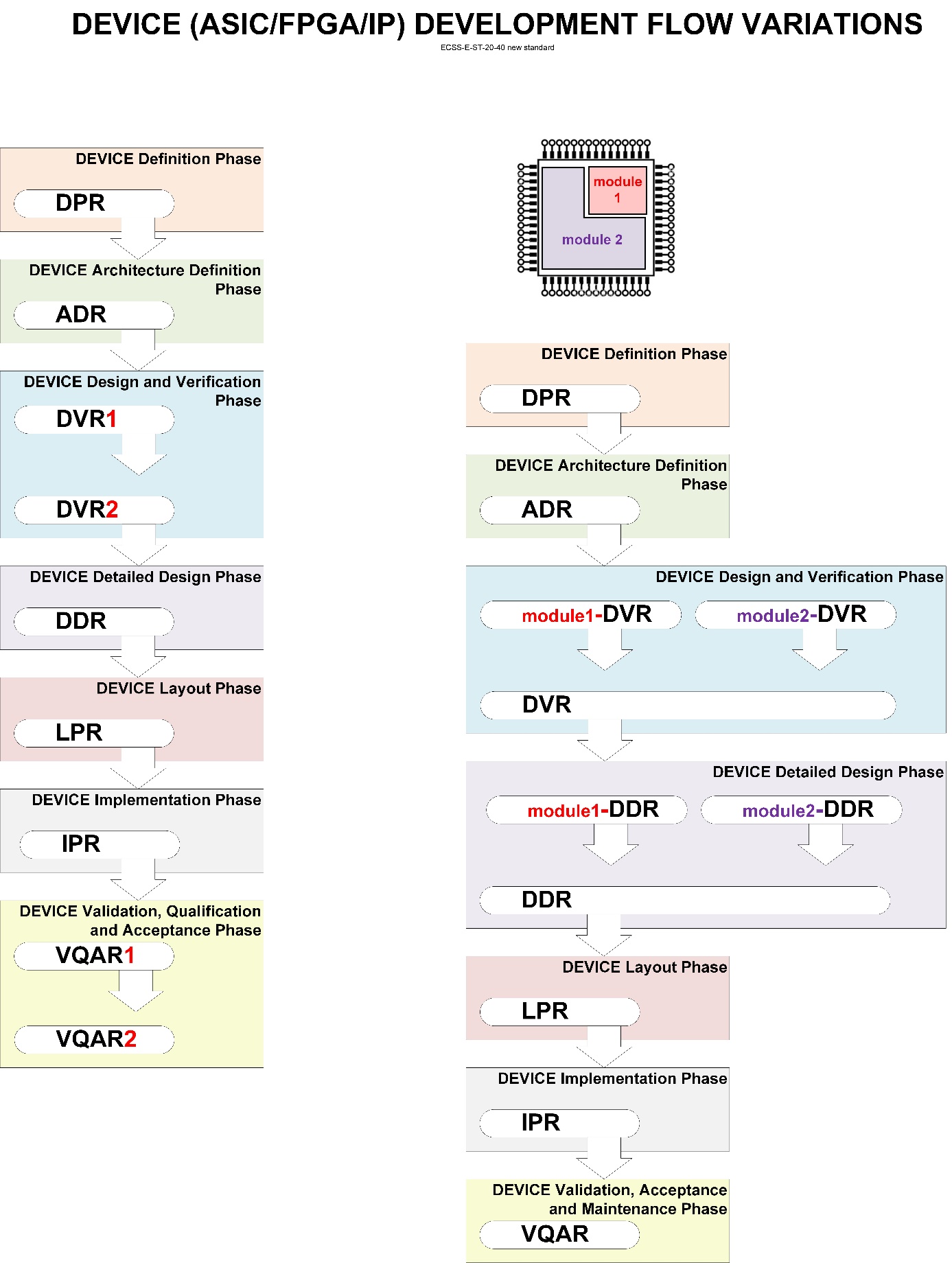 Figure: Example of DEVICE development flow with intermediate additional reviews
Parallel modules developments with integration step
Having parallel module developments with their own independent module documents and reviews, and then followed by a modules integration step which concludes with the corresponding top-level DEVICE phase review can be useful or necessary. This type of flow can be applied if different and distinct modules of the DEVICE are developed in parallel before they are connected and integrated into a single DEVICE. This implies that different design teams are developing in parallel different modules of the design.
An example of such a DEVICE development flow variation is shown in Figure J-2, where the DEVICE has two distinct modules that are developed in parallel during the DEVICE Design and Verification Phase, and further during the DEVICE Detailed Design Phase. As such, each module development has its own dedicated review in each phase, while there is also a final phase review where the entire integrated top-level DEVICE outputs for that phase are reviewed.
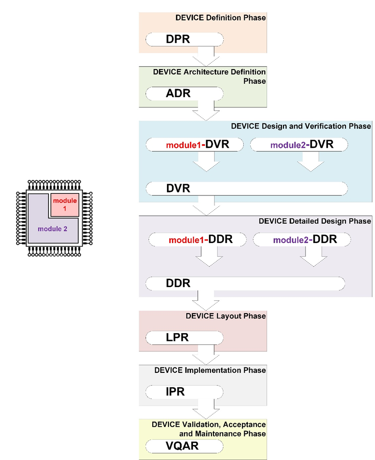 Figure: Example of DEVICE development flow variation with two DEVICE modules developed and reviewed in parallel
Phase merging
Merging two or more phases and having fewer reviews can be practical in some cases. For example, if the complexity of the DEVICE design is relatively low and fewer reviews are enough to confirm the good progress of the development. In other cases, the boundaries between the development work of some phases, as presented in the generic flow, is blurry.
For example, this is the case of full custom analogue ASIC developments, where the layout development effectively starts at the DEVICE Design and Verification Phase and can be seen as a continuous and often iterative design work until a final DEVICE layout is ready for the DEVICE Implementation Phase.
Likewise, for FPGAs the Layout Phase can be typically merged with the DEVICE Detailed Design Phase, and even sometimes with the DEVICE Design and Verification Phase if the design is not too complex and the time and costs of iterating until the DEVICE models are ready for DEVICE implementation are affordable to the project. The lower cost of DEVICE Implementation Phase of reprogrammable FPGAs, compared to the one of ASIC developments, can also facilitate and induce development flow iterations of the implementation phase and other phases too.
An example of such a DEVICE development flow variation is shown in Figure J-3, where the DEVICE Design and Verification Phase, the DEVICE Detailed Design Phase and the DEVICE Layout Phase have been merged into a larger phase with a single larger review at the end.
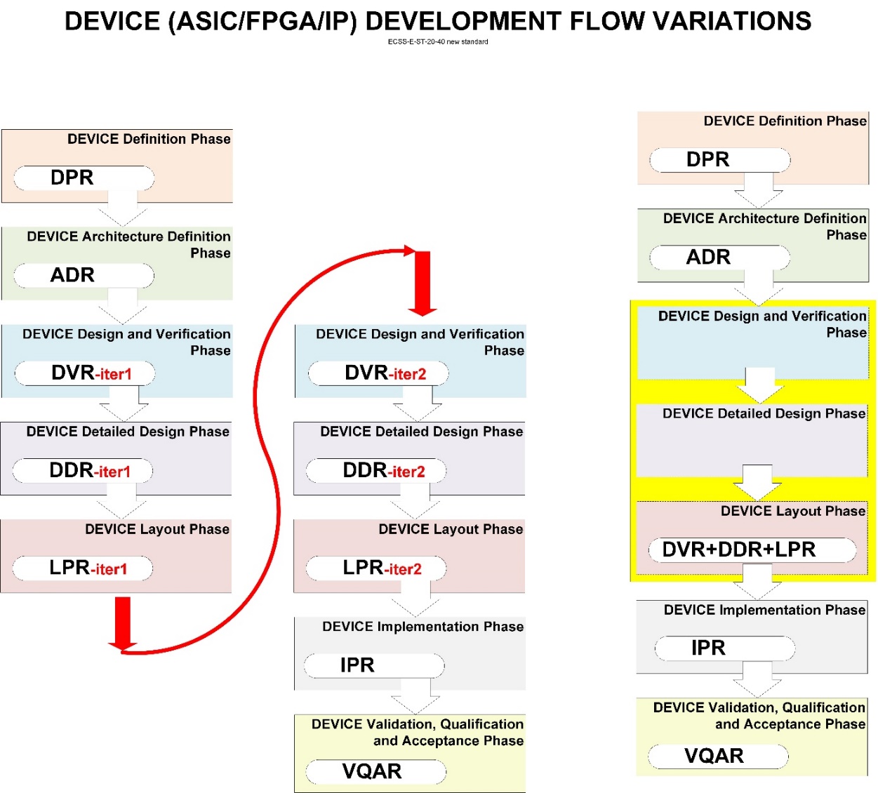 Figure: Example of DEVICE development flow variation where three phases have been merged
Phase iterations
Having phase iterations leading to updates of all phase outputs and to the repetition of the reviews of the repeated phases that can be useful or necessary in some DEVICE developments.
For example, due to unexpected and unresolvable poor simulation results at DEVICE Layout phase, it can be necessary to go back into the DEVICE Design and Verification Phase to rethink and change some parts of the architecture of netlist, or perhaps it can be enough to modify synthesis constraints to generate a different gate-level netlist, and thus just to iterate the DEVICE Detailed Design Phase. These iterations imply repeating the corresponding phase reviews as it can be in the example provided in Figure J-4.
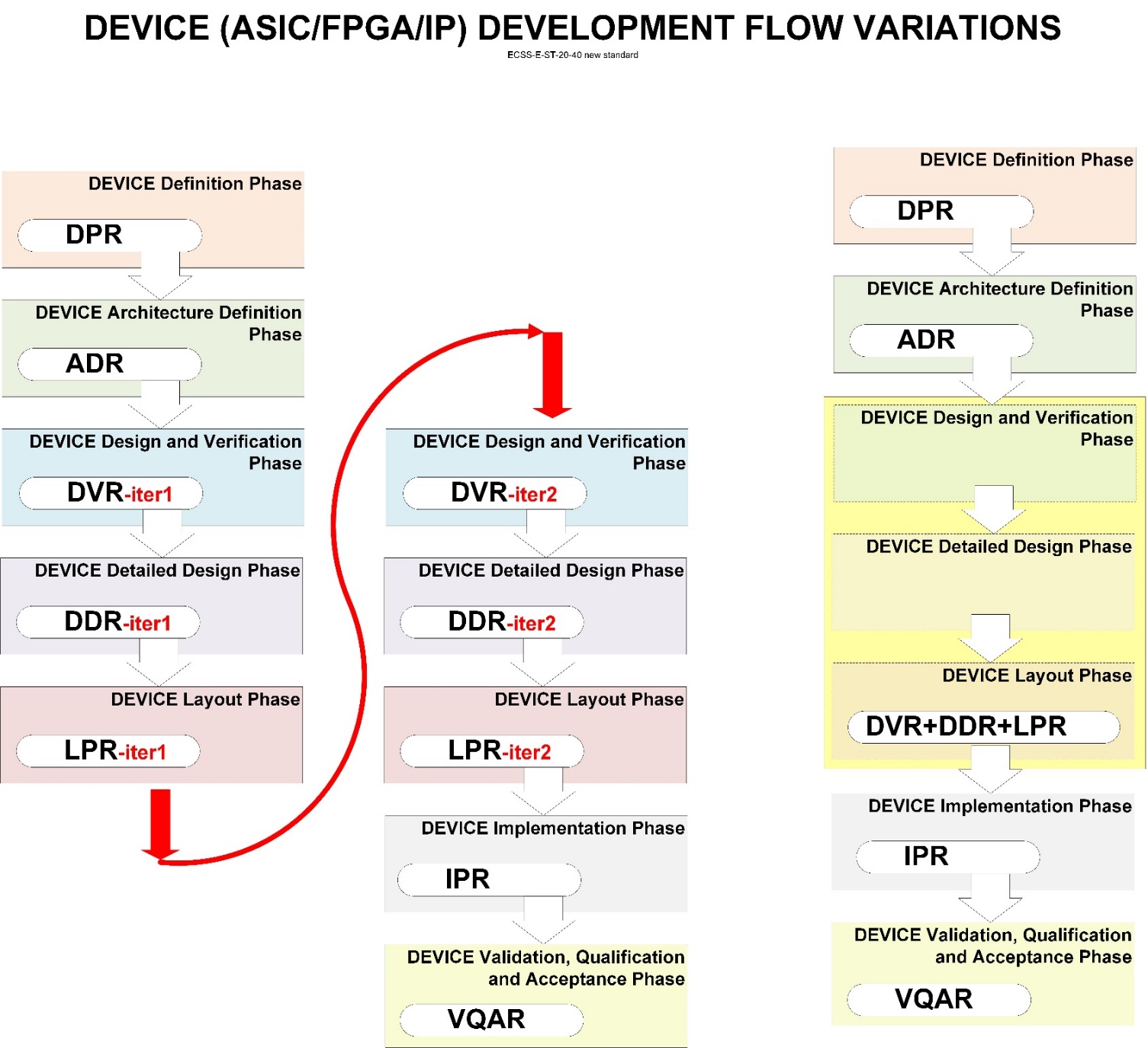 Figure: Example of DEVICE development flow where three phases are iterated
ANNEX(informative)DEVICE Development Expected Outputs
Various types of outputs are expected to be produced during the course of the development of a DEVICE and its different phases. Table K-1 is a summary of all these expected outputs of the engineering flow, including documents, DEVICE models and other database files, and hardware items. Table K-2 is a summary of all the document outputs expected at each review milestone for both, the engineering and the product assurance flows, as explained in ECSS-E-ST-20-40 and ECSS-Q-ST-60-03 respectively.
The DEVICE development contract defines what expected outputs are to be delivered, in which format and under which terms.
Table: Summary of expected outputs of engineering flow
|
Development phase
|
Documentation
|
DEVICE models and SW
|
Hardware
|
|
DEVICE Definition Phase
|
DEVICE Requirements Specification (DRS)
|
|
|
|
DEVICE Architecture Definition Phase
|
DEVICE Architecture Definition Report
|
|
|
|
DEVICE Design and Verification Phase
|
DEVICE Design Report
|
DEVICE Database containing: Simulation models (e.g. RTL)
|
|
|
DEVICE Detailed Design Phase
|
Netlist Generation Report
|
Updated DEVICE database containing:
|
|
|
DEVICE Layout Phase
|
Layout Generation Report
|
Updated DEVICE database containing:
|
|
|
DEVICE Implementation Phase
|
ASIC Production Tests Report
|
Updated DEVICE database containing:
|
Tested DEVICE(s)
|
|
DEVICE Validation, Qualification and Acceptance Phase
|
DEVICE Validation report
|
DEVICE Database (final)
|
Validation Tests hardware
|
Table: ECSS-E-ST-20-40 and ECSS-Q-ST-60-03 list of expected document outputs
|
Document
|
Document having a DRD annex
|
DEVICE Definition Phase Review
|
DEVICE Architecture Definition Phase Review
|
DEVICE Design and Verification Phase Review
|
DEVICE Detailed Design Phase Review
|
DEVICE Layout Phase Review
|
DEVICE
|
DEVICE Validation, Qualification and Acceptance Phase Review
|
|
The following notation is used:
| ||||||||
|
DEVICE Requirements Specification (DRS)
|
ECSS-E-ST-20-40
|
R
|
|
|
|
|
|
|
|
DEVICE Development Plan (DDP)
|
ECSS-E-ST-20-40
|
R
|
|
|
|
|
|
|
|
DEVICE Verification Plan (DVeP)
|
ECSS-E-ST-20-40
|
R
|
R
|
R
|
|
|
|
|
|
DEVICE Validation Plan (DVaP)
|
ECSS-E-ST-20-40
|
R
|
R
|
|
|
R
|
|
|
|
DEVICE Support and Maintenance Plan (DSMP) (conditional)
|
ECSS-E-ST-20-40
|
R
|
|
|
|
|
|
R
|
|
DEVICE Feasibility and Risk Assessment Report (DFRAR)
|
ECSS-E-ST-20-40
|
R
|
R
|
R
|
R
|
R
|
R
|
R
|
|
DEVICE Product Assurance Plan (DPAP)
|
ECSS-Q-ST-60-03 Annex A
|
B
|
|
|
|
|
|
|
|
DEVICE Product Assurance Report (DPAR)
|
ECSS-Q-ST-60-03 Annex B
|
R
|
R
|
R
|
R
|
R
|
R
|
R
|
|
DEVICE Reuse File (DRF)
|
ECSS-Q-ST-60-03 Annex C
|
R
|
R
|
R
|
R
|
R
|
R
|
R
|
|
Verification Control Document (VCD)
|
ECSS-E-ST-10-02 Annex B
|
R
|
R
|
R
|
R
|
R
|
R
|
B
|
|
Independent Verification Validation Plan (IVV Plan)
|
|
B
|
|
|
|
|
|
|
|
Configuration Management Plan (CMP)
|
ECSS-M-ST-40 Annex A
|
B
|
|
|
|
|
|
|
|
Configuration Item Data List (CIDL)
|
ECSS-M-ST-40 Annex C
|
B
|
|
|
|
|
|
|
|
DEVICE Architecture Definition Report
|
ECSS-E-ST-20-40
|
|
R
|
|
|
|
|
|
|
DEVICE Design Report
|
|
|
|
R
|
|
|
|
|
|
DEVICE Design Verification Report
|
|
|
|
R
|
|
|
|
|
|
DEVICE Data Sheet (conditional)
|
ECSS-E-ST-20-40
|
|
|
R
|
R
|
R
|
R
|
R
|
|
Netlist Generation Report
|
|
|
|
|
R
|
|
|
|
|
Netlist Verification Report
|
|
|
|
|
R
|
|
|
|
|
Layout Generation Report
|
|
|
|
|
|
R
|
|
|
|
Layout Verification Report
|
|
|
|
|
|
R
|
|
|
|
DEVICE Radiation Test Plan (conditional)
|
|
|
|
|
|
R
|
R
|
|
|
ESCC Detail Specification (conditional)
|
|
|
|
|
|
R
|
R
|
R
|
|
ASIC Production Tests Report
|
|
|
|
|
|
|
R
|
|
|
DEVICE Validation report
|
|
|
|
|
|
|
|
R
|
|
DEVICE Radiation Test Report (conditional)
|
|
|
|
|
|
|
|
R
|
|
DEVICE User Manual (conditional)
|
|
|
|
|
|
|
|
R
|
|
Experience Summary Report (conditional)
|
ECSS-E-ST-20-40
|
|
|
|
|
|
|
R
|
|
As-Built Configuration List (ABCL)
|
ECSS-M-ST-40 Annex D
|
|
R
|
R
|
R
|
R
|
R
|
B
|
|
Software Configuration File (SCF)
|
ECSS-M-ST-40 Annex E
|
R
|
R
|
R
|
R
|
R
|
R
|
B
|
|
Independent Verification Validation Report (IVV Report)
|
|
R
|
R
|
R
|
R
|
R
|
R
|
B
|
|
End Item Data Pack (EIDP)
|
ECSS-Q-ST-20 Annex B
|
|
|
|
|
|
|
B
|
ANNEX(informative) Equivalence of phase and milestone terminology of ECSS-M-ST-10 and ECSS-E-ST-20-40
The names of phases and reviews used in ECSS-E-ST-20-40 are different compared to the terminology used in ECSS-M-ST-10 standard.
Table L-1 summarizes and compares the terminology used in ECSS-M-ST-10 Space Project Management Project planning and implementation, and in ECSS-E-ST-20-40 ASIC, FPGA and IP Core engineering. The names of phases, reviews and outputs are listed in front of each other’s equivalent phase at system level, for ECSS-M-ST-10, and at DEVICE level, in ECSS-E-ST-20-40.
DEVICE development flow has no required phasing with system lifecycle.
Table: Equivalence of phase and milestone terminology of ECSS-M-ST-10 and ECSS-E-ST-20-40
|
ECSS-M-ST-10C
|
ECSS-E-ST-20-40C
| ||||
|
Phases
|
Reviews
|
outputs
|
outputs
|
Reviews
|
Phases
|
|
0
|
Mission Definition Review
|
NA
|
NA
|
NA
|
|
|
A
|
Preliminary Requirements Review
|
System (Equipment HW and SW, environmental) Requirements for the DEVICE
|
DEVICE Requirements Specification (DRS) DEVICE Feasibility and Risk Assessment Report (DFRAR) DEVICE Development Plan (DDP) DEVICE Verification Plan (DVeP) (preliminary) DEVICE Validation Plan (DVaP) (preliminary) DEVICE Support and Maintenance Plan (DSMP) (preliminary) DEVICE Verification Control Document (VCD) |
DEVICE Definition Phase Review (DPR) |
DEVICE Definition Phase |
|
B
|
System Requirements Review
| ||||
|
Preliminary Design Review
|
|
DEVICE Architecture Definition Report DRS (update) DVeP (update) DVaP (update) DFRAR (update) VCD (update) |
DEVICE Architecture Definition Phase Review (ADR) |
DEVICE Architecture Definition Phase |
|
|
DVeP (final) DEVICE Design Report DEVICE Design Verification Report DEVICE Data Sheet (preliminary) DEVICE database DFRAR (update) VCD (update) |
DEVICE Design and Verification Phase Review (DVR) |
DEVICE Design and Verification Phase |
|||
|
C
|
Critical Design Review (CDR) |
|
Netlist Generation Report Netlist Verification Report DEVICE Data Sheet (update) DEVICE Database (update) DFRAR (update) VCD (update) |
DEVICE Detailed Design Phase Review (DDR) |
DEVICE Detailed Design Phase |
|
|
Layout Generation Report Layout Verification Report DVaP (update) DEVICE Radiation Test Plan DEVICE Data Sheet (update) ESCC Detail Specification (preliminary) DEVICE database (update) DFRAR (update) VCD (update) |
DEVICE Layout Phase Review (LPR) |
DEVICE Layout Phase |
||
|
|
tested DEVICEs ASIC Production Tests Report FPGA Programming Test Report DEVICE database (update) DVaP (final) DEVICE Radiation Test Plan (final) DEVICE Data Sheet (update) ESCC Detail Specification (update) DFRAR (update) VCD (update) |
DEVICE Implementation Phase Review (IPR) |
DEVICE Implementation Phase |
||
|
D
|
Qualification Review (QR) |
|
DEVICE Validation Report DEVICE Radiation Test Report validated DEVICEs |
DEVICE Validation, Qualification and Acceptance Phase Review (VQAR) |
DEVICE Validation, Qualification and Acceptance Phase |
|
Acceptance Review (AR) |
|
DEVICE database (final) DEVICE Support and Maintenance Plan (final) Experience Summary Report DEVICE Data Sheet (final) ESCC Detail Specification (final) DEVICE User Manual DFRAR (update) VCD (final) |
|||
|
E
|
Operations Readiness Review (ORR) Flight readiness Review (FRR) Launch Readiness Review (LRR) Commissioning Result Review (CRR) End of Life Review (ELR) |
|
NA |
NA |
NA |
|
F
|
|
NA |
NA |
NA |
NA |
Bibliography
|
ECSS-S-ST-00
|
ECSS system – Description, implementation and general requirements
|
|
ECSS-E-ST-10-02
|
Space engineering - Verification
|
|
ECSS-M-ST-10
|
Space project management – Project planning and implementation
|
|
ECSS-M-ST-40
|
Space project management – Configuration and information management
|
|
ECSS-E-HB-20-40
|
Space engineering - Engineering techniques for radiation effects mitigation in ASICs and FPGAs handbook
|
|
ECSS-Q-ST-20
|
Space product assurance – Quality assurance
|
|
ECSS-Q-ST-60
|
Space product assurance – Electrical, electronic and electromechanical (EEE) components
|
|
ESCC 9000 - 2021
|
ESCC Generic Specification No. 9000 Integrated circuits: Monolithic and multichip microcircuits, wire-bonded, hermetically sealed and flip-chip monolithic microcircuits, solder ball bonded, hermetically and non-hermetically sealed and die
|
|
IEEE 1241-2010
|
Standard for Terminology and Test Methods for Analogue-to-Digital Converters
|
|
IEEE 1149.1-2013
|
Standard Test Access Port and Boundary-Scan Architecture
|