
Space engineering
Spacecraft discrete interfaces
Foreword
This Standard is one of the series of ECSS Standards intended to be applied together for the management, engineering and product assurance in space projects and applications. ECSS is a cooperative effort of the European Space Agency, national space agencies and European industry associations for the purpose of developing and maintaining common standards. Requirements in this Standard are defined in terms of what shall be accomplished, rather than in terms of how to organize and perform the necessary work. This allows existing organizational structures and methods to be applied where they are effective, and for the structures and methods to evolve as necessary without rewriting the standards.
This Standard has been prepared by the ECSS-E-ST-50-14C Working Group, reviewed by the ECSS Executive Secretariat and approved by the ECSS Technical Authority.
Disclaimer
ECSS does not provide any warranty whatsoever, whether expressed, implied, or statutory, including, but not limited to, any warranty of merchantability or fitness for a particular purpose or any warranty that the contents of the item are error-free. In no respect shall ECSS incur any liability for any damages, including, but not limited to, direct, indirect, special, or consequential damages arising out of, resulting from, or in any way connected to the use of this Standard, whether or not based upon warranty, business agreement, tort, or otherwise; whether or not injury was sustained by persons or property or otherwise; and whether or not loss was sustained from, or arose out of, the results of, the item, or any services that may be provided by ECSS.
Published by: ESA Requirements and Standards Division
ESTEC, ,
2200 AG Noordwijk
The
Copyright: 2008 © by the European Space Agency for the members of ECSS
Change log
|
ECSS-E-50-14A
|
First issue
|
|
ECSS-E-50-14B
|
Never issued
|
|
ECSS-E-ST-50-14C
|
Second issue
|
Scope
This standard specifies a common set of spacecraft onboard electrical interfaces for sensor acquisition and actuator control. The interfaces specified in this standard are the traditional point-to-point interfaces that are commonly used on modern spacecraft.
The interfaces specified in this standard include analogue and discrete digital interfaces used for status measurement and control, as well as point-to-point serial digital interfaces used for digital data acquisition and commanding of devices.
This standard specifies:
interface signal identification;
interface signal waveforms;
signal timing requirements;
signal modulation;
voltage levels;
input and output impedance;
overvoltage protection requirements;
bit ordering in digital data words;
cabling requirements where appropriate.
This standard does not cover:
connector requirements;
digital data word semantics;
message or block formats and semantics.
Connector requirements are not covered because these are normally mission or project specific. The goal of this standard is to establish a single set of definitions for these interfaces and to promote generic implementations that can be re-used throughout different missions.
When referred, the present standard is applicable as a complement of the already existing interface standards ANSI/TIA/EIA-422B-1994 and ITU-T Recommendation V.11 (Previously “CCITT Recommendation”) – (03/93).
Guidance for tailoring of the present standard can be found in Annex A.
This Standard may be tailored for the specific characteristics and constraints of a space project in conformance with ECSSSST-00.
Normative references
The following normative documents contain provisions which, through reference in this text, constitute provisions of this ECSS Standard. For dated references, subsequent amendments to, or revisions of any of these publications, do not apply. However, parties to agreements based on this ECSS Standard are encouraged to investigate the possibility of applying the most recent editions of the normative documents indicated below. For undated references the latest edition of the publication referred to applies.
|
ECSS-S-ST-00-01
|
ECSS system - Glossary of terms
|
|
ANSI/TIA/EIA-422B-1994
|
Electrical characteristics of balanced voltage digital interface circuits
|
|
ITU-T Recommendation V.11 (Previously “CCITT Recommendation”) – (03/93)
|
Electrical characteristics for balanced double-current interchange circuits operating at data signalling rates up to 10 Mbit/s
|
This document is technically equivalent to ANSI/TIA/EIA/422B-1994.
Terms, definitions and abbreviated terms
Terms from other standards
For the purpose of this Standard, the terms and definitions from ECSSST0001 apply.
Terms specific to the present standard
accuracy
closeness of a measurement to the actual quantity being measured
For the purposes of this Standard it is expressed as percentage of the full measurement range or as an absolute value.
circuit
conducting path which conveys a signal across the interface from the signal source to the signal destination
A circuit includes the cable conductor, any intervening connectors, and any circuit elements such as protection resistors and coupling capacitors, which make up the signal path.
DHS data interchange bus
underlying communication medium which connects the DHS core elements
This can consist of more than one physical bus.
DHS core element
component of a data handling system which has a direct connection to the DHS data interchange bus
E.g.: bus controllers and remote terminals.
DHS peripheral element
component of a data handling system which does not have a direct connection to the DHS data interchange bus
E.g.: sensors and actuators.
ground displacement voltage
voltage difference between source and receiver ground references
Users are encouraged to use this definition instead of ‘common mode voltage’ that is not correct when referring to the academic definition.
time reference point
point at which a time interval starts or ends
It is the mid point between the nominal high and nominal low signal voltages.
Abbreviated terms
For the purpose of this standard, the abbreviated terms of ECSS-S-ST-00-01 and the following apply:
|
Abbreviation
|
Meaning
|
|
A/D
|
analogue to digital
|
|
ADC
|
analogue digital converter
|
|
ASM
|
analogue signal monitor
|
|
BDM
|
bi-level discrete monitor
|
|
BSD
|
bi-directional serial digital
|
|
BSM
|
bi-level switch monitor
|
|
CM
|
common mode
|
|
DHS
|
data handling system
|
|
HPC
|
high power command
|
|
HC-HPC
|
high current high power command
|
|
HV-HPC
|
high voltage high power command
|
|
ISD
|
input serial digital
|
|
LPC
|
low power command
|
|
LPC-P
|
low power command, pulsed
|
|
LPC-S
|
low power command, static
|
|
LSB
|
least significant bit
|
|
LV-HPC
|
low voltage high power command
|
|
MSB
|
most significant bit
|
|
OBDH
|
on-board data handling
|
|
OSD
|
output serial digital
|
|
TSM
|
temperature sensors monitor
|
Conventions
Bit numbering convention
The most significant bit of an n-bit field is:
numbered bit 0 (zero),
the first bit transmitted, and
the leftmost bit on a format diagram.
The least significant bit of an n-bit field is:
numbered bit n-1,
the last bit transmitted, and
the rightmost bit on a format diagram.
This convention is illustrated in Figure 31.
 Figure 31: Bit numbering convention
Timing diagram conventions
Timing diagrams are always drawn with the earliest time on the left and time advancing to the right.
Where an event, such as a transition, in one signal causes an event in another, the two events are linked by an arrow with the tail of the arrow on the causal event and the head of the arrow on the resultant event.
Where an event in one signal is the result of an event in another signal and a qualifying condition in one or more other signals, the connecting arrow is associated with the governing condition using a bull’s eye.
These conventions, together with other timing diagram symbols, are shown in Figure 32.
 Figure 32: Timing diagram conventions
Signal and signal event naming convention
Signals are named in a manner which indicates the function of that signal. For example, a clock used for data bit sampling can be called DATA_CLK.
Control signal naming is meaningful with the function of the signal, its direction, and its assertion levels all indicated. The direction is indicated with respect to the DHS core element so that an OUT signal is an output, i.e. driven from the core element. An IN signal is an input to the core element. For example, a signal carrying data out of the core element is named DATA_OUT.
Control signal assertion or validity levels are indicated within brackets. For example, a gate output signal which is asserted when low is named GATE_OUT(L). Similarly, an input signal which indicates that a device is ready when it is high is named READY_IN(H).
Signal events such as transitions and pulses are also named symbolically using “UP“ and “DOWN“ indication. For example, STARTUP indicates a rising edge event on the start signal, and STOPDOWN indicates a falling edge on the stop signal. RUNUPDOWN indicates a positive going pulse on the run signal, while HALTDOWNUP indicates a negative going pulse on the halt signal.
Signal timing and measurement references
Signal rise and fall times, which are shown in Figure 33, are measured between 10 % and 90 % of the difference between the nominal low and nominal high signal voltages, as it can be seen in the mentioned figure.
 Figure 33: Signal timing and measurement references
General
Introduction
This standard defines electrical interfaces for use onboard spacecraft to connect simple devices such as sensors and actuators to the data handling system. The interfaces defined are:
analogue signal interfaces (clause 5)
analogue signal monitor
temperature sensor monitor
bi-level discrete input interfaces (clause 6)
bi-level discrete monitor
bi-level switch status monitor
command interfaces (clause 7)
high power pulse command
low power command
serial digital interfaces (clause 8).
Each interface is defined in terms of the electrical and timing characteristics of the signals comprising that interface. Connectors for the interfaces are not defined because these are often highly project dependent. Cabling characteristics are defined where appropriate.
For the serial digital interfaces, the data content of the digital words is not defined since this is the subject of higher level protocol standards beyond the scope of this Standard.
Unless otherwise stated, specified performances are applicable when both source and receiver are powered.
Architectural concepts
Overview
The interfaces specified in this Standard are intended to connect DHS core elements to DHS peripheral elements as shown in Figure 41. However, there are no technical reasons to prevent these interfaces being used between core elements where it is appropriate to do so, and this Standard does not preclude such a configuration.
A peripheral element can have more than one user interface and also user interfaces of different types, depending on its function and design. For example, some sensors can set threshold levels or sensitivities by means of data written to them. In this case that sensor can use an output serial digital interface to write the data in addition to an input serial digital interface to read the sensor value. Alternatively, some devices are signalled to indicate that they are commanded to acquire a data sample. In that case they can use a serial digital interface together with a pulse interface.
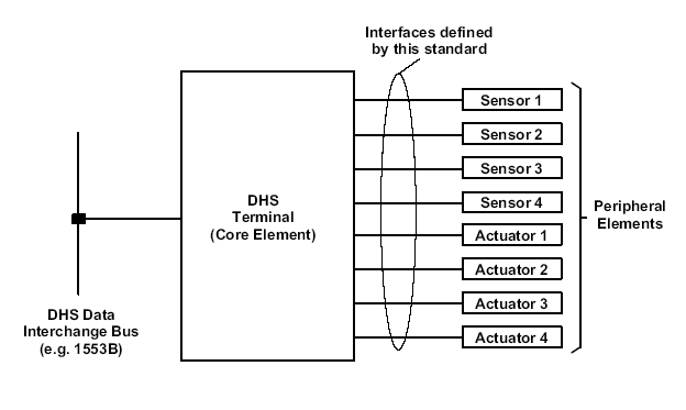 Figure 41: Architectural context of interfaces defined in this standard
General failure tolerance
Input interfaces
Among other failure cases, receivers shall:
- Not be stressed and not show degraded performance when input is open circuit except on the input I/F that is open circuit.
- Not be stressed and not show degraded performance when input is short circuit to ground except on the input I/F that is short circuit.
No specific performance requirements are imposed while in this status.
Output interfaces
Among other failure cases, transmitters shall:
- Not be stressed and not show degraded performance when output is open circuit except on the output I/F that is open circuit.
- Not be stressed when output is short circuit to ground.
No specific performances requirement is imposed while in this status.
Interface control during power cycling
Input interfaces
Input interfaces shall not be damaged or harmed during power cycling conditions taking the transmitting side state into account in any normal state or applicable failure condition.
Receivers shall not deliver power to the other circuits or be stressed when the unit is OFF while connected to an active driver.
No specific performance requirements are imposed while in this status.
Output interfaces
Output interfaces shall not be damaged or harmed during power cycling conditions when the receiving side state is in any normal state or specified failure condition.
No specific performance requirements are imposed while in this status.
For pulse commands it shall be ensured that spurious commands are not emitted during power cycling that exceed activation limits for the receivers.
- 1 For pulse commands, see Clause 7.
- 2 This requirement does not specify the prevention of spurious pulses, but ensures either that:
- spurious pulses are below the threshold for the receiver, or
- the spurious pulse duration is short enough to not drive the load into activation (for example a relay coil or opto-coupler diode).
Cross-strapping
General
For 2 units (UNIT_1 & UNIT_2), that can be used in redundancy, the cross-strapping of drivers and receivers shall be as specified in Figure 42, and meet the following conditions:
- The UNIT_2_A I/F is capable to receive:
- A signal from the UNIT_1_A I/F through a dedicated link
- A signal from the UNIT_1_B I/F through a dedicated link
- The UNIT_2_B I/F shall is capable to receive:
- A signal from the UNIT_1_A I/F through a dedicated link
- A signal from the UNIT_1_B I/F through a dedicated link
- The UNIT_1_A I/F is capable to deliver:
- A signal to the UNIT_2_A I/F through a dedicated link
- A signal to the UNIT_2_B I/F through a dedicated link
- The UNIT_1_B I/F is capable to deliver:
- A signal to the UNIT_2_A I/F through a dedicated link.
- A signal to the UNIT_2_B I/F through a dedicated link.
To achieve full cross-strapping benefits, in terms of reliability, any potential common failure of UNIT_1_A and UNIT_1_B drivers and UNIT_2_A and UNIT_2_B receivers shall be avoided.
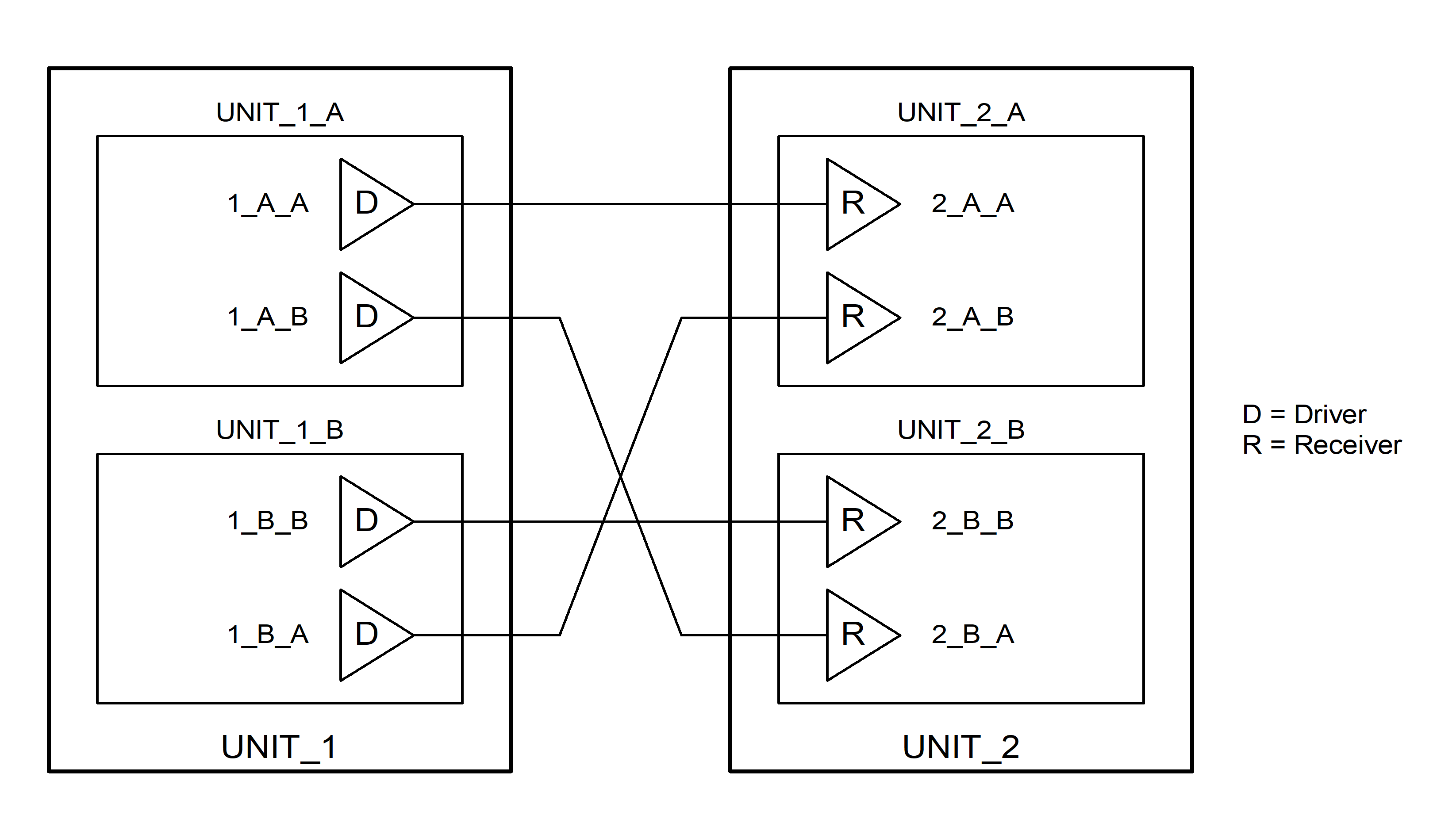 Figure 42: General scheme of redundant unit’s cross-strapping
Immunity at UNIT_2 level
Under the condition (Receiver = ON linked to Transmitter = OFF of UNIT_1), in the configuration where UNIT_1 driver is OFF and UNIT_2 receiver is ON, the information received by this receiver shall not disturb the valid information received by the other receiver (linked to a Transmitter ON).
In this configuration the electrical status at receiver output is stable (due to hysteresis) but possibly unknown (logical "1" or "0").
It should be ensured that any input signal is in a known (inactive) stable state when driver is OFF.
If 4.2.4.2b is not met, a validation / inhibition stage at the receiver output of UNIT_2 should be implemented.
For example, the validation of the path can be made by a dedicated direct command arriving from UNIT_1, which inhibits the UNIT_2 receiver output unused (if such a configuration has been thoroughly designed with respect to failure cases).
Protections at UNIT_1 driver level
Under the condition (Transmitter = OFF linked to Receiver = ON of UNIT_2), whether powered or not, UNIT_1 drivers shall withstand any receiver characteristics as described in Clauses 5 to 8.
Protections at UNIT_2 receiver level
Under the condition (Receiver = OFF linked to Transmitter = ON of UNIT_1), whether powered or not, UNIT_2 receivers shall withstand any driver characteristics as described in Clauses 5 to 8.
Harness cross-strapping
Overview
Harness cross-strapping is applied when heritage units, without classical cross-strapping interfaces, are used, in the case that a single redundant unit is interfaced to both a nominal and redundant system. If the spacecraft is severely mass-limited, harness cross-strapping can be used instead.
Harness cross-strapping can be used in two configurations:
Single source – Dual receiver configuration, as shown in Figure 43.
Dual source – Single receiver configuration, as shown in Figure 44.
The Single source – Dual receiver configuration is typically applied for BSM interfaces as described in clause 6.2.
The Dual source – Single Receiver configuration is typically applied for HPC interfaces as described in clause 7.1.
Note that this harness cross-strapping can be performed by galvanic connections in harness, as indicated in Figure 43 and Figure 44. However, the equivalent configuration applies in case the physical inter-connection is performed either within the source or within the receiver unit. The general rules and protections as mentioned in this clause 4.2.5 apply then also for those cases.
Possible problems that can be introduced by harness cross-strapping include failure propagation, loading and leakage injection of the active I/F by the redundant, inactive circuit such that the active circuit does not meet its performance requirements, incompatibility of protection circuitry of a given circuit with either the Receiver I/F circuit or the Driver (see Figure 44) I/F circuit. Note that in general it is important to consider loading by the redundant, inactive circuit also when powered off, even if the inactive circuit is normally powered (hot redundancy).
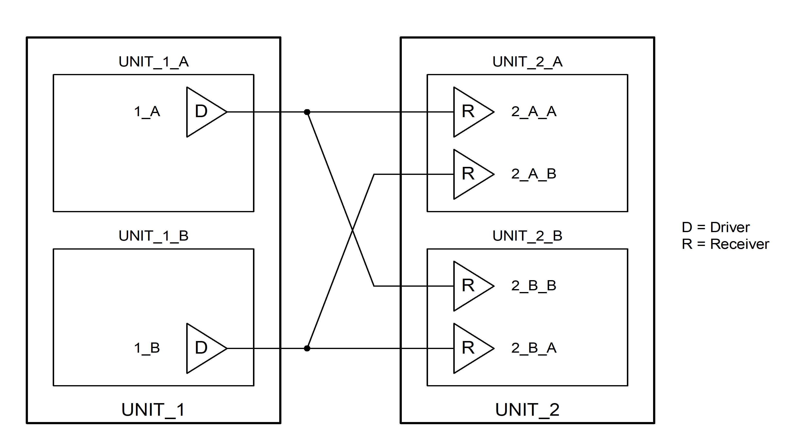 Figure 43: Example scheme for Single source – Dual receiver cross-strapping
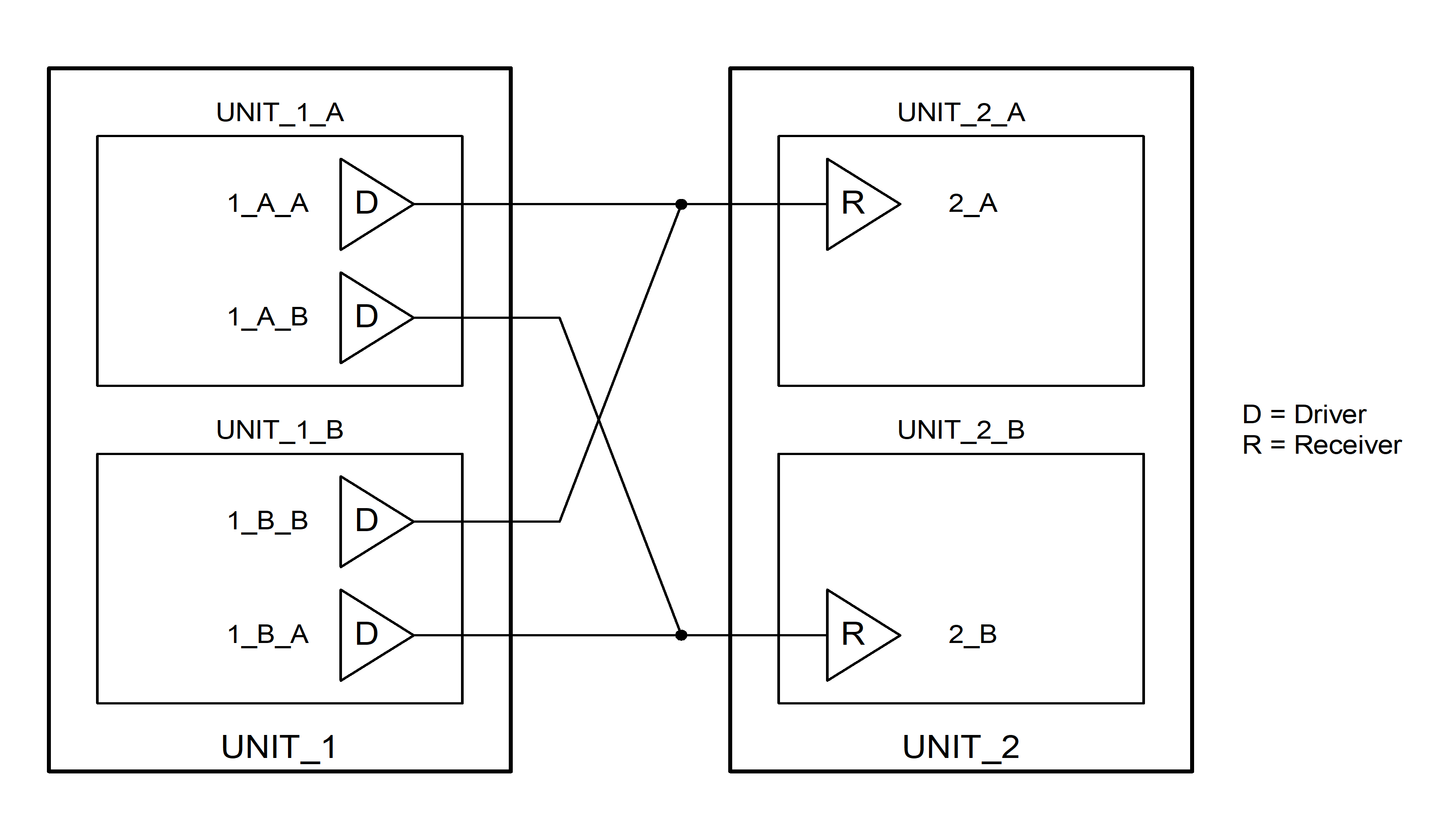 Figure 44: Example scheme for Dual source – Single receiver cross-strapping
Provisions
If harness cross-strapping is used, there shall be no mechanism whereby the failure of either the receiver or unit interface can propagate to the I/F of another, unrelated unit.
This requirement refers to a common mode failure where a failure of one interface then propagates inside the receiver thereby affecting units unrelated to the original failure.
If harness cross-strapping is used, the calculation of the overall system reliability shall include the potential degradation or damage of the I/F of a redundant unit due to the failure of other interface.
This requirement refers to the failure on a nominal unit causing the inoperability of the cross-strap. This means that there is a reduction in the possible reliability of the cross-strap.
If harness cross-strapping is used, the capability shall be provided to shut down the inoperable unit regardless of the failure mode
This implies that the power can be removed from the unit by independent means such as disabling the power interface at the power distribution unit (e.g. with the means described in clause 4.2.4.2)
Under the condition (Transmitter = OFF linked to Receiver = ON of UNIT_2), whether powered or not, UNIT_1 drivers shall withstand any receiver characteristics as described in Clauses 5 to 8.
Under the condition (Receiver = OFF linked to Transmitter = ON of UNIT_1), whether powered or not, UNIT_2 receivers shall withstand any driver characteristics as described in Clauses 5 to 8.
Cable capacitance
It is important that the DHS interfaces consider the capacitive loading by the harness. Figure 45 defines the capacitances involved for a twisted shielded pair cable.
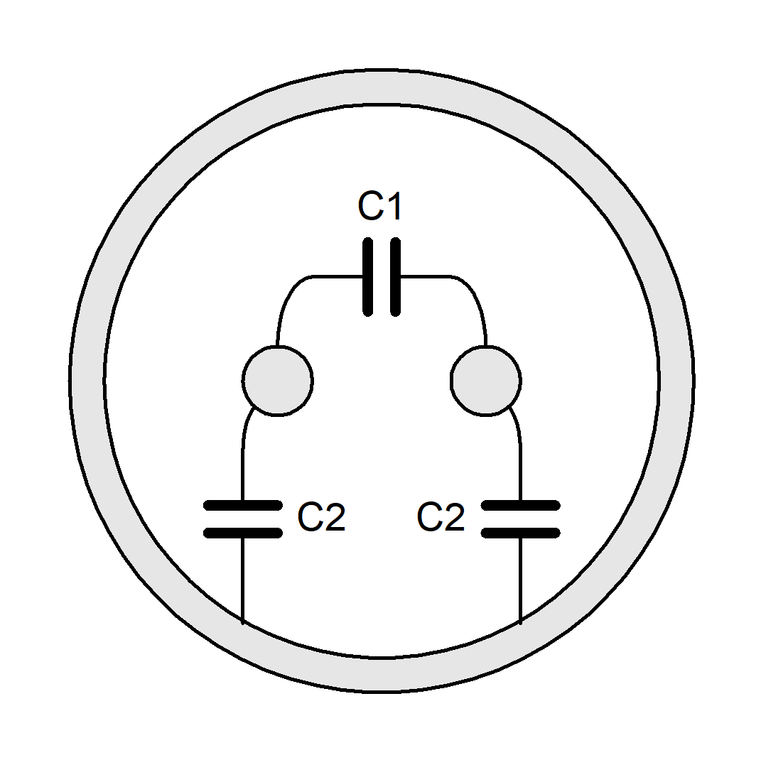 Figure 45: Cable capacitance definitions
Effective capacitances can then be calculated according to:
Core to core capacitance ![]()
Core to shield capacitance ![]()
Core to core capacitance with shield connected to one core ![]()
Note that the latter case applies typically when either the source or the receiver is single ended, which implies that both the shield and one of the core wires are grounded.
Analogue signal interfaces
Overview
The analogue signal interfaces are used for direct connection to a device which produces a continuous variable analogue voltage to indicate the value of the parameter being measured.
Usually, the analogue voltage produced by the sensor or a peripheral element is converted into a digital value within the core element to which it is connected. This Standard specifies the electrical characteristics of the analogue signal interfaces.
Two types of analogue interfaces are specified:
Analogue signal monitor interface, ASM (see 5.2)
Temperature sensors monitor interface, TSM (see 5.3)
Analogue signal monitor (ASM) interface
General
Overview
The analogue signal monitor interface is based on differential receiver circuit where both the high and low analogue signal lines are floating with respect to the receiver signal ground; the source interface can be either single ended or differential.
The analogue voltage provided is sampled intermittently by the core element. The precise frequency and the duration of the sampling interval depend on the A/D conversion service being used. However, the input impedance and capacitance exhibited by an analogue signal interface can differ when the input signal is actually being sampled compared with when it is not. As a consequence, different input impedance and capacitance requirements are provided for the different configurations.
In addition, the impedance seen when the receiver element is powered off is specified.
Basic application scenario
The interface specified in this clause 5.2.1.2 is defined on the basis of a typical analogue signal monitoring application scenario, i.e.
differential voltage range: 0 to 5 V or optionally 0 to 5,12 V;
signal bandwidth: ≤ 1 Hz;
This means that accuracy requirements are specified here assuming only slowly changing (quasi-static) signals. That does not prohibit, for instance, rapid transitions in signals, but accuracy is unspecified during such events.
ground displacement voltage: ≤ ±1 V in the frequency range 0 to 1 kHz, falling at 20 dB per decade up to 1 MHz;
conversion resolution: 12 bits.
- 1 The specified 12 bits resolution is not incompatible with use of ADC having 14 or even 16 bits resolution. In that case, LSB are "not significant".
- 2 Even if the overall channel accuracy requirement in 5.2.1.4 can be met also with an 8 bit ADC, it is important to note that in this case the ADC quantization error contributes ±0,2 % to the overall channel accuracy, thus normally a good practice is to use a 12 bit ADC.
Applications other than the basic scenario
If the actual scenario differs from the one defined in 5.2.1.2, the interface shall not be directly used.
- 1 For example, if the specific application uses higher conversion accuracy or has different operational conditions, e.g. higher displacement.
- 2 In particular, ground displacement heavily affects the achievable conversion accuracy. Different scenario or specified performances can, for instance, ask for source impedance balancing.
The modified interface shall be supported by an analysis of the overall system, including both interface source and receiver as well as interconnecting wiring.
Acquisition of the analogue channels by the core element
The errors introduced by the DHS receiver analogue acquisition chain, including temperature, ground displacement voltage rejection, A/D conversion inaccuracy, herein specified source impedance and cable capacitance, supply voltage variations, lifetime and radiation effects shall be less than 1 % of the full scale.
Analogue signal monitor interface
Source circuit
The source circuit shall meet the characteristics specified in Table 51.
Table 51: Analogue signal monitor source circuit characteristics
|
Reference
|
Characteristic
|
Value
|
|
5.2.2.1 a.1
|
Circuit type
|
Single ended or differential
|
|
5.2.2.1 a.2
|
Transfer
|
DC coupled
|
|
5.2.2.1 a.3
|
Zero reference
|
Signal ground – in case of differential source (ref Figure 52), the return signal’s potential shall be equal to unit’s chassis ground.
|
|
5.2.2.1 a.4(a)
|
Nominal output voltage range, Vout
|
0 V to +5 V a
|
|
5.2.2.1 a.4(b)
|
0 V to +5,12 V
| |
|
5.2.2.1 a.5
|
Output impedance, Zout
|
5 k
|
|
5.2.2.1 a.6
|
Fault voltage tolerance, Vsft
|
-17,5 V to +17,5 V with an overvoltage source impedance > 1,0 k
|
|
5.2.2.1 a.7
|
Fault voltage emission, Vsfe
|
-16,5 V to +16,5 V
|
|
a The range 0 V – 5 V is the preferred one. 5,12 V can be used if straightforward A/D conversion is necessary.
| ||
Receiver circuit
The receiver circuit shall meet the characteristics specified in Table 51.
Table 52 Analogue signal receiver circuit characteristics
|
Reference
|
Characteristic
|
Value
|
|
5.2.2.2 a.1
|
Circuit type
|
Differential
|
|
5.2.2.2 a.2
|
Transfer
|
DC coupled
|
|
5.2.2.2 a.3(a)
|
Nominal input voltage range, Vin
|
differential: 0 V to +5 V a
|
|
5.2.2.2 a.3(b)
|
differential: 0 V to +5,12 V
| |
|
5.2.2.2 a.4
|
Ground displacement voltage, VGD
|
-1 V to 1 V up to 1 kHz rolling-off at 20 dB/decade up to 1 MHz
|
|
5.2.2.2 a.5
|
Differential input impedance (sampling), Zis
|
1 M
|
|
5.2.2.2 a.6
|
Differential input impedance (not sampling), Zins
|
10 M
|
|
5.2.2.2 a.7
|
Differential input impedance (powered off), Zioff
|
10 k
|
|
5.2.2.2 a.8
|
Differential input capacitance (sampling), Cis
|
1,5 F
|
|
5.2.2.2 a.9
|
Differential input capacitance (not sampling), Cins
|
1,5 F
|
|
5.2.2.2 a.10
|
Differential input capacitance (powered off), Cioff
|
1,5 F
|
|
5.2.2.2 a.11
|
Fault voltage emission, Vrfe
|
-16,5 V to +16,5 V with a series impedance 1,0 k
|
|
5.2.2.2 a.12
|
Fault voltage tolerance, Vrft
|
-17,5V to +17,5 V
|
|
a The range 0 V – 5 V is the preferred one. 5,12 V can be used if straightforward A/D conversion is necessary
| ||
Harness
Wire type
The wire type should be twisted shielded lines.
If 5.2.2.3.1a is not met, n-tuples shall be used.
The shield shall be connected to the structure ground both on source and receiver sides.
Core to shield capacitance
The capacitance CCT shall be less than 2 nF.
Interface arrangement
The electrical interface arrangement is depicted in Figure 51 and Figure 52, which show specific implementation to be taken as examples, but other implementations compliant to requirements are not excluded.
 Figure 51: Analogue signal monitor (single ended source) interface arrangement
 Figure 52: Analogue signal monitor (differential source) interface arrangement
Temperature sensors monitor (TSM) interface
Overview
Temperature monitor channels are resistance measurement channels used for resistive temperature sensor acquisition.
The word "thermistor" is derived from the description "thermally sensitive resistor". Thermistors are further classified as "Positive Temperature Coefficient" devices (PTC devices) or "Negative Temperature Coefficient" devices (NTC devices):
PTC devices are devices whose resistance increases as their temperature increases.
NTC devices are devices whose resistance decreases as their temperature increases.
Two types of temperature monitor channels are addressed herein, referring to the two main classes of transducers available on the market:
TSM1: Wide range resistance acquisition, suitable for NTC thermistors (negative temperature characteristic).
TSM2: Limited range resistance acquisition, suitable for platinum (PT) type.
The conditioning configuration to be used depends on the transducer used. Both TSM1 and TSM2 interfaces are specified in terms of resistance measurement accuracy.
TSM1 can be used for platinum type sensors (PT), but that generally shows worse accuracy than a well adapted TSM2. Also, TSM2 can be used for NTC type of sensor, but the temperature range is then restricted.
Examples of corresponding measurement error in terms of temperature are given in clause 5.3.5.5.
TSM acquisition layout
The thermistors shall be powered by the receiver, and
The resulting voltage shall be utilised to feed a dedicated analogue channel.
The objective of these requirements is that the receiver is able to directly interface with a passive thermistor:
TSM acquisition resolution
At least 12-bit resolution shall be used.
Even if the overall channel accuracy requirement can be met also with an 8-bit ADC, it is important to note that in this case the ADC quantization error alone contributes ±0,2% to the overall channel accuracy.
TSM wire configuration
Dedicated input and return line from the current source to each thermistor channel shall be provided.
TSM electrical characteristics
TSM1
Overview
The TSM1 interface has the following features:
The measurable resistance range is specified from 0 to .
The interface is normalized with a parameter RNORM (), selectable within a specific range, where RNORM is the resistance of the thermistor at a specified temperature point, where the highest temperature measurement accuracy is needed (the centre of the measurement range).
RNORM is selected per group of channels as a function of the sensor type and the temperature range of interest.
The specified accuracy is expressed as a maximum error x.
The specified accuracy in terms of resistance is obtained from a formula including RNORM and x.
The resistance accuracy is specified at the DHS unit terminals, i.e. excluding any error contribution from the thermistor or harness.
TSM1 error model
The maximum error in Rth, Rth, shall be calculated as follows:
![]() , if RNORM > x(Rth + RNORM),
, if RNORM > x(Rth + RNORM),
![]() otherwise
otherwise
This calculation is based on the model of the TSM1 interface shown in Figure 53. Rth(T) symbolizes the resistance of the thermistor as a function of temperature T.
The output from the ADC, x, has the range 0 to 1. The formula to express x as a function of Rth(T) is then:
![]() Figure 54 shows how the relative error in Rth, Rth/Rth, varies with Rth with examples of RNORM and x.
Figure 54 shows how the relative error in Rth, Rth/Rth, varies with Rth with examples of RNORM and x.
Examples have been evaluated for some specific thermistor types in clause 5.3.5.5, showing the error in terms of temperature.
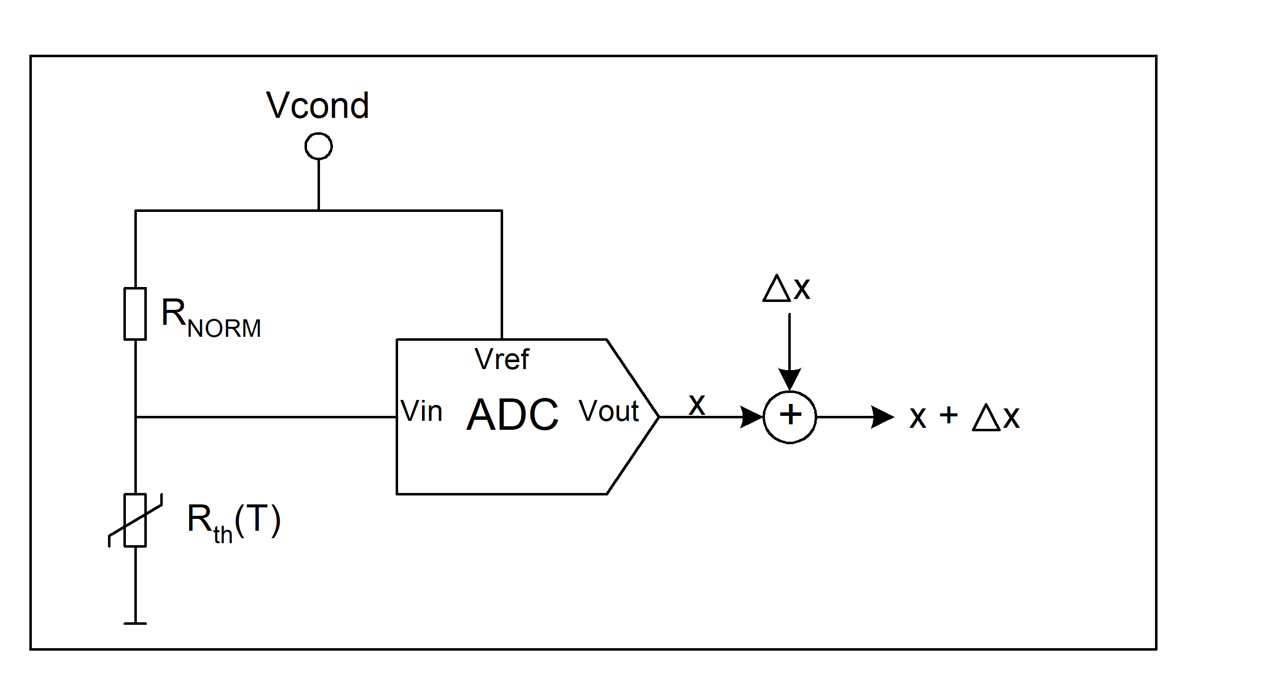 Figure 53: TSM1 reference model
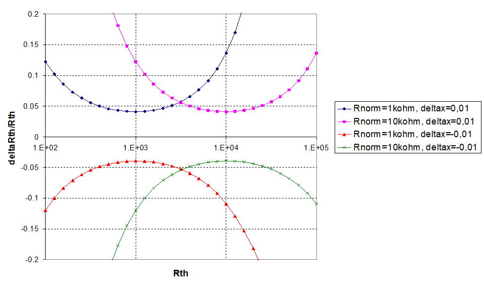 Figure 54: Requirement for Rth/Rth as a function of RNORM and Rth. x = ±0,01
TSM1 source electrical characteristics
The characteristics in Table 53 shall be provided.
Table 53: TSM1 source circuit characteristics
|
Reference
|
Characteristic
|
Value
|
|
5.3.5.1.3 a.1
|
Circuit type
|
Floating Resistive sensor
|
|
5.3.5.1.3 a.2
|
Transfer
|
DC coupled
|
|
5.3.5.1.3 a.3
|
Resistance range, Rs
|
0 to Ω
|
|
5.3.5.1.3 a.4
|
Fault voltage tolerance, Vsft
|
-17,5 V to +17,5 V with an overvoltage source impedance ≥ 1 kΩ
|
TSM1 receiver electrical characteristics
The characteristics in Table 54 shall be provided.
Table 54: TSM1 receiver circuit characteristics
|
Reference
|
Characteristic
|
Value
|
|
5.3.5.1.4 a.1
|
Circuit type
|
Single ended receiver with multiplexed inputs
|
|
5.3.5.1.4 a.2
|
Transfer
|
DC coupled
|
|
5.3.5.1.4 a.3
|
Sensor injected power, Pi
|
≤ 1 mW
|
|
5.3.5.1.4 a.4
|
Measurement error, x
|
< ±0,01
|
|
5.3.5.1.4 a.5
|
Parameterized resistance range, RNORM
|
1 kΩ, to 10 kΩ, to be specified per group of channels
|
|
5.3.5.1.4 a.6
|
Fault voltage emission, Vrfe
|
-16,5 V to +16,5 V with a source impedance of ≥ 1kΩ
|
|
5.3.5.1.4 a.7
|
Fault resistance tolerance, Rrft
|
Short circuit to ground
|
|
NOTE The low resistance range of RNORM is suitable for TSM receiver systems using power switched thermistor conditioning, where low impedance is of special interest to achieve fast settling. The high resistance range of RNORM is more suitable for TSM receiver systems using continuous thermistor conditioning, where low power is crucial, but fast settling is of less concern
| ||
Harness
The wiring type shall be twisted n–tuple.
The capacitance CCC measured between the two core wires shall be less than or equal to 1 nF.
Interface arrangement
The electrical I/F arrangement is specified in Figure 55.
- 1 Circuitry and resistors are indicative only; other implementations meeting the above requirements are not excluded.
- 2 � In practical implementations a resistance to ground in the receiver is often used.
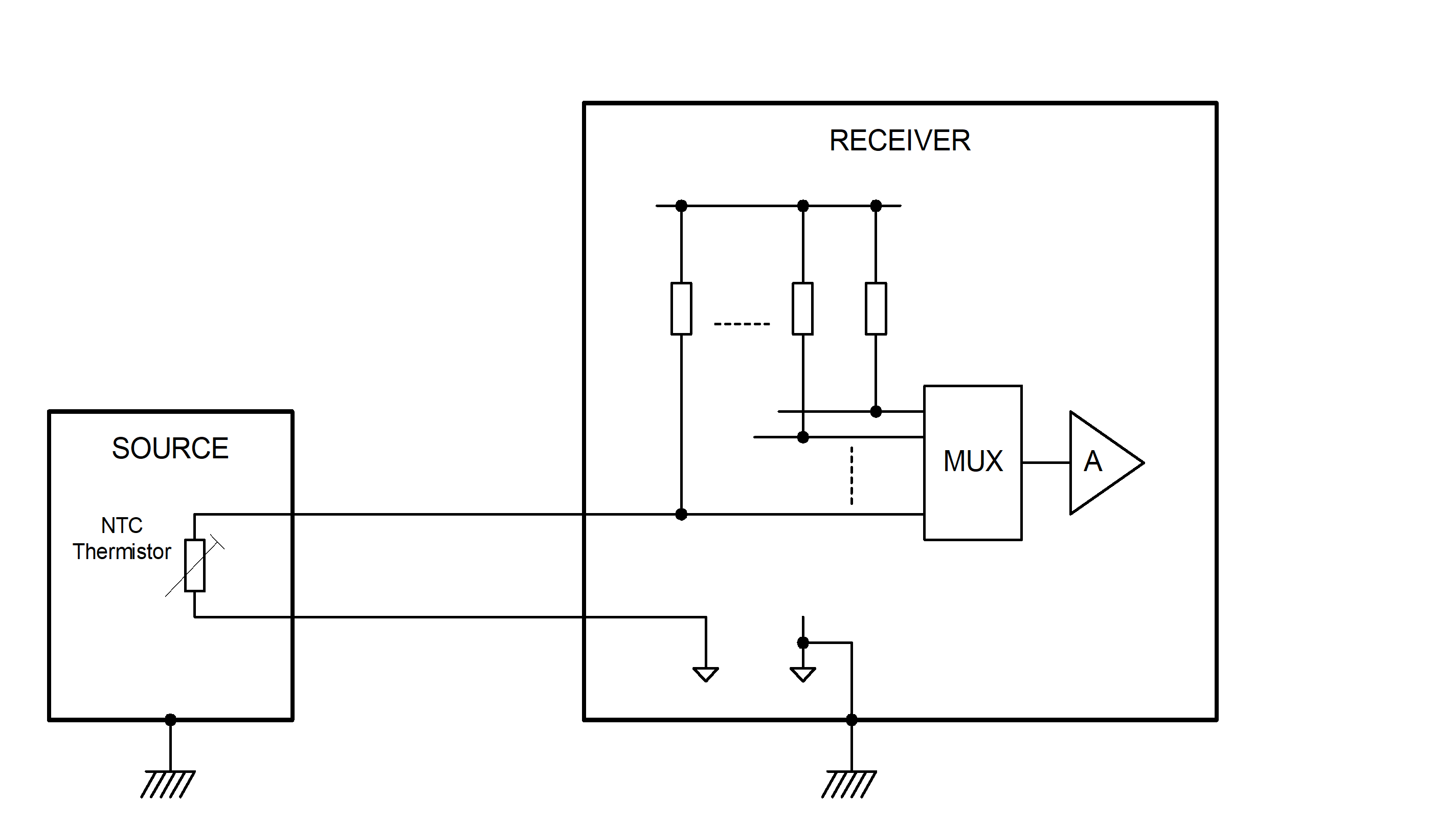 Figure 55: TSM1 interface arrangement
TSM2
Overview
The TSM2 interface has the following features:
The measurable resistance range is specified from 0 to up to RMAX.
RMAX can be seen as the maximum resistance of the thermistor in the temperature range of interest.
RMAX can be chosen as characteristic of a group of channels within a specific range.
The specified accuracy is expressed as a maximum error ±x.
The specified accuracy in terms of resistance is expressed as xRMAX.
The resistance accuracy is specified at the DHS unit terminals, i.e. excluding any error contribution from the thermistor or harness.
TSM2 error model
The maximum error in Rth, Rth, expressed as a function of x, shall be:
![]()
TSM2 source electrical characteristics
The source shall meet the characteristics specified in Table 55.
Table 55: TSM2 source characteristics
|
Reference
|
Characteristic
|
Value
|
|
5.3.5.2.3 a.1
|
Circuit type
|
Floating Resistive sensor
|
|
5.3.5.2.3 a.2
|
Transfer
|
DC coupled
|
|
5.3.5.2.3 a.3
|
Resistance range, Rs
|
0 Ω to RMAX
|
|
5.3.5.2.3 a.4
|
Fault voltage tolerance, Vsft
|
-17,5 V to +17,5 V with an overvoltage source impedance ≥ 1 kΩ
|
TSM2 receiver electrical characteristics
The receiver shall meet the characteristics specified in Table 56.
Table 56: TSM2 receiver characteristics
|
Reference
|
Characteristic
|
Value
|
|
5.3.5.2.4 a.1
|
Circuit type
|
Single ended receiver with multiplexed inputs
|
|
5.3.5.2.4 a.2
|
Transfer
|
DC coupled
|
|
5.3.5.2.4 a.3
|
Sensor injected power, Pi
|
≤ 1 mW
|
|
5.3.5.2.4 a.4
|
Measurement error, x
|
< ±0,01
|
|
5.3.5.2.4 a.5
|
Parameterized resistance range, RMAX
|
1 kΩ to 5 kΩ, to be specified per group of channels
|
|
5.3.5.2.4 a.6
|
Fault voltage emission, Vrfe
|
-16,5 V to +16,5 V with a source impedance of ≥ 1,0 kΩ
|
|
5.3.5.2.4 a.7
|
Fault tolerance, Rrft
|
Short circuit to ground
|
Harness
Wire type
The wire type shall be twisted n-tuple.
Core to core capacitance
The capacitance CCC measured between the two core wires shall be less than or equal to 1 nF.
Interface arrangement
The electrical interface arrangement is specified in Figure 56.
Circuitry is indicative only; other implementations meeting the above requirements are not excluded.
 Figure 56: TSM2 interface arrangement
TSM examples
TSM1 examples
All thermistors of NTC type show a quasi-exponential temperature sensitivity in Rth/Rth of roughly 4 %/C or one decade per 60 C. That means that when using an NTC thermistor for a TSM1 channel, Figure 54 can be used as a general indication of accuracy in temperature by:
rescaling the y-axis by a factor 1C/0,04,
exchanging the logarithmic x-axis with a linear temperature scale where minimum point of |Rth/Rth| is set to thermistor temperature at RNORM and one decade corresponds to 60C.
4K3A354 (ESCC Detail Specification No. 4006/013, variant 04) is a thermistor with nominally 4 k resistance at 25C. Figure 57 shows temperature accuracy specifically of a 4K3A354 thermistor connected to a TSM1 channel specified with RNORM = 4 k . The figure does not include any inaccuracy of the sensor itself
YSI44907 is a thermistor with nominally 10 k resistance at 25 C. Figure 58 shows temperature accuracy specifically of a YSI44907 thermistor connected to a TSM1 channel specified with RNORM = 10 k .
As shown in the two examples, the accuracy in terms of temperature becomes quite similar for different NTC thermistor types, provided that RNORM is selected per type for the same temperature range.
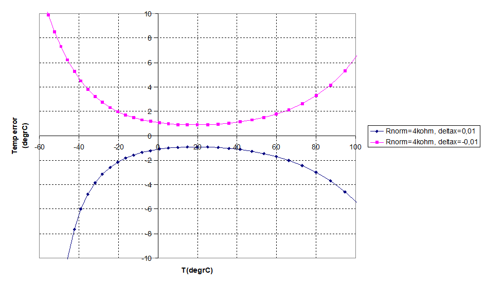 Figure 57: Example TSM1 and 4K3A354 thermistor
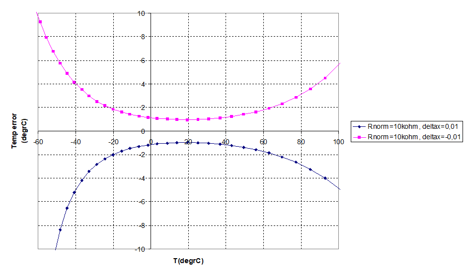 Figure 58: Example TSM1 and YSI44907 thermistor
TSM2, PT1000
The platinum temperature sensors show fairly constant temperature sensitivity in Rth of roughly 0.004R0/C, where R0 is the nominal resistance (at 0 C).
PT1000 is a platinum sensor with nominally 1000 resistance at 0 C. Figure 59 shows temperature accuracy specifically of a PT1000 connected to a TSM2 channel specified with RMAX = 1700 . The figure does not include any inaccuracy of the sensor itself.
RMAX = 1700 for the PT1000 sensor covers the temperature range up to +183 C.
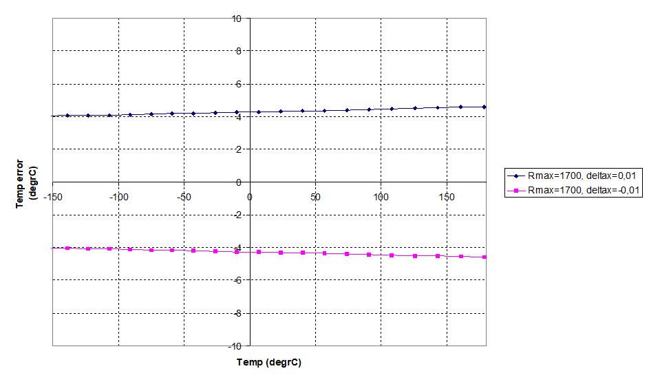 Figure 59: Example TSM2 and PT1000 thermistor
Bi-level discrete input interfaces
Bi-level discrete monitor (BDM) interface
Overview
The bi-level discrete monitor (BDM) interfaces are used for reasonably static, discrete status and telemetry monitoring by the core element. The monitored signal is bi-level discrete in that it can take only two values, high or low, indicated by the signal voltage.
The bi-level discrete interface consists of a signal, BL_DATA_IN, which is generated by the peripheral element. This signal is sampled periodically by the core element.
In a practical implementation, a number of bi-level discrete interfaces can be aggregated to form a multiple bit data word in the core element.
The bi-level discrete input interface consists of a signal, BL_DATA_IN, which can assume two values, high or low, with respect to the signal reference. This signal is maintained continuously by the peripheral element and can be sampled at any time by the core element.
On sampling, the core element encodes the BL_DATA_IN value into a single binary bit of data which can be embedded in a larger data word.
There are no timing parameters associated with this interface. The BL_DATA_IN signal is maintained continuously by the peripheral element and can generally be regarded as static. However, if the BL_DATA_IN signal is sampled during a transition from one level to the other, the result determined by the core element can be invalid.
Bi-level discrete monitor interface
Bi-level discrete monitor input interface - BL_DATA_IN signal
The peripheral element shall
- provide a BL_DATA_IN signal, and
- continually maintain such signal in one of two states, high (logical ‘1’) or low (logical ‘0’).
BDM electrical characteristics
Source circuit
The source circuit shall meet the characteristics specified in Table 61.
Table 61: BDM source characteristics
|
Reference
|
Characteristic
|
Value
|
|
6.1.2.2.1 a.1
|
Circuit type
|
Single ended
|
|
6.1.2.2.1 a.2
|
Transfer
|
DC coupled
|
|
6.1.2.2.1 a.3
|
Zero reference
|
Signal ground
|
|
6.1.2.2.1 a.4
|
Low output voltage, VLout
|
0 V to +0,5 V
|
|
6.1.2.2.1 a.5
|
High output voltage, VHout
|
2,4 V to +5,5 V,
|
|
6.1.2.2.1 a.6
|
Output impedance, Zout
|
5 k
|
|
6.1.2.2.1 a.7
|
Fault voltage emission, Vsfe
|
-1 V to +7 V
|
|
6.1.2.2.1 a.8
|
Fault voltage tolerance, Vsft
|
-17,5 V to +17,5 V with an overvoltage source impedance of 1,0 k
|
Receiver circuit
The receiver circuit shall meet the characteristics specified in Table 62.
Table 62: BDM receiver characteristics
|
Reference
|
Characteristic
|
Value
|
|
6.1.2.2.2 a.1
|
Circuit type
|
Differential receiver with multiplexed inputs
|
|
6.1.2.2.2 a.2
|
Transfer
|
DC coupled
|
|
6.1.2.2.2 a.3
|
Low level differential input voltage, VLin
|
0 V to 0,9 V
|
|
6.1.2.2.2 a.4
|
High level differential input voltage, VHin
|
2,0 V to 5,5 V
|
|
6.1.2.2.2 a.5
|
Ground displacement voltage, VGD
|
-1 V to 1 V up to 1 kHz rolling-off at 20 dB/decade up to 1 MHz
|
|
6.1.2.2.2 a.6
|
Input impedance, Zin
|
During acquisition: 100 k
|
|
6.1.2.2.2 a.7
|
Fault voltage emission, Vrfe
|
-16,5 V to +16,5 V with a series impedance of 1,0 k
|
|
6.1.2.2.2 a.8
|
Fault voltage tolerance, Vrft
|
-2 V to +8 V
|
Harness
Wire type
Both twisted pair and twisted shielded pair lines may be used.
Shields shall be connected to structure ground on source and receiver side.
Core to shield capacitance
If shielded pair is used, the capacitance CCS measured between the core wire and the shield shall be 2 nF.
Core to core capacitance
If unshielded pair is used, the capacitance CCC measured between the two core wires shall be 1 nF.
Interface arrangement
The electrical interface arrangement is depicted in Figure 61. The figure shows a specific implementation as example, but other implementations conforming to the requirements are not excluded.
 Figure 61: BDM Interface configuration
Bi-level switch monitor (BSM) interface
General principles
The bi-level switch monitor (BSM) interface is used by the core element to determine the status of a switch in the peripheral element. The peripheral element of this interface is entirely passive, consisting only of a single pole switch electrically isolated from all other components of the peripheral element.
This interface is used by the core element to determine the status of switches and relays in the peripheral element and has the advantage that it can be operated even when the peripheral element is powered down.
The switch status interface is entirely driven and operated by the core element. The core element provides a continuous reference voltage signal, and periodically samples the input signal and compares it to the reference. The result is encoded into a binary bit to indicate whether the switch was closed or open.
There are no timing constraints related to this interface since the switch status being monitored is normally static or changing infrequently. However, if the input signal is sampled while the switch status is changing, the result can be invalid.
The signal interface receiver is similar to a bi-level discrete (BDM) input with the following exceptions:
Ground is referred to receiver (instead of source) ground.
It is biased to a high level, when it is not being driven, by the connection of the input to a reference voltage through a resistance. When the switch contact is closed, the input signal is forced to a low level by presented low impedance.
The interface receiver converts such input signal in one of two digital states, high (logical ‘1’) for switch source open status, or low (logical ‘0’) for switch source closed status.
In case of specific needs, opto-couplers can be used. In that case the specific interfaces are defined on a system basis, thus they are not covered by this Standard.
Bi-level switch monitor interface
Source circuit
The source circuit shall meet the characteristics specified in Table 63.
Table 63: Switch source characteristics
|
Reference
|
Characteristic
|
Value
|
|
6.2.2.1 a.1
|
Circuit type
|
Floating Relay contact
|
|
6.2.2.1 a.2
|
Transfer
|
DC coupled
|
|
6.2.2.1 a.3
|
Operating current, Iop
|
Up to 10 mA
|
|
6.2.2.1 a.4
|
Operating voltage (open circuit), Vop
|
Up to 15 V
|
|
6.2.2.1 a.5
|
Switch closed resistance, RC
|
50
|
|
6.2.2.1 a.6
|
Switch open resistance, RO
|
1 M
|
|
6.2.2.1 a.7
|
Fault voltage tolerance, Vsft
|
-17,5 V to +17,5 V with an overvoltage source impedance of 1,0 k
|
Receiver circuit
The receiver circuit shall meet the characteristics specified in Table 64.
Table 64: Switch receiver characteristics
|
Reference
|
Characteristic
|
Value
|
|
6.2.2.2 a.1
|
Circuit Type
|
Single ended receiver with pull-up resistor
|
|
6.2.2.2 a.2
|
Transfer
|
DC coupled
|
|
6.2.2.2 a.3
|
Zero reference
|
Signal ground
|
|
6.2.2.2 a.4
|
Output current, Iout
|
0,1 mA to 10 mA (when contacts closed)
|
|
6.2.2.2 a.5
|
Output voltage, Vout
|
< 15 V (when contacts open)
|
|
6.2.2.2 a.6
|
Fault voltage emission, Vrfe
|
-16,5 V to +16,5 V with a source impedance of 1,0 k
|
|
6.2.2.2 a.7
|
Fault tolerance, Vrft
|
Short circuit to ground
|
Harness
Wire type
The wire type shall be twisted n–tuple type.
Core to core capacitance
The capacitance CCC measured between the two core wires shall be 1 nF.
Interface arrangement
The electrical interface arrangement is depicted in Figure 62, which shows specific implementation to be taken as example, but other implementations conforming to requirements are not excluded.
 Figure 62: Switch status circuit interface arrangement
Pulsed command interfaces
High power command (HPC) interfaces
General principles
The high power pulse (HPC) command interfaces are intended for load driving interfaces and, for example, can be used to switch relays or similar loads. The high current capabilities of these interfaces lead to their protection against short circuiting and against failure in a high current mode.
The high power pulse command consists of a single signal, HPC_OUT(H), generated by the core element. This is connected by a single ended circuit to the input at the peripheral element. The interface is entirely controlled from the core element.
Three classes of HPC are defined here:
LV-HPC : low voltage HPC (clause 7.1.3),
HV-HPC : high voltage HPC (clause 7.1.4), and
HC-HPC : high current HPC (clause 7.1.5).
High power command interface
High power pulse command - HPC_OUT(H) signal
The core element shall
- provide an HPC_OUT(H) signal, and
- drive such a signal.
High power pulse command - HPC_OUT(H) signal passive state
The passive state of the HPC_OUT(H) signal shall be low.
High power pulse command - HPC_OUT(H) signal active state
The active state of the HPC_OUT(H) signal shall be high.
High power pulse command output – driver unpowered
The HPC_OUT(H) output signal shall be in passive state when the driver is unpowered.
High power pulse command output - failure mode
The design of the high power pulse command interface shall ensure that no failure mode results in the output being permanently active (high state).
High power command configuration
The high power discrete pulse command source shall be referenced to source signal ground.
The load shall be isolated from any user electrical reference.
High power command transient protection
Both the high power pulse command source and receiver shall be equipped with circuits to suppress any switching transients.
This is particularly important to suppress transients due to inductive loads such as relays, which can cause the current drive capability, or the overvoltage capability of the source to be exceeded.
High power command short circuit protection
The high power pulse command source shall be short circuit proof for short circuits to source or receiver signal ground and structure.
Low voltage high power command (LV-HPC) electrical characteristics
Source circuit
The source circuit shall meet the characteristics specified in Table 71.
Table 71: LV-HPC source characteristics
|
Reference
|
Characteristics
|
Value
|
|
7.1.3.1 a.1
|
Circuit type
|
Single ended driver return over wire
|
|
7.1.3.1 a.2
|
Transfer
|
DC coupled
|
|
7.1.3.1 a.3
|
Active state output voltage, VAout
|
12 V to 16 V
|
|
7.1.3.1 a.4
|
Passive state output leakage current, IPout
|
< 100 µA
|
|
7.1.3.1 a.5
|
Pulse width, tP
|
4 ms to 1024 ms (system design selectable depending on receiver characteristics)
|
|
7.1.3.1 a.6
|
Output voltage rise and fall times, tr, tf
|
50 µs to 2 ms when connected to a resistive load of 100
|
|
7.1.3.1 a.7
|
Active current drive capability, IAout
|
180 mA
|
|
7.1.3.1 a.8
|
Free-wheeling current capability (in Passive state)
|
IAout during tP
|
|
7.1.3.1 a.9
|
Short circuit output current, ISC
|
400 mA
|
|
7.1.3.1 a.10
|
Fault voltage tolerance, Vsft
|
0 V to +20 V
|
|
7.1.3.1 a.11
|
Fault voltage emission, Vsfe
|
0 V to +19 V
|
Receiver circuit
The receiver circuit shall meet the characteristics specified in Table 72.
Table 72: LV-HPC receiver characteristics
|
Reference
|
Characteristics
|
Value
|
|
7.1.3.2.a.1
|
Circuit type
|
Relay or opto-coupler
|
|
7.1.3.2 a.2
|
Transfer
|
DC coupled
|
|
7.1.3.2 a.3
|
Active level at unit input terminal, VAin
|
11 V to 16 V
|
|
7.1.3.2 a.4
|
Passive current at unit input terminal (no activation), IPin
|
200 µA
|
|
7.1.3.2 a.5
|
Passive level transient immunity, tPtran
|
No activation for pulses up to the active level 100 s wide
|
|
7.1.3.2 a.6
|
Load current, Iload
|
180 mA (at 16 V)
|
|
7.1.3.2 a.7
|
Inputs to chassis isolation, Ziso
|
> 1 M
|
|
7.1.3.2 a.8
|
Fault voltage emission, Vrfe
|
0 V to +19 V
|
|
7.1.3.2 a.9
|
Fault voltage tolerance, Vrft
|
0 V to +20 V
|
High voltage high power command (HV-HPC) electrical characteristics
HV-HPC source circuit
The HV-HPC source circuit shall meet the characteristics specified in Table 73.
Table 73: HV-HPC source characteristics
|
Reference
|
Characteristic
|
Value
|
|
7.1.4.1 a.1
|
Circuit type
|
Single ended driver return over wire
|
|
7.1.4.1 a.2
|
Transfer
|
DC coupled
|
|
7.1.4.1 a.3
|
Active state output voltage, VAout
|
22 V to 29 V
|
|
7.1.4.1 a.4
|
Passive state output leakage current, IPout
|
< 100 µA
|
|
7.1.4.1 a.5
|
Pulse width, tP
|
4 ms to 1024 ms (system design selectable depending on receiver characteristics)
|
|
7.1.4.1 a.6
|
Output voltage rise and fall times, tr, tf
|
50 µs to 2 ms when connected to a resistive load of 200
|
|
7.1.4.1 a.7
|
Active current drive capability, IAout
|
180 mA
|
|
7.1.4.1 a.8
|
Free-wheeling current capability (in passive state)
|
IAout during tP
|
|
7.1.4.1 a.9
|
Short circuit output current, ISC
|
400 mA
|
|
7.1.4.1 a.10
|
Fault voltage tolerance, Vsft
|
0 V to +33 V
|
|
7.1.4.1 a.11
|
Fault voltage emission, Vsfe
|
0 V to +32 V
|
HV-HPC receiver circuit
The HV-HPC receiver circuit shall meet the characteristics specified in Table 74.
Table 74: HV-HPC receiver characteristics
|
Reference
|
Characteristic
|
Value
|
|
7.1.4.2 a.1
|
Circuit type
|
Relay or opto-coupler
|
|
7.1.4.2 a.2
|
Transfer
|
DC coupled
|
|
7.1.4.2 a.3
|
Active level at unit input terminal, VAin
|
21 V to 29 V
|
|
7.1.4.2 a.4
|
Passive current at unit input terminal (no activation), IPin
|
200 µA
|
|
7.1.4.2 a.5
|
Passive level transient immunity, tPtran
|
No activation for pulses up to the active level 100 s wide
|
|
7.1.4.2 a.6
|
Load current, Iload
|
180 mA (at 29 V)
|
|
7.1.4.2 a.7
|
Inputs to chassis isolation, Ziso
|
> 1 M
|
|
7.1.4.2 a.8
|
Fault voltage emission, Vrfe
|
0 V to +32 V
|
|
7.1.4.2 a.9
|
Fault voltage tolerance, Vrft
|
0 V to +33 V
|
High current high power command (HC-HPC) electrical characteristics
HC-HPC source circuit
The HC-HPC source circuit shall meet the characteristics specified in Table 75.
Table 75: HC-HPC source characteristics
|
Reference
|
Characteristic
|
Value
|
|
7.1.5.1 a.1
|
Circuit type
|
Single ended driver return over wire
|
|
7.1.5.1 a.2
|
Transfer
|
DC coupled
|
|
7.1.5.1 a.3
|
Active state output voltage, VAout
|
22 V to 29 V
|
|
7.1.5.1 a.4
|
Passive state output leakage current, IPout
|
< 1 mA
|
|
7.1.5.1 a.5
|
Pulse width, tP
|
4 ms to 1024 ms (system design selectable depending on receiver characteristics)
|
|
7.1.5.1 a.6
|
Output voltage rise and fall times, tr, tf
|
50 µs to 2 ms when connected to a resistive load of 50
|
|
7.1.5.1 a.7
|
Active current drive capability, IAout
|
600 mA
|
|
7.1.5.1 a.8
|
Free-wheeling current capability (in passive state)
|
IAout during tP
|
|
7.1.5.1 a.9
|
Short circuit output current, ISC
|
1 A
|
|
7.1.5.1 a.10
|
Fault voltage tolerance, Vsft
|
0 V to +33 V
|
|
7.1.5.1 a.11
|
Fault voltage emission, Vsfe
|
0 V to +32 V
|
HC-HPC receiver circuit
The HC-HPC receiver circuit shall meet the characteristics specified in Table 76.
Table 76: HC-HPC receiver characteristics
|
Reference
|
Characteristic
|
Value
|
|
7.1.5.2 a.1
|
Circuit type
|
Relay
|
|
7.1.5.2 a.2
|
Transfer
|
DC coupled
|
|
7.1.5.2 a.3
|
Active level at unit input terminal, VAin
|
20 V to 29 V
|
|
7.1.5.2 a.4
|
Passive level at unit input terminal (no activation), IPin
|
2 mA
|
|
7.1.5.2 a.5
|
Passive level transient immunity, tPtran
|
No activation for pulses up to the active level 1 ms wide
|
|
7.1.5.2 a.6
|
Load current, Iload
|
600 mA (at 29 V)
|
|
7.1.5.2 a.7
|
Inputs to chassis isolation, Ziso
|
> 1 M
|
|
7.1.5.2 a.8
|
Fault voltage emission, Vrfe
|
0 V to +32 V
|
|
7.1.5.2 a.8
|
Fault voltage tolerance, Vrft
|
0 V to +33 V
|
Wiring type
Both twisted n-tuples and twisted shielded n-tuples lines may be used.
Shield shall be connected to structure ground on source and receiver side.
High power command interface arrangement
The interface arrangement is presented in Figure 71, which shows a specific implementation taken as an example, but other implementations conforming to requirements are not excluded.
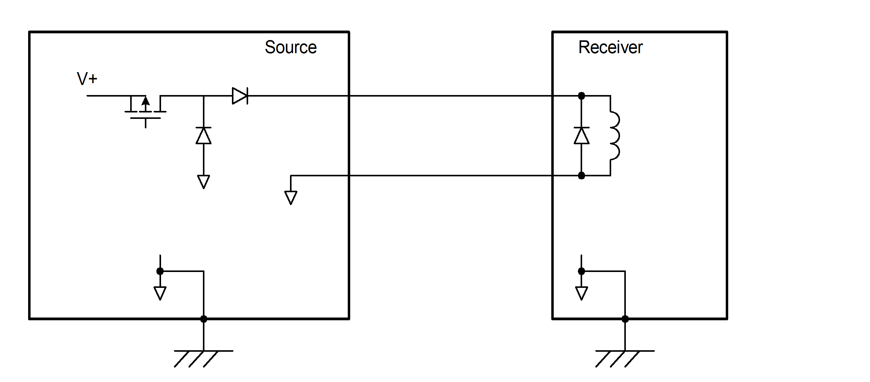 Figure 71: HPC interface arrangement
Low power command (LPC) interface
General
The low power (LPC) command interfaces are intended for driving opto-coupler channels.
Two types of opto-coupler interfaces are considered namely the opto-coupler pulse interface, LPC-P, and the opto-coupler static bi-level interface, LPC-S.
The low power command consists of a single signal, LPC_OUT(H), generated by the core element. This is connected by a single ended circuit to the input at the peripheral element. The interface is entirely controlled from the core element.
Low power command interface
Low power command - LPC_OUT(H) signal
The core element shall
- provide an LPC_OUT(H) signal, and
- drive such a signal.
Low power command - LPC_OUT(H) signal passive state
The passive state of the LPC_OUT(H) signal shall be low.
Low power command - LPC_OUT(H) signal active state
The active state of the LPC_OUT(H) signal shall be high.
Low power command output – driver unpowered
The LPC_OUT(H) output signal shall be in passive state when the driver is unpowered.
Low power command configuration
The low power discrete pulse command source shall be referenced to source signal ground.
The load shall be isolated from any user electrical reference.
Low power command short circuit protection
The low power pulse command source shall be short circuit proof for short circuits to source or receiver signal ground and structure.
LPC electrical characteristics
Source circuit
The source circuit shall meet the characteristics specified in Figure 72 and Table 77.
Figure 72 shows the LPC source high level output voltage vs. load current. A typical load is indicated as a dashed line.
Table 77: LPC source characteristics
|
Reference
|
Characteristics
|
Value
|
|
7.2.3.1 a.1
|
Circuit type
|
Single ended driver return over wire
|
|
7.2.3.1 a.2
|
Transfer
|
DC coupled
|
|
7.2.3.1 a.3
|
Output resistance, Rout
|
370 to 430
|
|
7.2.3.1 a.4
|
Active signal open circuit output voltage, VAout
|
4,4 V to 5,5 V
|
|
7.2.3.1 a.5
|
Passive signal open circuit output voltage, VPout
|
0 V to 0,5 V
|
|
7.2.3.1 a.6
|
Fault voltage emission, Vsfe
|
7 V with a source impedance 350
|
|
7.2.3.1 a.7
|
Fault tolerance
|
Continuous short circuit
|
|
7.2.3.1 a.8
|
Pulse width for LPC-P
|
4 ms ≤ td ≤ 120 ms
|
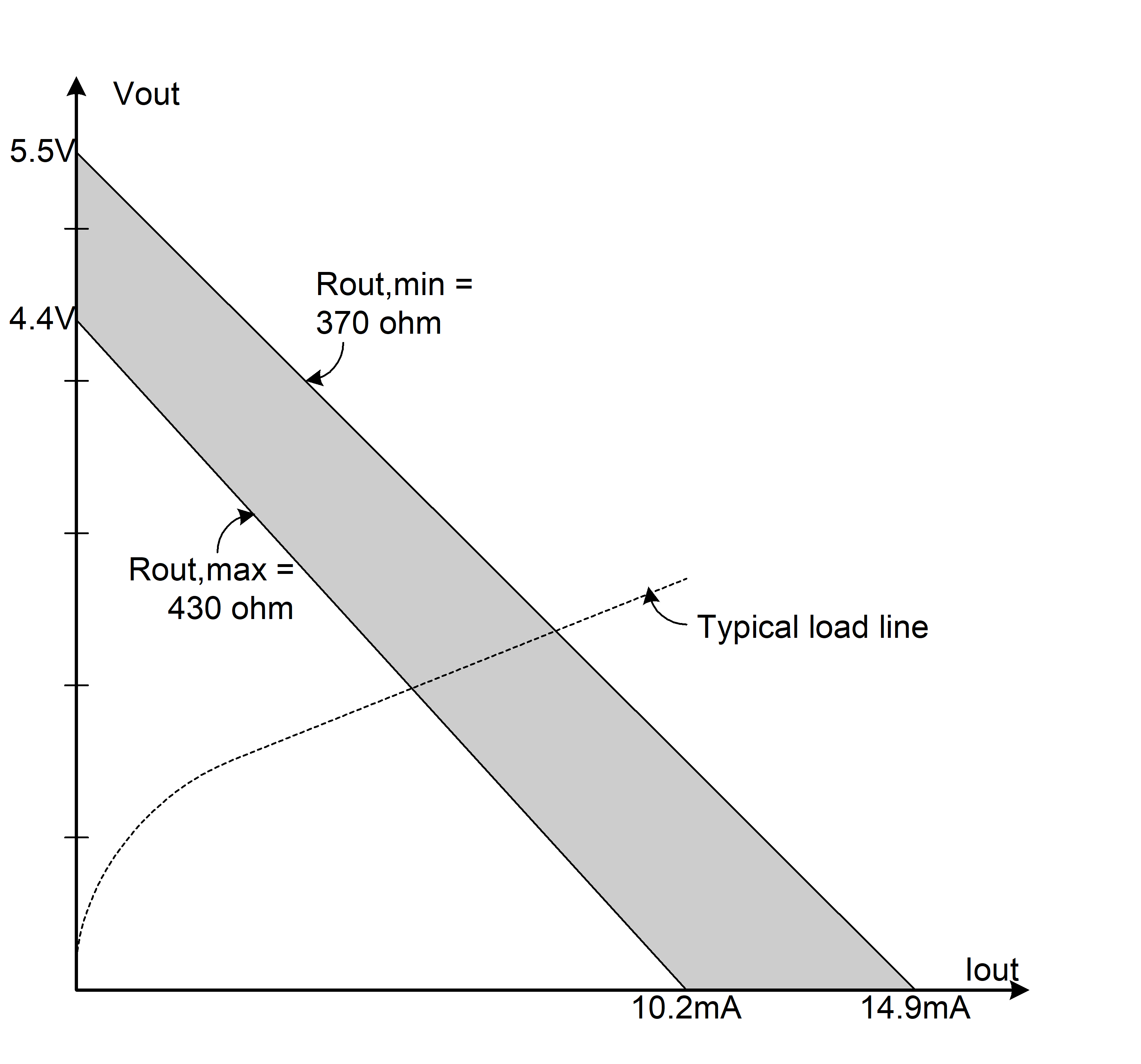 Figure 72: LPC active signal output voltage vs. load current
Receiver circuit
The receiver circuit shall meet the characteristics specified in Table 78.
Table 78: LPC receiver characteristics
|
Reference
|
Characteristics
|
Value
|
|
7.2.3.2 a
|
Circuit type
|
Opto-coupler, passive load
|
|
7.2.3.2 b
|
Transfer
|
DC coupled
|
|
7.2.3.2 c
|
Active input signal, VAin
|
4,4 V to 5,5 V through a 370 Ω to 450 Ω source resistance
|
|
7.2.3.2 d
|
Passive input signal, VPin
|
0 V to 0,5 V
|
|
7.2.3.2 e
|
Fault voltage tolerance, Vrft
|
7 V with a source impedance of 350
|
|
7.2.3.2 f
|
Input to chassis isolation, Ziso
|
>1 MΩ
|
Wiring type
Both twisted n-tuples and twisted shielded n-tuples lines may be used.
Shield shall be connected to structure ground on source and receiver side.
Interface arrangement
The scheme depicted in Figure 73 is applicable to both LPC-P and LPC-S. The figure shows a specific implementation taken as an example, but other implementations compliant to requirements are not excluded.
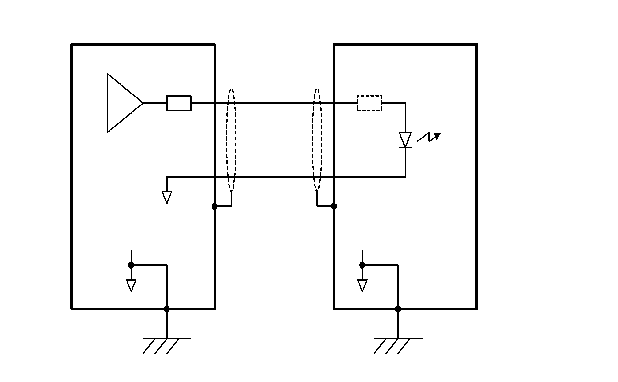 Figure 73: LPC-P and LPC-S interface arrangement
Serial digital interfaces
Foreword
This clause refers to the implementation of 16-bit serial digital point to point interfaces as specified in clause 8.2.
Other serial digital point to point interfaces may be used in space applications. They are not covered by this Standard. However, all digital interfaces referencing RS-422 as the physical layer (e.g. synchronization pulses) are recommended to comply with this specification for electrical characteristics as in clause 8.8.
General principles of serial digital interfaces
Overview
The serial digital interfaces are used to exchange digital data words between core and peripheral elements. The interface timing and clocking signals are controlled by the core element.
A serial digital interface which reads data from the peripheral element into the core element is called an input serial digital (ISD) interface. A serial digital interface which writes data out from the core element to the peripheral element is called an output serial digital (OSD) interface. A third class of serial digital interface is also introduced in this standard, namely the bi-directional serial digital (BSD) interface.
For space applications, serial digital interfaces shall be implemented in balanced differential form. In this form each signal is carried by a pair of conductors and the level of the signal is determined by the differential voltage between those conductors.
The serial digital interfaces are based on five signals, namely:
GATE_WRITE provided by the core element which indicates when a write transfer (from core to peripheral) is underway,
GATE_READ provided by the core element which indicates when a read transfer (from peripheral to core) is underway,
DATA_CLK_OUT provided by the core element which controls the data transfer timing,
DATA_OUT provided by the core element in the case of output and bi-directional interfaces, and
DATA_IN provided by the peripheral element in the case of input and bi-directional interfaces.
In a practical implementation, the DATA_CLK_OUT and, for output interfaces, the DATA_OUT signal can be distributed to several devices. However, each device has its own unique GATE_WRITE (READ) signal.
Signals in Figure 82 and Figure 84 indicate the expected TRUE line waveform of the differential interface. DATA_OUT and DATA_IN low denotes a logic ‘0’ and the corresponding HIGH denotes a logic ‘1’.
The serial interface timing in this standard is specified in proportion to the bit period (tb), which is implementation dependent: once it is specified by the designer, the other characteristics are defined as a function of tb.
As specified in 8.2.2, it is important that the peripheral element is designed to be compatible with any tb specified in this Standard.
In addition the standard provides some recommended implementation options.
These interfaces correspond to the 16-bit digital channel telemetry interfaces and the 16-bit memory load commands described in TTC-B-01 but with some modifications. Most significantly, none of these word exchanges need be aligned with the OBDH bus interrogation slot interval.
- 1 This is a relaxation of requirements and is in line with the philosophy of supporting systems which use MIL-STD-1553B instead of the ESA OBDH bus.
- 2 Where an ESA OBDH bus is being used, this standard does not preclude synchronisation with the interrogation slot intervals, but does not specify its use.
- 3 16-bit transfers are now preferably performed in a single burst rather than in two 8-bit.
General requirements
The physical layer of serial digital interfaces shall conform to the requirements in ANSI/TIA/EIA-422 and those specified in this clause 8 of this Standard.
The peripheral element should be designed to be compatible with any tb specified in 8.3.4.8 and 8.4.4.9.
16-bit input serial digital (ISD) interface
16-bit input serial digital interface description
The signal arrangement for the 16-bit input serial digital interface is shown in Figure 82.
The 16-bit input serial digital interface consists of three signals, namely GATE_READ, DATA_CLK_OUT, and DATA_IN. The GATE_READ and DATA_CLK_OUT are used to control the operation of the interface and are driven by the core element. The DATA_IN signal is used to carry the data to be transferred and is driven by the peripheral element.
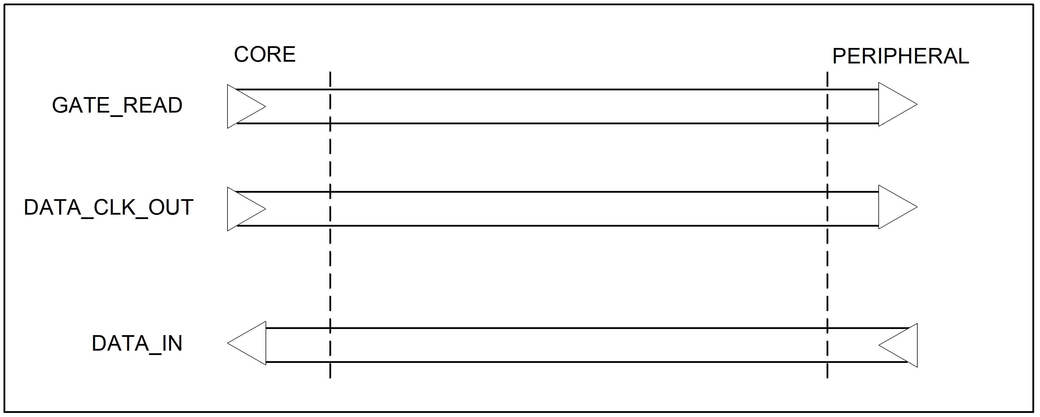 Figure 81: 16-bit input serial digital (ISD) interface signal arrangement
Signals skew
Introduction
In the values listed in Table 81 a skew is considered between any pair of signals or subsequent edges of the same signal to account for components characteristics and/or harness routing asymmetry.
Provisions
Maximum skew measured at core side shall be t = 0,02 × tb .
Maximum skew measured at peripheral side shall be t = 0,04 × tb .
ISD interface timing specification
The timing diagram shown in Figure 82 and the timing parameters in Table 81 specify the signal timing of the operational requirements specified in 8.3.4 for the 16-bit input serial digital interface.
A data transfer is initiated by the core element asserting GATE_READ. In response to this the peripheral element places the value of the most significant bit (bit 0) of the data word on the DATA_IN line.
After the GATE_READ falling edge (tcd), the core element generates a sequence of sixteen low going pulses out onto the DATA_CLK_OUT line. The core element samples the DATA_IN line on the falling edge of each DATA_CLK_OUT pulse. This same falling edge causes the peripheral element to output the next bit of the data word on the DATA_IN line.
The DATA_IN line state is not sampled after the last DATA_CLK_OUT falling edge and can return to its quiescent 'don't care' state.
Sometime after the last DATA_CLK_OUT falling edge the core element de-asserts the GATE_READ signal indicating the end of the data transfer (tgd).
GATE_READUP can occur at the same time, or even slightly before, the last DATA_CLK_OUTUP. The GATE_READ signal is subsequently kept de-asserted for a short period (trec) to enable the peripheral element to recover ready for the next data transfer.
 Figure 82: 16-bit input serial digital (ISD) interface
Table 81: 16-bit input serial digital (ISD) interface characteristics
|
Reference
|
Parameter
|
Description
|
Maximum
|
Minimum
|
|
8.3.3 a.1
|
tb
|
Bit sampling interval
|
tb (MAX)
|
tb (MIN)
|
|
8.3.3 a.2
|
ts
|
Repeated transfer period a
|
|
tb 17
|
|
8.3.3 a.3.(a)
|
tb0
|
GATE_READDOWN to bit 0 data valid, measured at peripheral element
|
tb 0,2
|
-
|
|
8.3.3 a.3.(b)
|
GATE_ READDOWN to bit 0 data valid, measured at core element
|
tb 0,3
|
-
| |
|
8.3.3 a.4
|
tcd
|
Clock delay, GATE_ READDOWN to first DATA_CLK_OUTDOWN
|
tb 7 + t
|
tb/2 – t
|
|
8.3.3 a.5
|
tdh
|
Data hold after DATA_CLK_OUTDOWN
|
-
|
0
|
|
8.3.3 a.6.(a)
|
tdv
|
Next data valid after DATA_CLK_OUTDOWN, measured at peripheral element
|
tb 0,7
|
-
|
|
8.3.3 a.6.(b)
|
Next data valid after DATA_CLK_OUTDOWN, measured at core element
|
tb 0,8
|
-
| |
|
8.3.3 a.7.(a)
|
tch
|
Time DATA_CLK_OUT high (clock duty cycle) measured at core element
|
tb/2 1,1
|
tb/2 0,9
|
|
8.3.3 a.7.(b)
|
Time DATA_CLK_OUT high (clock duty cycle) measured at peripheral element
|
tb/2 1,2
|
tb/2 0,8
| |
|
8.3.3 a.8
|
tgd
|
Gating delay, last DATA_CLK_OUT DOWN to GATE_READUP
|
tb 4 + t
|
tb/2 – t
|
|
8.3.3 a.9
|
trec
|
Recovery interval, GATE_READUP to GATE_READ DOWN
|
|
tb – t
|
|
8.3.3 a.10
|
tb8
|
Extension of gap b between clock pulse 8 and 9
|
tb × 8
|
0
|
|
a The transfer period is calculated as follows: ts = tcd + tgd + trec + 15·tb
| ||||
16-bit input serial digital interface: signal description
16-bit input serial digital - signals
The 16-bit input serial digital interface shall consist of three signals named GATE_READ, DATA_CLK_OUT, and DATA_IN.
- 1 GATE_READ and DATA_CLK_OUT are active low signals.
- 2 Signals are differential signals.
16-bit input serial digital - GATE_READ signal quiescent state
During quiescence, i.e. when no data transfer is taking place, the GATE_READ signal shall be maintained at a high logic level by the core element.
16-bit input serial digital - DATA_CLK_OUT signal
The DATA_CLK_OUT signal shall comprise sixteen low going pulses during each data transfer operation.
The DATA_CLK_OUT burst shall last 16 times the bit sampling pseudoperiod (tb) plus the optional extension of the clock gap between clock pulse 8 and 9 (tb8).
16-bit input serial digital - DATA_CLK_OUT signal quiescent state
Peripheral elements shall ignore the DATA_CLK_OUT signal when the GATE_READ signal is not asserted.
The reason is that during quiescence, i.e. when no data transfer is taking place, the DATA_CLK_OUT signal can oscillate (e.g. if it is shared with other peripheral elements).
16-bit input serial digital - DATA_IN signal
The peripheral element shall provide a DATA_IN signal.
The peripheral element shall ensure that the data on this signal is valid and stable on every DATA_CLK_OUT falling edge when GATE_READ is asserted.
16-bit input serial digital - DATA_IN signal quiescent state
During quiescence, the core element shall disregard the DATA_IN signal.
Peripheral element should maintain the DATA_IN signal in a stable state.
The actual level used by the peripheral element is not mandated.
16-bit input serial digital - data transfer
Data transfer on the 16-bit ISD shall be started by the core element, asserting the GATE_READ signal.
In response to the GATE_READDOWN the peripheral element shall set the DATA_IN signal to the value of the most significant bit, bit 0, of the data word.
The core element shall then sample the DATA_IN signal on each falling edge of the DATA_CLK_OUT (DATA_CLK_OUTDOWN ).
After each DATA_CLK_OUT falling edge (DATA_CLK_OUTDOWN ), the peripheral element shall set the value of the DATA_IN signal to the value of the next most significant bit.
That means that if the current value of DATA_IN is bit n, the new value of DATA_IN is bit n+1.
When the 8th clock pulse on DATA_CLK_OUT has been generated, the gap to the next clock pulse may be increased by up to tb × 8.
When bit 15 of DATA_IN is reached, DATA_IN may be set to any value;
The reason is that the next value of DATA_IN is not important since the DATA_IN signal is not sampled after this.
16-bit input serial digital - bit sampling interval, tb
The bit sampling interval, tb, i.e. the interval between successive DATA_CLK_OUT rising edges, should be selected from the options shown in Table 82.
Table 82: tb values
|
Reference
|
tb (MIN)
|
tb (MAX)
|
Maximum sustainable data rate (Kbps)
|
|
8.3.4.8 a
|
7,95 s
|
8,05 s
|
118,387
|
|
8.3.4.8 b
|
7,59 s
|
7,67 s
|
124,002
|
|
8.3.4.8 c
|
3,95 s
|
4,05 s
|
238,273
|
|
8.3.4.8 d
|
3,78 s
|
3,85 s
|
248,988
|
16-bit input serial digital - sampling period, ts
The sampling period, ts, defined as the minimum period between one GATE_READDOWN and the next opportunity for a GATE_READDOWN, shall be not less than tb 17.
The transfer period is calculated as follows: ts = tcd + tgd + trec + 15∙tb.
16-bit input serial digital - data hold after DATA_CLK_OUTUP, tdh
The data hold time after the DATA_CLK_OUT falling edge, tdh, shall be not less than 0.
This ensures that the propagation delay always gives enough margin to hold the data.
16-bit output serial digital (OSD) interface description
16-bit output serial digital interface description
The signal arrangement for the 16-bit output serial digital interface is shown in Figure 82. Unless otherwise specified, signal properties are measured at the core interface.
The 16-bit output serial digital interface consists of three signals, namely GATE_WRITE, DATA_CLK_OUT, and DATA_OUT. All of three these signals are driven by the core element. The GATE_WRITE and DATA_CLK_OUT are used to control the operation of the interface and the DATA_OUT signal is used to carry the data to be transferred.
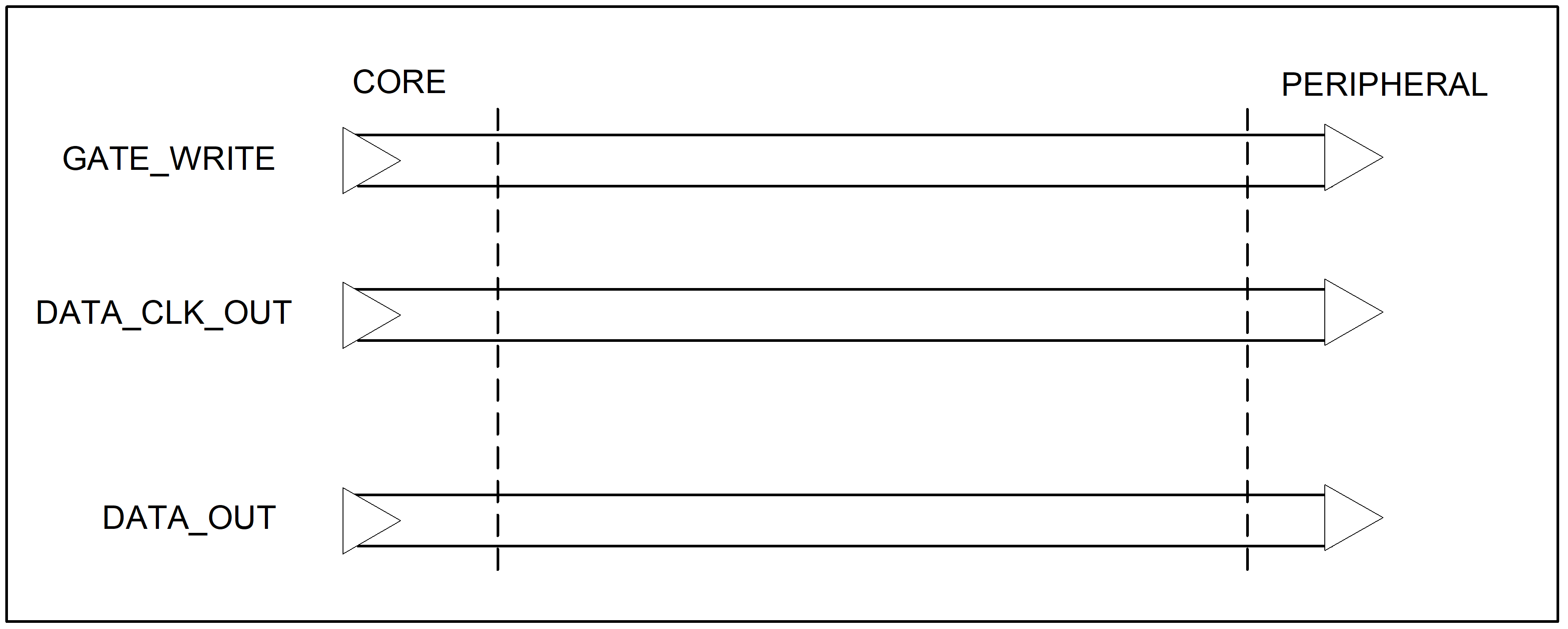 Figure 83: 16-bit output serial digital (OSD) interface signal arrangement
Signals skew
Overview
In the values listed in Table 83 a skew is considered between any pair of signals or subsequent edges of the same signal to account for component characteristics and/or harness routing asymmetry.
Provisions
Maximum skew measured at core side shall be t = 0,02 × tb .
Maximum skew measured at peripheral side shall be t = 0,04 × tb .
OSD interface timing specification
The timing diagram shown in Figure 84 and the timing parameters in Table 83 specify the timing of the operational requirements specified in 8.4.4 for the 16-bit output serial digital interface.
A data transfer is started by the core element asserting the GATE_WRITE signal to indicate that a data transfer is underway. After this (tb0) the core element places the value of the most significant data bit (bit 0) on the DATA_OUT line.
Some time after the GATE_WRITEDOWN, 16 low going pulses are output on the DATA_CLK_OUT signal. Each bit of the data word, including bit-0 is guaranteed valid on the DATA_CLK_OUT falling edge and for a given period before, data set up time tsu, and after it, data hold time tdh.
GATE_WRITE is de-asserted after the last GATE_CLK_OUTDOWN. This de-assertion can thus occur before the final GATE_CLK_OUTUP. GATE_WRITE then is not reasserted before the interface recovery period has expired.
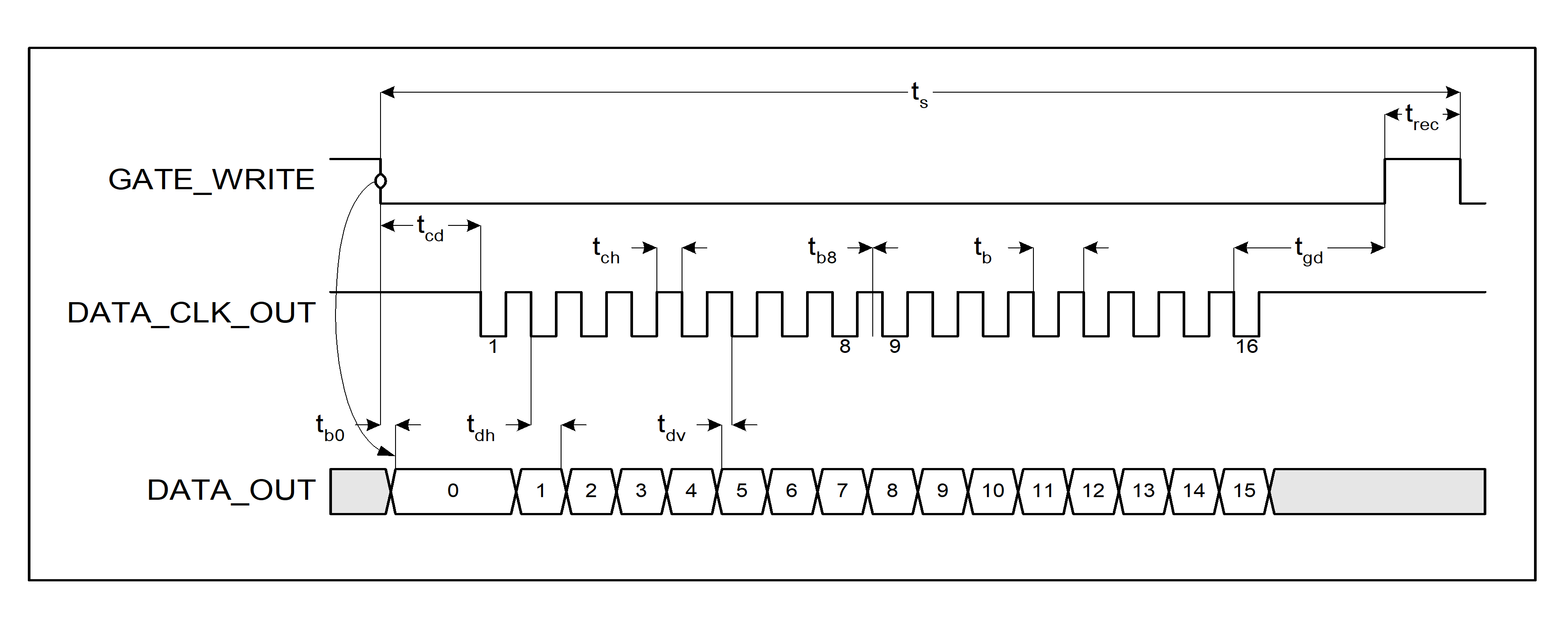 Figure 84: 16-bit output serial digital (OSD) interface
Table 83: 16-bit output serial digital (OSD) interface characteristics
|
Reference
|
Parameter
|
Description
|
Maximum
|
Minimum
|
|
8.4.1 a.1
|
tb
|
Bit sampling interval
|
tb (MAX)
|
tb (MIN)
|
|
8.4.1 a.2
|
ts
|
Repeated transfer period a
|
|
tb 17
|
|
8.4.1 a.3
|
tb0
|
Bit 0 data valid after GATE_WRITEDOWN
|
tb/4
|
-
|
|
8.4.1 a.4
|
tcd
|
Clock delay, GATE_WRITEDOWN to first DATA_CLK_OUTDOWN
|
tb 7 + t
|
tb/2 – t
|
|
8.4.1 a.5
|
tdh
|
Data hold after DATA_CLK_OUTDOWN
|
-
|
tb/8 – t
|
|
8.4.1 a.6
|
tsu
|
Data valid before DATA_CLK_OUTDOWN
|
-
|
tb/4 – t
|
|
8.4.1 a.7.(a)
|
tch
|
Time DATA_CLK_OUT high (clock duty cycle) measured at core element
|
tb/2 1,1
|
tb/2 0,9
|
|
8.4.1 a.7.(b)
|
Time DATA_CLK_OUT high (clock duty cycle) measured at peripheral element
|
tb/2 1,2
|
tb/2 0,8
| |
|
8.4.1 a.8
|
tgd
|
Gating delay, last DATA_CLK_OUTDOWN to GATE_WRITEUP
|
tb 4 + t
|
tb/2 – t
|
|
8.4.1 a.9
|
trec
|
Recovery interval, GATE_WRITEUP to GATE_WRITEDOWN
|
|
tb – t
|
|
8.4.1 a.10
|
tb8
|
Extension of gap b between clock pulse 8 and 9
|
tb 8
|
0
|
|
a The transfer period is calculated as follows: ts = tcd + tgd + trec + 15·tb
| ||||
16-bit output serial digital interface signal description
16-bit output serial digital - signals
The 16-bit output serial digital interface shall consist of three signals named GATE_WRITE, DATA_CLK_OUT, and DATA_OUT.
Signals shall be differential.
16-bit output serial digital - GATE_WRITE signal
The core element shall provide a GATE_WRITE signal asserted by the core element during a data transfer operation.
16-bit output serial digital - GATE_WRITE signal quiescent state
During quiescence, i.e. when no data transfer is taking place, the GATE_WRITE signal shall be maintained at a high logic level by the core element.
16-bit output serial digital - DATA_CLK_OUT signal
The core element shall provide a DATA_CLK_OUT signal.
The DATA_CLK_OUT signal shall comprise sixteen low going pulses during each data transfer operation.
The DATA_CLK_OUT burst shall last 16 times the bit sampling pseudoperiod (tb) plus the optional extension of the clock gap between clock pulses 8 and 9 (tb8).
16-bit output serial digital - DATA_CLK_OUT signal quiescent state
Peripheral elements shall ignore the DATA_CLK_OUT signal when the GATE_WRITE signal is not asserted.
The reason is that during quiescence, i.e. when no data transfer is taking place, the DATA_CLK_OUT signal can oscillate (e.g. if it is shared with other peripheral elements).
16-bit output serial digital - DATA_OUT signal
The core element shall provide a DATA_OUT signal used to transfer the data word bit serially.
16-bit output serial digital - DATA_OUT signal quiescent state
Peripheral elements shall ignore the DATA_OUT signal when the GATE_WRITE signal is not asserted.
The reason is that during quiescence, i.e. when no data transfer is taking place, the DATA_OUT signal can change (e.g. if it is shared with other peripheral elements).
16-bit output serial digital - data transfer
Data transfer on the 16-bit OSD shall be started by the core element, asserting the GATE_WRITE signal.
Shortly after the GATE_WRITEDOWN the core element shall set the DATA_OUT signal to the value of the most significant bit, bit 0, of the data word to be transferred.
The core element shall ensure that the DATA_OUT signal is valid on each falling edge of the DATA_CLK_OUT (DATA_CLK_OUTDOWN) when GATE_WRITE is asserted.
The DATA_OUT signal shall meet the data set-up and hold times as specified in Table 83.
Shortly after (after tdh) each DATA_CLK_OUT falling edge (DATA_CLK_OUTDOWN), the core element shall update the value of the DATA_OUT signal to the value of the next most significant bit.
That means that if the current value of DATA_OUT is bit n, the new value of DATA_OUT is bit n+1.
When the 8th clock pulse on DATA_CLK_OUT has been generated, the gap to the next clock pulse may be increased by up to tb × 8.
When bit 15 of DATA_IN is reached, any value may be used;
The reason is that the next value of DATA_OUT is not important since the peripheral element does not sample the DATA_OUT signal after this.
16-bit output serial digital - bit sampling interval, tb
The bit sampling interval, tb, i.e. the interval between successive DATA_CLK_OUT rising edges, should be selected from the options shown in Table 82.
16-bit output serial digital - sampling period, ts
The sampling period, ts, defined as the minimum period between one GATE_WRITEDOWN and the next opportunity for a GATE_WRITEDOWN, shall be not less than tb 17.
The transfer period is calculated as follows: ts = tcd + tgd + trec + 15∙tb.
16-bit bi-directional serial digital (BSD) interface description
The 16-bit bi-directional serial digital interface provides a bi-directional serial digital data transfer capability using five signals as shown in Figure 85:
GATE_WRITE,
GATE_READ,
DATA_CLK_OUT,
DATA_OUT, and
DATA_IN.
The GATE_WRITE and GATE_READ signals are used to indicate the direction of the transfer. The signal timing during output transfers is identical to that for the 16-bit output serial digital interface and during input transfers it is identical to the 16-bit input serial digital interface.
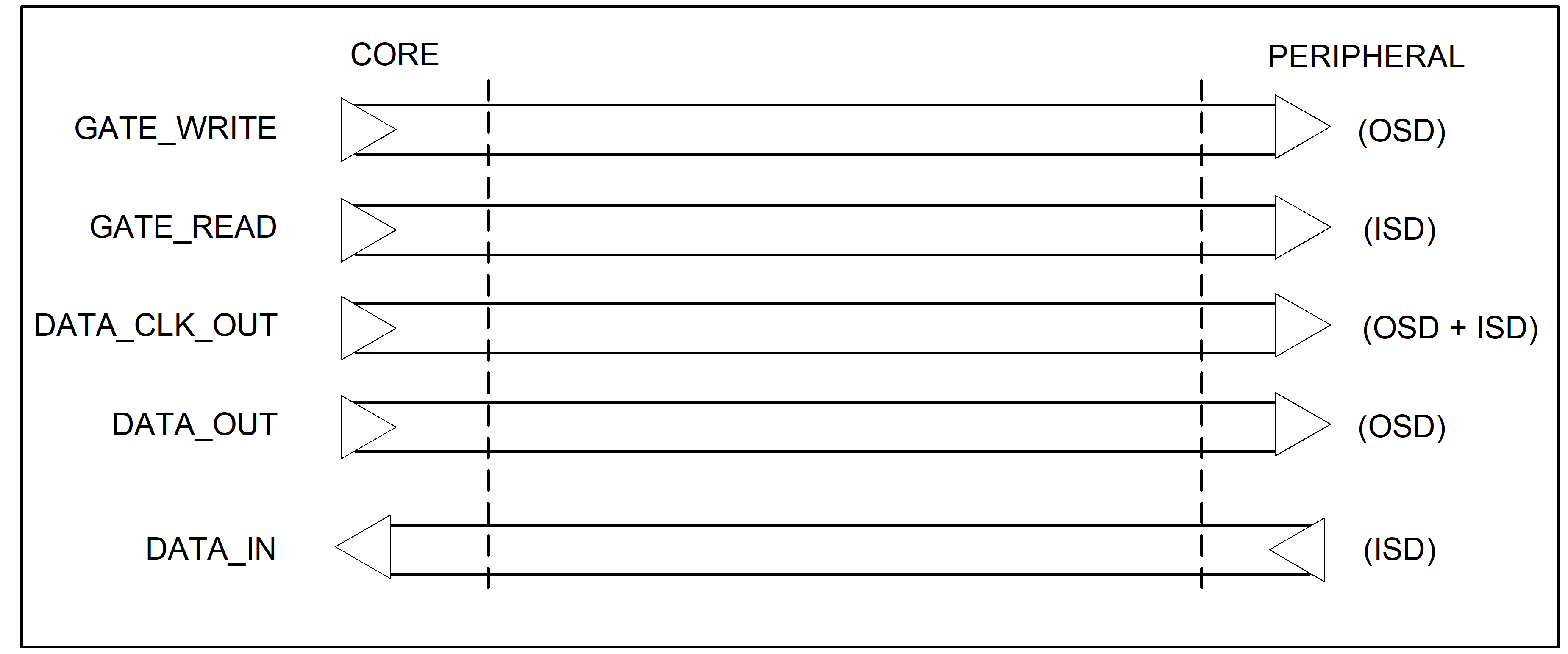 Figure 85: 16-bit bi-directional serial digital interface signal arrangement
There are two advantages offered by this interface.
Firstly, it offers the possibility of writing a data value out to a peripheral element and then reading the same value back in order to verify that the write operation was performed correctly.
Secondly, the interface can be expanded to address more than one register location within a peripheral element using only two extra signals for each additional register. The extra signals used are a dedicated GATE_WRITE(READ) signal for each new register to be accessed. All of the other signals can be common to all registers. This means that n registers can be accessed using only 2n + 3 signals which can lead to significant savings in terms of cables and connectors.
During an input transfer the data is input via the DATA_IN signal and the DATA_OUT signal assumes its quiescence state. During a data output transfer the data is output on the DATA_OUT signal and the DATA_IN signal assumes its quiescence state.
Serial digital interface electrical circuits description
The serial digital interface circuits are the conducting paths which convey the data and control signals which make up the interface between the core and peripheral elements. Each circuit consists of the conductors and any connectors or other components which comprise the electrical path.
Two circuits are used for each signal. These circuits operate in a balanced mode with reference to the core element differential ground potential, i.e. when one circuit carries a positive voltage, the complementary circuit carries a negative voltage of the same magnitude.
Figure 86 shows the relationship between circuits, signals, and the interface definition point for balanced differential serial digital interfaces.
 Figure 86: Balanced differential circuits for serial digital interfaces
Balanced differential serial digital interface signals
Balanced differential serial digital interface - GATE_WRITE circuits
A balanced differential pair of circuits called GATE_WRITE+ and GATE_WRITE- shall be provided.
The balanced differential pair specified in 8.7.1a shall
- be driven by the core element, and
- carry the GATE_WRITE signal.
Balanced differential serial digital interface - DATA_CLK_OUT circuits
A balanced differential pair of circuits called DATA_CLK_OUT+ and DATA_CLK_OUT- shall be provided.
The balanced differential pair specified in 8.7.2a. shall
- be driven by the core element, and
- carry the DATA_CLK_OUT signal.
Balanced differential serial digital interface - DATA_OUT circuits
For output serial digital interfaces, a balanced differential pair of circuits called DATA_OUT+ and DATA_OUT- shall be provided.
The balanced differential pair specified in 8.7.3a shall
- be driven by the peripheral element, and
- carry the DATA_OUT signal.
Balanced differential serial digital interface - DATA_IN circuits
For input serial digital interfaces, a balanced differential pair of circuits called DATA_IN+ and DATA_IN- shall be provided.
The balanced differential pair specified in 8.7.4a shall
- be driven by the peripheral element, and
- carry the DATA_IN signal.
Balanced differential serial digital interface - GATE_READ circuits
For bi-directional serial digital interfaces, a balanced differential pair of circuits called GATE_READ+ and GATE_READ- shall be provided.
The balanced differential pair specified in 8.7.5a shall
- be driven by the core element, and
- carry the GATE_READ signal.
Serial digital interface circuit electrical characteristics
Introduction
ANSI/TIA/EIA-422 (hereafter briefly RS-422) defines a balanced (differential) interface; specifying a single, unidirectional driver with multiple receivers (up to 32). RS-422 will support Point-to-Point, Multi-Drop circuits, but .
Although the EIA standard does not show circuit grounding in either of the RS-422 circuits, this Standard includes recommendation on grounding in 8.8.2a.
Provisions
Serial digital interface circuits should be grounded as follows:
- The drivers and receivers should be connected directly to circuit ground.
- The circuit ground should be connected to chassis ground.
- 1 Cabling is not specified in RS-422 but information can be found in [V11].
- 2 Figure 87 illustrates this provision.
Serial digital interface circuit electrical characteristics shall meet the requirements specified in Table 84. - 1 Table 84 includes characteristics for compatibility with RS422 (indicated with the number (422) in the table), and specific characteristics
- 2 The values specified here-in grant correct operations in the following conditions:
- maximum signal frequency: 1 MHz;
- maximum cable length: 16 m;
- cable type: Twisted Shielded Pair 120 Ω Impedance.
- 3 Compliance to the parameters indicated by the note (422) in Table 84 can be achieved by use of the following circuits:
HS-26C(T)31RHHS-26C(T)32RHHS-26CLV31RHHS-26CLV32RHItems 1 and 2 are 5 V supplied devices, items 3 and 4 are 3,3 V supplied devices. These devices can interoperate and comply with the specification in Table 84.
Serial digital interface shall be compliant to the interface arrangement specified in Figure 87.
Compliance to microcircuits characteristics others than the parameters indicated by the note (422) in Table 84., shall be verified on the project by Review of Design or Test.
 Figure 87: Example of serial digital interface arrangement
Table 84: Serial digital interface electrical characteristics
|
Reference
|
Characteristics
|
Value
|
Type
|
Notes
|
|
SOURCE CIRCUIT
| ||||
|
8.8 a.1
|
Electrical characteristics
|
Differential
|
(422)
|
|
|
8.8 a.2
|
Differential output voltage open circuit, VOC
|
1,8 V ≤ |VOC| ≤ 6,0 V
|
Specific
|
|
|
8.8 a.3
|
Output voltage TRUE and COMP lines, Ve
|
Ve ≤ 6 V
|
(422)
|
|
|
8.8 a.4
|
Differential output impedance, Zout
|
105 ≤ Zout ≤ 135
|
Specific
|
Note 1
|
|
8.8 a.5
|
Short circuit output current, IA
|
|IA| ≤ 150 mA for each terminalto ground
|
(422)
|
|
|
8.8 a.6
|
Rise time, tr
|
tr ≤ 0,1 tb if tb ≥ 200 nstr ≤ 20 ns if tb ≤ 200 ns
|
(422)
|
Note 2
|
|
8.8 a.7
|
Output leakage current in power off, IO
|
|IO| ≤ 100 µA
|
(422)
|
Note 3
|
|
8.8 a.8
|
Fault voltage emission, Vsfe
|
0 V to 7 V (through 50 Ω minimum series resistance)
|
Specific
|
|
|
8.8 a.9
|
Fault voltage tolerance, Vsft
|
-1,5 V to 7 V (applied through 1 kΩ series resistance Ris)
|
Specific
|
|
|
RECEIVER CIRCUIT
| ||||
|
8.8 a.10
|
Electrical characteristics
|
Differential
|
(422)
|
|
|
8.8 a.11
|
Series protection, Ris
|
2 * 1 kΩ
|
Specific
|
|
|
8.8 a.12
|
Max input voltage (each input w.r.t. ground), VI
|
± 10 V
|
(422)
|
Note 4
|
|
8.8 a.13
|
Common mode acceptance (V1+V2)/2, VCM
|
– 4 V to + 7 V
|
Specific
|
Note 5
|
|
8.8 a.14
|
Differential input voltage, VDI
|
± |600 mV to 6 V|each voltage in this range must beinterpreted as valid signal
|
Specific
|
Note 6
|
|
8.8 a.15
|
Fault voltage emission, Vrfe
|
0 V to 5,5 V (through 1 kΩ series resistance Ris)
|
Specific
|
|
|
8.8 a.16
|
Fault voltage tolerance, Vrft
|
-1,5 V to 8,5 V
|
Specific
|
|
|
Note 1: Output impedance to be matched with 120 Ω cable impedance. Recommended range of the Ros resistors between 50 Ω and 60 Ω, considering 10 Ω typical driver output impedance, when using HS-26C(T)31RH.
| ||||
 Figure 88: Threshold levels for ECSS-E-50-14 differential circuits
ANNEX(informative)Tailoring guidelines
Tailoring for this Standard is limited to the adoption of specific discrete interfaces listed hereby:
Analogue signal interfaces
Analogue signal monitor (ASM) interface
Temperature sensors monitor (TSM) interfaces
Bi-level discrete input interfaces
Bi-level discrete monitor (BDM) interface
Bi-level switch monitor (BSM) interface
Pulsed command interfaces
High power command (HPC) interfaces
Low power command (LPC) interface
Serial digital interfaces
16-bit input serial digital (ISD) interface
16-bit output serial digital (OSD) interface description
16-bit bi-directional serial digital (BSD) interface description
Modification of existing or addition of requirements within a specific interface definition should not be done.
Bibliography
|
ECSS-S-ST-00
|
ECSS system - Description, implementation and general requirements
|